1
LTC1655
16-Bit Rail-to-Rail
Micropower DAC in
SO-8 Package
s
16-Bit Monotonicity Over Temperature
s
Deglitched Rail-to-Rail Voltage Output
s
SO-8 Package
s
5V Single Supply Operation
s
I
CC(TYP)
: 600
µ
A
s
Internal Reference
s
Maximum DNL Error: 1LSB
s
Power-On Reset
s
3-Wire Cascadable Serial Interface
s
Low Cost
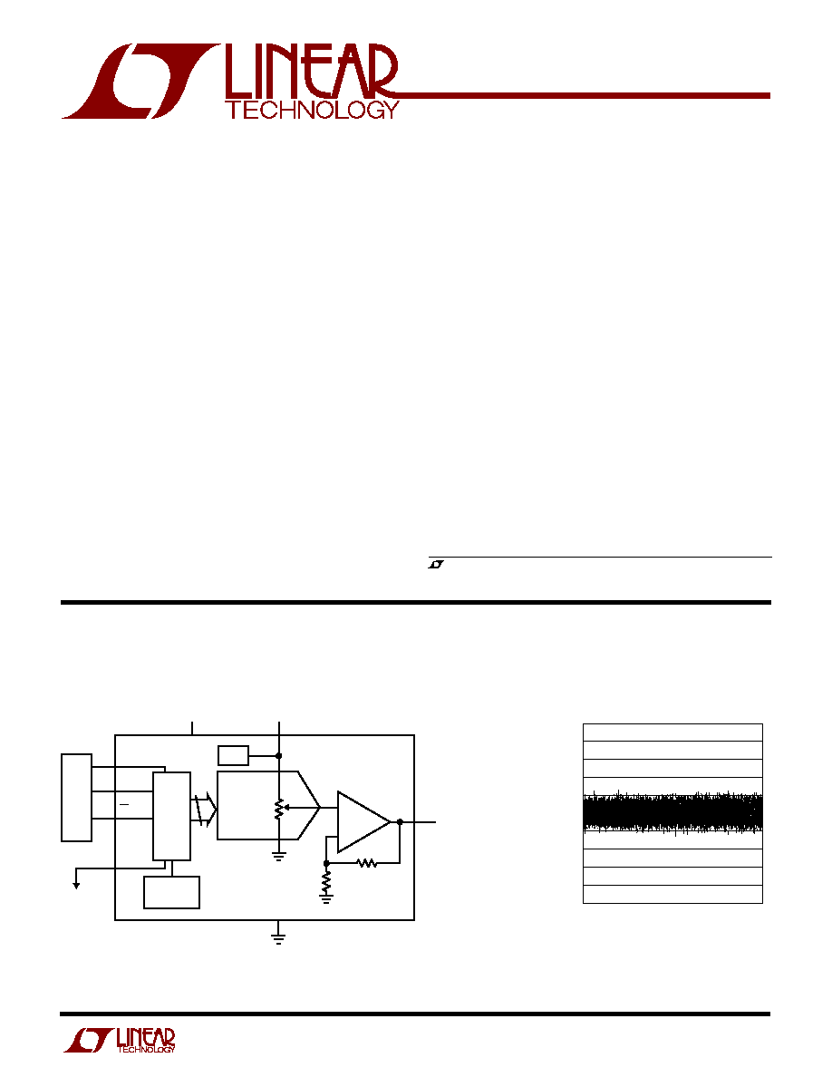
The LTC
Æ
1655 is a rail-to-rail voltage output, 16-bit digi-
tal-to-analog converter (DAC) in an SO-8 package. It
includes an output buffer and a reference. The 3-wire serial
interface is compatible with SPI/QSPI and MICROWIRE
TM
protocols. The CLK input has a Schmitt trigger that allows
direct optocoupler interface.
The LTC1655 has an onboard 2.048V reference that can be
overdriven to a higher voltage. The output swings from 0V
to 4.096V when using the internal reference. The typical
power dissipation is 3.0mW on a single 5V supply.
The LTC1655 is pin compatible with Linear Technology's
12-bit V
OUT
DAC family, allowing an easy upgrade path.
It is the only buffered 16-bit DAC in an SO-8 package and
it includes an onboard reference for stand alone
performance.
s
Digital Calibration
s
Industrial Process Control
s
Automatic Test Equipment
s
Cellular Telephones
, LTC and LT are registered trademarks of Linear Technology Corporation.
MICROWIRE is a trademark of National Semiconductor Corporation.
≠
+
16-BIT
DAC
4.5V TO 5.5V
2.048V
GND
POWER-ON
RESET
TO
OTHER
DACS
16-BIT
SHIFT
REG
AND
DAC
LATCH
µ
P
D
IN
V
CC
16
REF
2
8
6
D
OUT
4
5
1655 TA01
CLK
1
CS/LD
3
7
RAIL-TO-RAIL
VOLTAGE
OUTPUT
(0V TO 4.096V)
V
OUT
REF
Functional Block Diagram: 16-Bit Rail-to-Rail DAC
Differential Nonlinearity
vs Input Code
CODE
0
≠ 1.0
≠ 0.2
≠ 0.4
≠ 0.6
≠ 0.8
0
0.2
0.4
0.6
0.8
1.0
DNL ERROR (LSB)
16384
32768
1655 TA02
49152
65535
FEATURES
DESCRIPTIO
U
APPLICATIO S
U
TYPICAL APPLICATIO
U

2
LTC1655
ABSOLUTE
M
AXI
M
U
M
RATINGS
W
W
W
U
ORDER PART
NUMBER
W
U
U
PACKAGE/ORDER I FOR ATIO
LTC1655CN8
LTC1655IN8
LTC1655CS8
LTC1655IS8
S8 PART MARKING
1655
1655I
Consult factory for Military grade parts.
SYMBOL
PARAMETER
CONDITIONS
MIN
TYP
MAX
UNITS
DAC
Resolution
q
16
Bits
Monotonicity
q
16
Bits
DNL
Differential Nonlinearity
Guaranteed Monotonic (Note 2)
q
±
0.3
±
1.0
LSB
INL
Integral Nonlinearity
REF = 2.2V (External) (Note 2)
q
±
8
±
20
LSB
ZSE
Zero Scale Error
q
0
3
mV
V
OS
Offset Error
Measured at Code 200, REF = 2.2V (External)
q
±
0.5
±
3
mV
V
OS
TC
Offset Error Tempco
±
5
µ
V/
∞
C
Gain Error
REF = 2.2V (External)
q
±
5
±
16
LSB
Gain Error Drift
0.5
ppm/
∞
C
Power Supply
V
CC
Positive Supply Voltage
For Specified Performance
q
4.5
5.5
V
I
CC
Supply Current
4.5V
V
CC
5.5V (Note 4)
q
600
1200
µ
A
Op Amp DC Performance
Short-Circuit Current Low
V
OUT
Shorted to GND
q
70
120
mA
Short-Circuit Current High
V
OUT
Shorted to V
CC
q
80
140
mA
Output Impedance to GND
Input Code = 0
q
40
120
Output Line Regulation
Input Code = 65535, V
CC
= 4.5V to 5.5V,
q
±
3
mV/V
with Internal Reference
AC Performance
Voltage Output Slew Rate
(Note 3)
q
±
0.3
±
0.7
V/
µ
s
Voltage Output Settling Time
(Note 3) to 0.0015% (16-Bit Settling Time)
20
µ
s
(Note 3) to 0.012% (13-Bit Settling Time)
10
µ
s
Digital Feedthrough
0.3
nV -s
Midscale Glitch Impulse
DAC Switch Between 8000 and 7FFF
12
nV-s
(Note 1)
V
CC
to GND .............................................. ≠ 0.5V to 7.5V
TTL Input Voltage .................................... ≠ 0.5V to 7.5V
V
OUT
, REF
....................................... ≠ 0.5V to V
CC
+ 0.5V
Maximum Junction Temperature ......................... 125
∞
C
Operating Temperature Range
LTC1655C .............................................. 0
∞
C to 70
∞
C
LTC1655I ........................................... ≠ 40
∞
C to 85
∞
C
Storage Temperature Range ................ ≠ 65
∞
C to 150
∞
C
Lead Temperature (Soldering, 10 sec)................. 300
∞
C
1
2
3
4
8
7
6
5
TOP VIEW
V
CC
V
OUT
REF
GND
CLK
D
IN
CS/LD
D
OUT
S8 PACKAGE
8-LEAD PLASTIC SO
N8 PACKAGE
8-LEAD PDIP
T
JMAX
= 125
∞
C,
JA
= 100
∞
C/W (N8)
T
JMAX
= 125
∞
C,
JA
= 150
∞
C/W (S8)
The
q
denotes specifications which apply over the full operating temperature range, otherwise specifications are T
A
= 25
∞
C.
V
CC
= 4.5V to 5.5V, V
OUT
unloaded, REF unloaded, T
A
= T
MIN
to T
MAX
, unless otherwise noted.
ELECTRICAL CHARACTERISTICS
3
LTC1655
ELECTRICAL CHARACTERISTICS
SYMBOL
PARAMETER
CONDITIONS
MIN
TYP
MAX
UNITS
Digital I/O
V
IH
Digital Input High Voltage
q
2.4
V
V
IL
Digital Input Low Voltage
q
0.8
V
V
OH
Digital Output High Voltage
I
OUT
= ≠ 1mA, D
OUT
Only
q
V
CC
≠ 1
V
V
OL
Digital Output Low Voltage
I
OUT
= 1mA, D
OUT
Only
q
0.4
V
I
LEAK
Digital Input Leakage
V
IN
= GND to V
CC
q
±
10
µ
A
C
IN
Digital Input Capacitance
(Note 6)
10
pF
Switching
t
1
D
IN
Valid to CLK Setup
V
CC
= 5V
q
40
ns
t
2
D
IN
Valid to CLK Hold
V
CC
= 5V
q
0
ns
t
3
CLK High Time
V
CC
= 5V (Note 6)
q
40
ns
t
4
CLK Low Time
V
CC
= 5V (Note 6)
q
40
ns
t
5
CS/LD Pulse Width
V
CC
= 5V (Note 6)
q
50
ns
t
6
LSB CLK to CS/LD
V
CC
= 5V (Note 6)
q
40
ns
t
7
CS/LD Low to CLK
V
CC
= 5V (Note 6)
q
20
ns
t
8
D
OUT
Output Delay
V
CC
= 5V, C
LOAD
= 15pF
q
0
120
ns
t
9
CLK Low to CS/LD Low
V
CC
= 5V (Note 6)
q
20
ns
Reference Output
Reference Output Voltage
q
2.036
2.048
2.060
V
Reference Input Range
(Notes 5, 6)
2.2
V
CC
/2
V
Reference Output Tempco
5
ppm/
∞
C
Reference Input Resistance
REF Overdriven to 2.2V
q
8.5
13
k
Reference Short-Circuit Current
q
40
100
mA
Reference Output Line Regulation
V
CC
= 4.5V to 5.5V
q
±
1.5
mV/V
Reference Load Regulation
I
OUT
= 100
µ
A
q
0.5
mV
Note 1: Absolute Maximum Ratings are those values beyond which the life
of a device may be impaired.
Note 2: Nonlinearity is defined from code 128 to code 65535 (full scale).
See Applications Information.
Note 3: DAC switched between all 1s and code 400.
Note 4: Digital inputs at 0V or V
CC
.
Note 5: Reference can be overdriven (see Applications Information).
Note 6: Guaranteed by design. Not subject to test.
The
q
denotes specifications which apply over the full operating temperature range, otherwise specifications are T
A
= 25
∞
C.
V
CC
= 4.5V to 5.5V, V
OUT
unloaded, REF unloaded, T
A
= T
MIN
to T
MAX
, unless otherwise noted.
4
LTC1655
TYPICAL PERFOR
M
A
N
CE CHARACTERISTICS
U
W
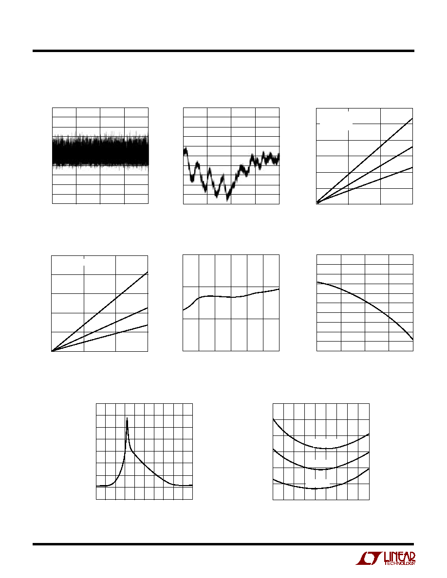
DIGITAL INPUT CODE
0
DIFFERENTIAL NONLINEARITY (LSB)
65,535
1655 G01
16,384
32,768
49,152
1.0
0.8
0.6
0.4
0.2
0
≠0.2
≠0.4
≠0.6
≠0.8
≠1.0
Differential Nonlinearity
LOAD CURRENT (mA)
0
V
CC
≠ V
OUT
(V)
1.2
1.0
0.8
0.6
0.4
0.2
0
1655 F03
5
10
15
125
∞
C
25
∞
C
≠55
∞
C
V
OUT
< 1LSB
V
OUT
= 4.096V
CODE: ALL 1's
DIGITAL INPUT CODE
0
INTEGRAL NONLINEARITY (LSB)
65,535
1655 G02
16,384
32,768
49,152
5
4
3
2
1
0
≠1
≠2
≠3
≠4
≠5
Integral Nonlinearity
Minimum Supply Headroom for
Full Output Swing vs Load Current
OUTPUT SINK CURRENT (mA)
0
OUTPUT PULL-DOWN VOLTAGE (V)
1.0
0.8
0.6
0.4
0.2
0
1655 F04
5
10
15
125
∞
C
25
∞
C
≠55
∞
C
CODE: ALL 0's
TEMPERATURE (
∞
C)
≠55
OFFSET (mV)
125
1655 G06
≠10
35
80
1.0
0.8
0.6
0.4
0.2
0
≠0.2
≠0.4
≠0.6
≠0.8
≠1.0
Minimum Output Voltage vs
Output Sink Current
Full-Scale Voltage vs
Temperature
TEMPERATURE (
∞
C)
≠55
FULL-SCALE VOLTAGE (V)
4.10
4.09
4.08
4.07
≠25
5
35
65
1655 G05
95
125
Offset vs Temperature
TEMPERATURE (
∞
C)
≠55
SUPPLY CURRENT
(
µ
A)
≠15
25
45
125
1655 G08
≠35
5
65
85 105
700
680
660
640
620
600
580
V
CC
= 5.5V
V
CC
= 5V
V
CC
= 4.5V
Supply Current vs Temperature
LOGIC INPUT VOLTAGE (V)
0
SUPPLY CURRENT (mA)
3.4
3.0
2.6
2.2
1.8
1.4
1.0
0.6
0.2
4
1655 G07
1
2
3
5
Supply Current vs
Logic Input Voltage

5
LTC1655
PI
N
FU
N
CTIO
N
S
U
U
U
CLK (Pin 1): The TTL Level Input for the Serial Interface
Clock.
D
IN
(Pin 2): The TTL Level Input for the Serial Interface
Data. Data on the D
IN
pin is latched into the shift register
on the rising edge of the serial clock and is loaded MSB
first. The LTC1655 requires a 16-bit word.
CS/LD (Pin 3): The TTL Level Input for the Serial Inter-
face Enable and Load Control. When CS/LD is low the
CLK signal is enabled, so the data can be clocked in.
When CS/LD is pulled high, data is loaded from the shift
register into the DAC register, updating the DAC output.
D
OUT
(Pin 4): Output of the Shift Register. Becomes valid
on the rising edge of the serial clock and swings from GND
to V
CC
.
GND (Pin 5): Ground.
REF (Pin 6): Reference. Output of the internal reference is
2.048V. There is a gain of two from this pin to the output.
The reference can be overdriven from 2.2V to V
CC
/2. When
tied to V
CC
/2, the output will swing from GND to V
CC
. The
output can only swing to within its offset specification of
V
CC
(see Applications Information).
V
OUT
(Pin 7): Deglitched Rail-to-Rail Voltage Output. V
OUT
clears to 0V on power-up.
V
CC
(Pin 8): Positive Supply Input. 4.5V
V
CC
5.5V.
Requires a bypass capacitor to ground.
TI I G DIAGRA
W U
W
D15
MSB
D14
D13
D1
t
1
t
6
D0
LSB
t
2
t
4
t
3
t
8
CLK
D
IN
D
OUT
CS/LD
t
5
1655 TD
D15
PREVIOUS WORD
D14
PREVIOUS WORD
D0
PREVIOUS WORD
D15
CURRENT WORD
D13
PREVIOUS WORD
t
9
t
7
1
2
3
15
16

6
LTC1655
DEFI ITIO S
U
U
Differential Nonlinearity (DNL): The difference between
the measured change and the ideal 1LSB change for any
two adjacent codes. The DNL error between any two codes
is calculated as follows:
DNL = (
V
OUT
≠ LSB)/LSB
Where
V
OUT
is the measured voltage difference between
two adjacent codes.
Digital Feedthrough: The glitch that appears at the analog
output caused by AC coupling from the digital inputs when
they change state. The area of the glitch is specified in
(nV)(sec).
Full-Scale Error (FSE): The deviation of the actual full-
scale voltage from ideal. FSE includes the effects of offset
and gain errors (see Applications Information).
Gain Error (GE): The difference between the full-scale
output of a DAC from its ideal full-scale value after offset
error has been adjusted.
Integral Nonlinearity (INL): The deviation from a straight
line passing through the endpoints of the DAC transfer
curve (Endpoint INL). Because the output cannot go below
zero, the linearity is measured between full scale and the
lowest code that guarantees the output will be greater than
zero. The INL error at a given input code is calculated as
follows:
INL = [V
OUT
≠ V
OS
≠ (V
FS
≠ V
OS
)(code/65535)]/LSB
Where V
OUT
is the output voltage of the DAC measured at
the given input code.
Least Significant Bit (LSB): The ideal voltage difference
between two successive codes.
LSB = 2V
REF
/65536
Resolution (n): Defines the number of DAC output states
(2
n
) that divide the full-scale range. Resolution does not
imply linearity.
Voltage Offset Error (V
OS
): Nominally, the voltage at the
output when the DAC is loaded with all zeros. A single
supply DAC can have a true negative offset, but the output
cannot go below zero (see Applications Information).
For this reason, single supply DAC offset is measured at
the lowest code that guarantees the output will be greater
than zero.
OPERATIO
U
Serial Interface
The data on the D
IN
input is loaded into the shift register
on the rising edge of the clock. The MSB is loaded first. The
DAC register loads the data from the shift register when
CS/LD is pulled high. The clock is disabled internally when
CS/LD is high. Note: CLK must be low before CS/LD is
pulled low to avoid an extra internal clock pulse. The input
word must be 16 bits wide.
The buffered output of the 16-bit shift register is available
on the D
OUT
pin which swings from GND to V
CC
.
Multiple LTC1655s may be daisy-chained together by
connecting the D
OUT
pin to the D
IN
pin of the next chip
while the clock and CS/LD signals remain common to all
chips in the daisy chain. The serial data is clocked to all of
the chips, then the CS/LD signal is pulled high to update all
of them simultaneously. The shift register and DAC regis-
ter are cleared to all 0s on power-up.
Voltage Output
The LTC1655 rail-to-rail buffered output can source or sink
5mA over the entire operating temperature range while
pulling to within 400mV of the positive supply voltage or
ground. The output stage is equipped with a deglitcher that
gives a midscale glitch of 12nV-s. At power-up, output stage
clears to 0V.
The output swings to within a few millivolts of either sup-
ply rail when unloaded and has an equivalent output resis-
tance of 40
when driving a load to the rails. The output
can drive 1000pF without going into oscillation.
7
LTC1655
APPLICATIO
N
S I
N
FOR
M
ATIO
N
W
U
U
U
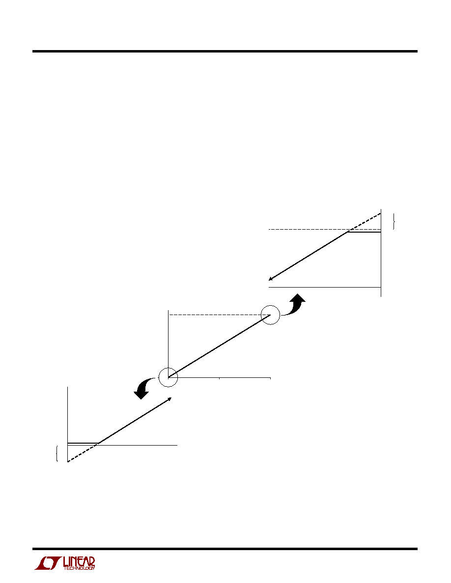
Rail-to-Rail Output Considerations
In any rail-to-rail DAC, the output swing is limited to
voltages within the supply range.
If the DAC offset is negative, the output for the lowest
codes limits at 0V as shown in Figure 1b.
Similarly, limiting can occur near full scale when the REF
pin is tied to V
CC
/2. If V
REF
= V
CC
/2 and the DAC full-scale
error (FSE) is positive, the output for the highest codes
limits at V
CC
as shown in Figure 1c. No full-scale limiting
can occur if V
REF
is less than (V
CC
≠ FSE)/ 2.
Offset and linearity are defined and tested over the region
of the DAC transfer function where no output limiting can
occur.
Figure 1. Effects of Rail-to-Rail Operation On a DAC Transfer Curve. (a) Overall Transfer Function (b) Effect of Negative
Offset for Codes Near Zero Scale (c) Effect of Positive Full-Scale Error for Input Codes Near Full Scale When V
REF
= V
CC
/2
1655 F01
INPUT CODE
(b)
OUTPUT
VOLTAGE
NEGATIVE
OFFSET
0V
32768
0
65535
INPUT CODE
OUTPUT
VOLTAGE
(a)
V
REF
= V
CC
/2
V
CC
V
CC
V
REF
= V
CC
/2
(c)
INPUT CODE
OUTPUT
VOLTAGE
POSITIVE
FSE

8
LTC1655
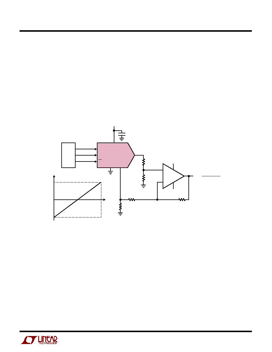
An Isolated 4mA to 20mA Process Controller
1655 TA03
3k
10k
1k
75k
1%
5k
150k
1%
20k
Q1
2N3440
R
S
10
V
LOOP
6V TO 30V
I
OUT
OUT
IN
CLK
D
IN
CS/LD
CLK
D
IN
CS/LD
CLK
D
IN
CS/LD
V
CC
V
OUT
1
µ
F
LTC1655
4N28
OPTOISOLATORS
5V
500
LT
Æ
1121-5
FROM
OPTOISOLATED
INPUTS
V
REF
≠
+
LT
Æ
1077
TYPICAL APPLICATIO
N
S
U
This circuit shows how to use an LTC1655 to make an
optoisolated digitally controlled 4mA to 20mA process
controller. The controller circuitry, including the
optoisolation, is powered by the loop voltage that can have
a wide range of 6V to 30V. The 2.048V reference output of
the LTC1655 is used for the 4mA offset current and V
OUT
is used for the digitally controlled 0mA to 16mA current.
R
S
is a sense resistor and the op amp modulates the
transistor Q1 to provide the 4mA to 20mA current through
this resistor. The potentiometers allow for offset and full-
scale adjustment. The control circuitry dissipates well
under the 4mA budget at zero scale.
9
LTC1655
A Wide Swing, Bipolar Output 16-Bit DAC
TYPICAL APPLICATIO
N
S
U
This circuit shows how to make a bipolar output 16-bit
DAC with a wide output swing using an LTC1655 and an
LT1077. R1 and R2 resistively divide down the LTC1655
output and an offset is summed in using the LTC1655
onboard 2.048V reference and R3 and R4. R5 ensures that
the onboard reference is always sourcing current and
never has to sink any current even when V
OUT
is at full
scale. The LT1077 output will have a wide bipolar output
swing of ≠ 4.096V to 4.096V as shown in the figure below.
With this output swing 1LSB = 125
µ
V.
CLK
D
IN
CS/LD
µ
P
0.1
µ
F
V
CC
V
OUT
GND
V
REF
R1
100k
1%
5V
LTC1655
1655 TA05
≠
+
LT1077
5V
≠ 5V
R2
200k
1%
R3
100k
1%
R5
100k
1%
R4
200k
1%
(2)(D
IN
)(4.096)
65536
V
OUT
:
D
IN
V
OUT
4.096
≠ 4.096
32768
0
65535
TRANSFER CURVE
≠ 4.096V
10
LTC1655
Dimensions in inches (millimeters) unless otherwise noted.
PACKAGE DESCRIPTIO
N
U
N8 Package
8-Lead PDIP (Narrow 0.300)
(LTC DWG # 05-08-1510)
N8 1197
0.100
±
0.010
(2.540
±
0.254)
0.065
(1.651)
TYP
0.045 ≠ 0.065
(1.143 ≠ 1.651)
0.130
±
0.005
(3.302
±
0.127)
0.020
(0.508)
MIN
0.018
±
0.003
(0.457
±
0.076)
0.125
(3.175)
MIN
1
2
3
4
8
7
6
5
0.255
±
0.015*
(6.477
±
0.381)
0.400*
(10.160)
MAX
0.009 ≠ 0.015
(0.229 ≠ 0.381)
0.300 ≠ 0.325
(7.620 ≠ 8.255)
0.325
+0.035
≠0.015
+0.889
≠0.381
8.255
(
)
*THESE DIMENSIONS DO NOT INCLUDE MOLD FLASH OR PROTRUSIONS.
MOLD FLASH OR PROTRUSIONS SHALL NOT EXCEED 0.010 INCH (0.254mm)
11
LTC1655
Dimensions in inches (millimeters) unless otherwise noted.
PACKAGE DESCRIPTIO
N
U
S8 Package
8-Lead Plastic Small Outline (Narrow 0.150)
(LTC DWG # 05-08-1610)
1
2
3
4
0.150 ≠ 0.157**
(3.810 ≠ 3.988)
8
7
6
5
0.189 ≠ 0.197*
(4.801 ≠ 5.004)
0.228 ≠ 0.244
(5.791 ≠ 6.197)
0.016 ≠ 0.050
0.406 ≠ 1.270
0.010 ≠ 0.020
(0.254 ≠ 0.508)
◊
45
∞
0
∞
≠ 8
∞
TYP
0.008 ≠ 0.010
(0.203 ≠ 0.254)
SO8 0996
0.053 ≠ 0.069
(1.346 ≠ 1.752)
0.014 ≠ 0.019
(0.355 ≠ 0.483)
0.004 ≠ 0.010
(0.101 ≠ 0.254)
0.050
(1.270)
TYP
DIMENSION DOES NOT INCLUDE MOLD FLASH. MOLD FLASH
SHALL NOT EXCEED 0.006" (0.152mm) PER SIDE
DIMENSION DOES NOT INCLUDE INTERLEAD FLASH. INTERLEAD
FLASH SHALL NOT EXCEED 0.010" (0.254mm) PER SIDE
*
**
Information furnished by Linear Technology Corporation is believed to be accurate and reliable.
However, no responsibility is assumed for its use. Linear Technology Corporation makes no represen-
tation that the interconnection of its circuits as described herein will not infringe on existing patent rights.
12
LTC1655
©
LINEAR TECHNOLOGY CORPORATION 1998
1655f LT/TP 0399 4K ∑ PRINTED IN USA
Linear Technology Corporation
1630 McCarthy Blvd., Milpitas, CA 95035-7417
(408) 432-1900
q
FAX: (408) 434-0507
q
www.linear-tech.com
PART NUMBER DESCRIPTION
COMMENTS
LTC1257
Single 12-Bit V
OUT
DAC, Full Scale: 2.048V, V
CC
: 4.75V to 15.75V,
5V to 15V Single Supply, Complete V
OUT
DAC in
Reference Can Be Overdriven Up to 12V, i.e., FS
MAX
= 12V
SO-8 Package
LTC1446/
Dual 12-Bit V
OUT
DACs in SO-8 Package
LTC1446: V
CC
= 4.5V to 5.5V, V
OUT
= 0V to 4.095V
LTC1446L
LTC1446L: V
CC
= 2.7V to 5.5V, V
OUT
= 0V to 2.5V
LTC1448
Dual 12-Bit V
OUT
DAC, V
CC
: 2.7V to 5.5V
Output Swings from GND to REF. REF Input Can Be Tied to V
CC
LTC1450/
Single 12-Bit V
OUT
DACs with Parallel Interface
LTC1450: V
CC
= 4.5V to 5.5V, V
OUT
= 0V to 4.095V
LTC1450L
LTC1450L: V
CC
= 2.7V to 5.5V, V
OUT
= 0V to 2.5V
LTC1451
Single Rail-to-Rail 12-Bit DAC, Full Scale: 4.095V, V
CC
: 4.5V to 5.5V,
5V, Low Power Complete V
OUT
DAC in SO-8 Package
Internal 2.048V Reference Brought Out to Pin
LTC1452
Single Rail-to-Rail 12-Bit V
OUT
Multiplying DAC, V
CC
: 2.7V to 5.5V
Low Power, Multiplying V
OUT
DAC with Rail-to-Rail
Buffer Amplifier in SO-8 Package
LTC1453
Single Rail-to-Rail 12-Bit V
OUT
DAC, Full Scale: 2.5V, V
CC
: 2.7V to 5.5V 3V, Low Power, Complete V
OUT
DAC in SO-8 Package
LTC1454/
Dual 12-Bit V
OUT
DACs in SO-16 Package with Added Functionality
LTC1454: V
CC
= 4.5V to 5.5V, V
OUT
= 0V to 4.095V
LTC1454L
LTC1454L: V
CC
= 2.7V to 5.5V, V
OUT
= 0V to 2.5V
LTC1456
Single Rail-to-Rail Output 12-Bit DAC with Clear Pin,
Low Power, Complete V
OUT
DAC in SO-8
Full Scale: 4.095V, V
CC
: 4.5V to 5.5V
Package with Clear Pin
LTC1458/
Quad 12 Bit Rail-to-Rail Output DACs with Added Functionality
LTC1458: V
CC
= 4.5V to 5.5V, V
OUT
= 0V to 4.095V
LTC1458L
LTC1458L: V
CC
= 2.7V to 5.5V, V
OUT
= 0V to 2.5V
LTC1650
Single 16-Bit V
OUT
Industrial DAC in 16-Pin SO, V
CC
=
±
5V
Low Power, Deglitched, 4-Quadrant Mulitplying V
OUT
DAC, Output Swing
±
4.5V
LTC1658
Single Rail-to-Rail 14-Bit V
OUT
DAC in 8-Pin MSOP,
Low Power, Multiplying V
OUT
DAC in MS8 Package. Output
V
CC
= 2.7V to 5.5V
Swings from GND to REF. REF Input Can Be Tied to V
CC
LTC1659
Single Rail-to-Rail 12-Bit V
OUT
DAC in 8-Pin MSOP,
Low Power, Multiplying V
OUT
DAC in MS8 Package. Output
V
CC
= 2.7V to 5.5V
Swings from GND to REF. REF Input Can Be Tied to V
CC
RELATED PARTS
TYPICAL APPLICATIO
N
U
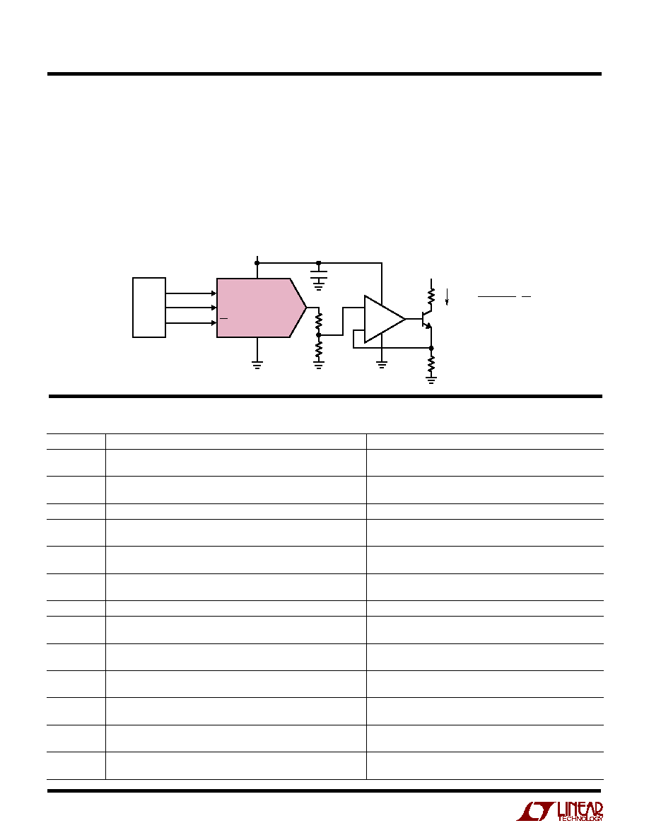
This circuit shows a digitally programmable current source
from an external voltage source using an external op amp,
an LT1077 and an NPN transistor (2N3440). Any digital
word from 0 to 65535 is loaded into the LTC1655 and its
output correspondingly swings from 0V to 4.096V. In the
configuration shown, R1, R2 resistively divide down the
LTC1655 output voltage. This divided voltage will be
forced across the resistor R
A
. If R
A
is chosen to be 205
,
the output current will range from 0mA at zero scale to
10mA at full scale. The minimum voltage for V
S
is deter-
mined by the load resistor R
L
and Q1's V
CESAT
voltage.
With a load resistor of 50
, the voltage source can be as
low as 3.3V.
Digitally Programmable Current Source
CLK
D
IN
CS/LD
0.1
µ
F
V
CC
V
OUT
GND
5V
LTC1655
µ
P
1655 TA04
≠
+
LT1077
V
S
+ 3.3V TO 100V
FOR R
L
50
Q1
2N3440
R
A
205
1%
R
L
I
OUT
= ∑
0mA TO 10mA
R1
100k
1%
R2
100k
1%
1
2
(D
IN
)(4.096)
(65536)(R
A
)