1699 Series Layout
LTC1699 Series
1
, LTC and LT are registered trademarks of Linear Technology Corporation.
s
Fully Compliant with Intel 5-Bit Mobile
(LTC1699-80) and Desktop VRM8.4 (LTC1699-81)
and VRM9.0 (LTC1699-82) VID Specifications
s
Precision
±
0.35% Programmable Resistor Divider
for Use with 0.8V Referenced DC/DC Converters
s
Two Different Divider Settings Can Be Stored Using a
2-Wire SMBus Serial Interface (Rev 1.1)
s
Built-In Safeguards Minimize Misprogramming Due
to Bus Conflicts
s
Three Open-Drain Pins (CPU_ON, IO_ON, CLK_ON)
and a Global Control Pin (VRON)to Shutdown or
Soft-Start 3 DC/DC Converters Simultaneously
s
PGOOD Pin and 50
µ
s PGOOD Timer
s
Available in MSOP-8 and SSOP-16 Package
AMD Athlon is a trademark of Advanced Micro Devices, Inc.
Pentium is a registered trademark of Intel Corporation.
Intel SpeedStep is a trademark of Intel Corporation.
The LTC
®
1699-80, LTC1699-81 and LTC1699-82 are pre-
cision (
±
0.35% max), digitally programmed resistor di-
viders that comply with Intel 5-bit mobile (LTC1699-80),
desktop VRM8.4 (LTC1699-81) and VRM9.0 (LTC1699-82)
VID specifications. Each IC can switch the output of a
DC/DC converter between two set voltages. A digital input
pin, SEL, selects one of two divider settings stored into
registers via a 2-wire SMBus interface.
The SMBus interface uses Write Word protocol to setup
the registers and to turn the DC/DC converters on or off.
Read Word protocol is used to verify register contents and
to return the On/Off status of the converters. The
LTC1699-80, LTC1699-81 and LTC1699-82 incorporate
safeguards against errors due to bus conflicts.
Three open-drain N-channel outputs (CPU_ON, IO_ON
and CLK_ON) are provided to turn DC/DC converter sup-
plies on or off via their RUN/SS inputs. A global control pin,
VRON
is used to turn the converters on or off simulta-
neously. An internal timer pulls the PGOOD pin low for
50
µ
s if the divider setting changes or the converters are
turned on via the SMBus and the VRON pin.
s
Intel Desktop Pentium
®
III Power Supply
s
Intel Mobile Pentium
®
Power Supply with Intel
SpeedStep
TM
Technology
s
Desktop AMD Athlon
TM
Power Supply
s
Software Programmable Remote Power Supply
s
Power Supplies with Voltage Margining
SMBus VID
Voltage Programmers
1
2
3
4
5
6
7
8
16
15
14
13
12
11
10
9
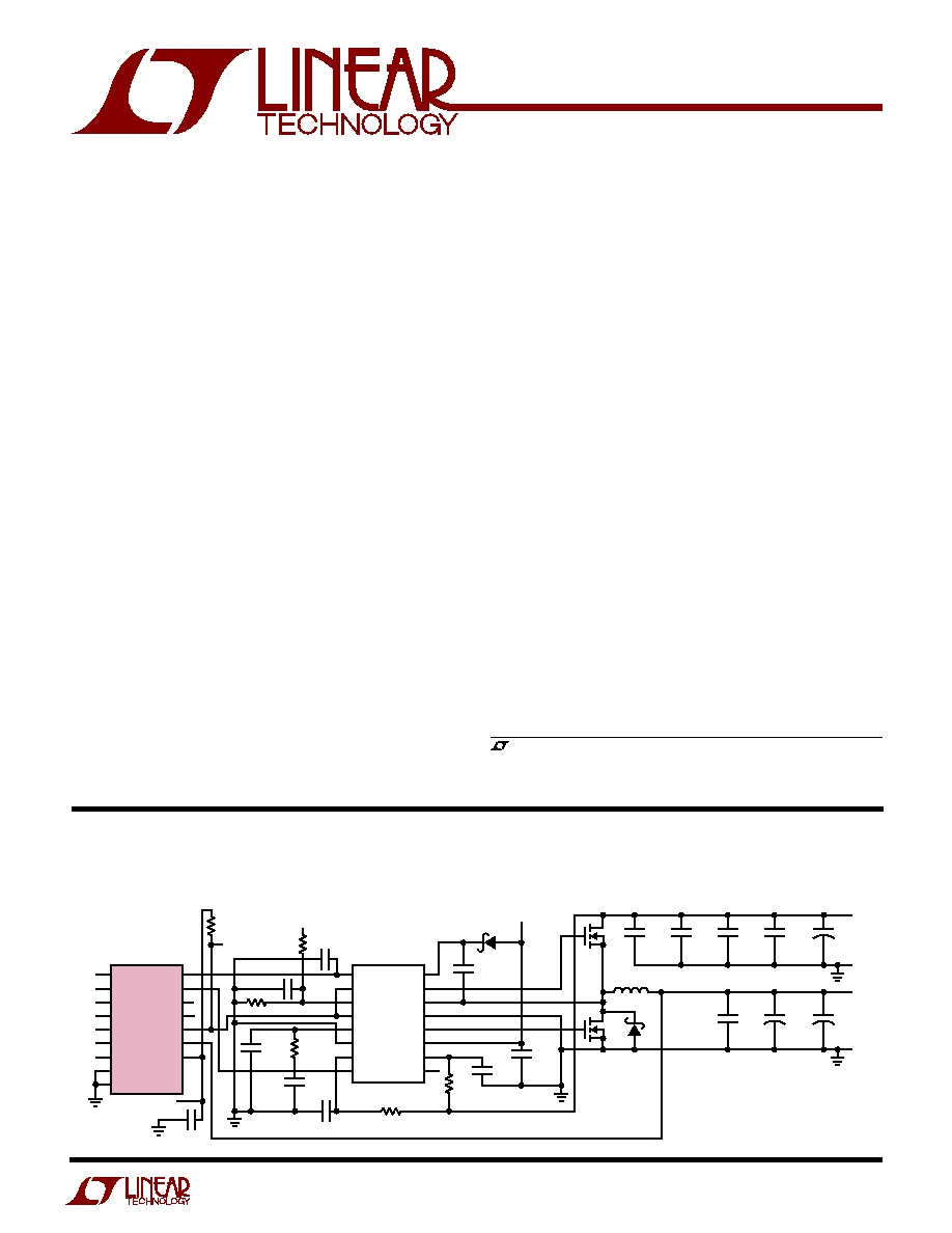
CPU_ON
IO_ON
CLK_ON
PGOOD
FB
VRON
SCL
SEL
SDA
VRON
SCL
SEL
SDA
SENSE
V
CC
U1
LTC1699-81
M1
M2
L1, 1
µ
H
C1
10
µ
F
25V
C1, C2, C3, C4, C9: TAIYO YUDAN
C5: SANYO
C10, C11: PANASONIC, SPCL. POLY.
D1: CMDSH-3
D2: DIODES INC., B340A
L1: TOKO, 919AS-1RON
M1: Si4884DY
M2: Si4874DY
C2
10
µ
F
25V
C3
10
µ
F
25V
C9
22
µ
F
6.3V
C4
10
µ
F
25V
C5
10
µ
F
35V
ALUM
D2
D1
V
IN
5VDC
5
3
4
1
NC
2
NC
7
NC
11
GND
14
GND
15
8
13
9
10
6
12
16
RUN/SS
PGOOD
V
RNG
FCB
I
TH
SGND
I
ON
V
FB
BOOST
TG
SW
PGND
BG
INTV
CC
V
IN
EXTV
CC
U2
LTC1778
1699 TA05
V
IN
5V
TO 20V
R4
10k
R3
1
R5
715k, 1%
R2, 11k
C7
0.22
µ
F
C15
220pF
C12
0.1
µ
F
C19, 0.01
µ
F
C6
0.01
µ
F
+
C11
180
µ
F
4V
GND
GND
5V
V
OUT
2.5V
AT 10A
+
C10
180
µ
F
4V
+
C18
2200pF
C14, 0.1
µ
F
C8, 0.01
µ
F
R1
39k
R9
100k
PGOOD
C13
4.7
µ
F
6.3V
SMBus Controlled High Efficiency DC/DC Converter
APPLICATIO S
U
FEATURES
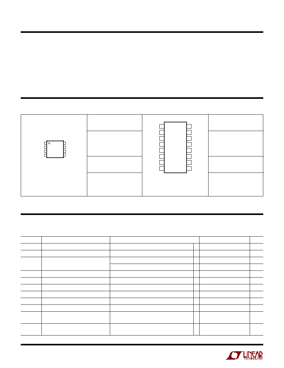
TYPICAL APPLICATIO
U
DESCRIPTIO
U
LTC1699 Series
2
ORDER PART
NUMBER
MS8 PART
MARKING
T
JMAX
= 125
°
C,
JA
= 200
°
C/W
Consult factory for parts specified with wider operating temperature ranges.
LTPV
LTPW
LTTB
LTC1699EMS8-80
LTC1699EMS8-81
LTC1699EMS8-82
ABSOLUTE AXI U
RATI GS
W
W
W
U
PACKAGE/ORDER I FOR ATIO
U
U
W
(Note 1)
ELECTRICAL CHARACTERISTICS
The
q
denotes the specifications which apply over the full operating
temperature range, otherwise specifications are at T
A
= 25
°
C. 2.7V
V
CC
5.5V (Notes 3, 4) unless otherwise stated.
SYMBOL
PARAMETER
CONDITIONS
MIN
TYP
MAX
UNITS
V
CC
Operating Supply Voltage Range
2.7
5.5
V
I
CC
Supply Current
CPU_ON, IO_ON, CLK_ON, PGOOD Pins Are Open
q
350
µ
A
R
FB-SENSE
Resistance between SENSE and FB
LTC1699-80, LTC1699-82
q
7
10
13
k
LTC1699-81
q
14
20
26
k
DE
Divider Error
All Divider Settings
q
0.35
0.35
%
V
IH
SCL, SDA Input High Voltage
q
2.1
V
V
IL
SCL, SDA Input Low Voltage
q
0.8
V
V
IH
SEL, VRON Input High Voltage
1.3
2.0
V
V
IL
SEL, VRON Input Low Voltage
q
0.8
1.3
V
V
HYST
SEL, VRON Hysteresis
±
50
mV
V
OL
SDA, CPU_ON, IO_ON, CLK_ON
I = 3mA
q
0.4
V
Output Low Voltage
I
IN
SCL, SDA, SEL, VRON Input Current
SDA Not Acknowledging, 0
V
PIN
5.5V,
V
PIN
= 5.5V for VRON only
q
±
10
µ
A
Supply Voltage (V
CC
) ................................................. 7V
All Pins ........................................................ 0.3V to 7V
Operating Temperature
Range (Note 2) ................................ 40
°
C
T
A
85
°
C
Junction Temperature ........................................... 125
°
C
Storage Temperature ...................... -65
°
C
T
A
150
°
C
Lead Temperature (Soldering, 10 sec).................. 300
°
C
ORDER PART
NUMBER
GN PART
MARKING
169980
169981
169982
LTC1699EGN-80
LTC1699EGN-81
LTC1699EGN-82
T
JMAX
= 125
°
C,
JA
= 130
°
C/W
1
2
3
4
5
6
7
8
TOP VIEW
GN PACKAGE
16-LEAD PLASTIC SSOP
16
15
14
13
12
11
10
9
SEL
NC
SDA
SCL
VRON
PGOOD
NC
CPU_ON
V
CC
GND
GND
FB
SENSE
NC
CLK_ON
IO_ON
1
2
3
4
SEL
SDA
SCL
PGOOD
8
7
6
5
V
CC
GND
FB
SENSE
TOP VIEW
MS8 PACKAGE
8-LEAD PLASTIC MSOP
LTC1699 Series
3
ELECTRICAL CHARACTERISTICS
The
q
denotes the specifications which apply over the full operating
temperature range, otherwise specifications are at T
A
= 25
°
C. 2.7V
V
CC
5.5V (Notes 3, 4) unless otherwise stated.
SYMBOL
PARAMETER
CONDITIONS
MIN
TYP
MAX
UNITS
I
SK1
SDA, PGOOD, CPU_ON, IO_ON,
0
V
PIN
2.7V
q
5
19
60
mA
CLK_ON Sink Current at V
CC
= 2.7V
I
SK2
SDA, PGOOD, CPU_ON, IO_ON,
0
V
PIN
5.5V
q
35
65
150
mA
CLK_ON Sink Current at V
CC
= 5.5V
I
LKG
PGOOD, CPU_ON, IO_ON,
0
V
PIN
5.5V
q
±
2
µ
A
CLK_ON Leakage Current
I
PU
VRON Pull-Up Current
V
PIN
= 0
q
1
2.5
7
µ
A
Timing (Note 5)
f
SMB
SMBus Operating Frequency
q
10
100
KHz
t
BUF
Bus Free Time Between Stop/Start
q
4.7
µ
s
t
HD:STA
Hold Time After (Repeated) Start
q
4.0
µ
s
t
SU:STA
Repeated Start Setup Time
q
4.7
µ
s
t
SU:STO
Stop Condition Setup Time
q
4.0
µ
s
t
HD:DAT
Data Hold Time
q
300
ns
t
SU:DAT
Data Setup Time
q
250
ns
t
LOW
Clock Low Period
q
4.7
µ
s
t
HIGH
Clock High Period
q
4.0
µ
s
t
f
SCL, SDA Fall Time
0.9V
CC
to 0.65V
q
300
ns
t
r
SCL, SDA Rise Time
0.65V to 2.25V
q
1000
ns
t
SSH
SEL to SENSE High (Note 6)
Toggle SEL to Switch from Min V
OUT
to Max V
OUT
,
500
ns
VFB = 0.8V
t
SSL
SEL to SENSE Low (Note 6)
Toggle SEL to Switch from Max V
OUT
to Min V
OUT
,
500
ns
VFB = 0.8V
t
SPL
SEL Toggling to PGOOD Low
Toggle SEL to Select New Code
q
160
500
ns
C
L
= 100pF, 10k
Pull-Up, S2 in Figure 1
t
PH
Stop Bit to CPU_ON, IO_ON
C
L
= 100pF, 10k
Pull-Up, S2 in Figure 1
q
2
µ
s
or CLK_ON High (Note 7)
t
PL
Stop Bit to CPU_ON, IO_ON
C
L
= 0.1
µ
F, 10k
Pull-Up, S1 in Figure 1
q
20
50
µ
s
or CLK_ON Low (Note 7)
t
PPL
Stop Bit to PGOOD Low (Note 6)
C
L
= 100pF, 10k
Pull-Up, S2 in Figure 1
q
250
ns
t
VH
VRON High to CPU_ON, IO_ON
C
L
= 100pF, 10k
Pull-Up, S2 in Figure 1
q
2
µ
s
or CLK_ON High
t
VL
VRON Low to CPU_ON, IO_ON,
C
L
= 0.1
µ
F, 10k
Pull-Up, S1 in Figure 1
q
50
µ
s
CLK_ON Low
t
VPL
VRON Low to PGOOD Low
C
L
= 100pF, 10k
Pull-Up, S2 in Figure 1
q
130
500
ns
t
PGL
PGOOD Low Duration
C
L
= 100pF, 10k
Pull-Up, S2 in Figure 1
q
30
50
70
µ
s
Note1: Absolute Maximum Ratings are those values beyond which the life
of a device may be impaired.
Note 2: The LTC1699-80E, LTC1699-81E and LTC1699-82E are
guaranteed to meet performance specifications from 0
°
C to 70
°
C.
Specifications over the 40
°
C to 85
°
C operating temperature range are
assured by design, characterization and correlation with statistical process
controls.
Note 3: All currents into device pins are positive; all currents out of device
pins are negative. All voltages are referenced to device ground unless
otherwise specified.
Note 4: All typical numbers are given for V
CC
= 5V and T
A
= 25
°
C.
Note 5: These parameters are guaranteed by design and are not tested in
production. SMBus timing is referenced to V
IL
and V
IH
levels.
Note 6: Dominated by the switching regulator. The delay due to the
LTC1699-80, LTC1699-81 or LTC1699-82 is typically 500ns.
Note 7: Measured from the rising edge of SDA during Data High
acknowledgement.
LTC1699 Series
4
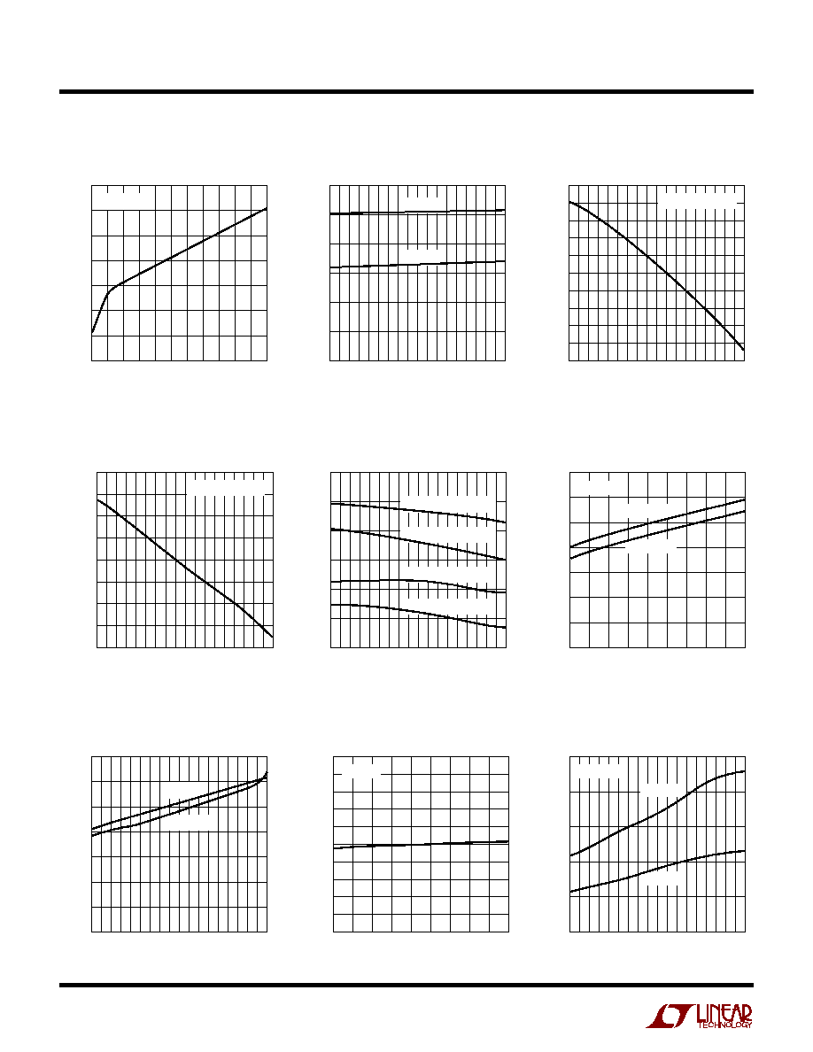
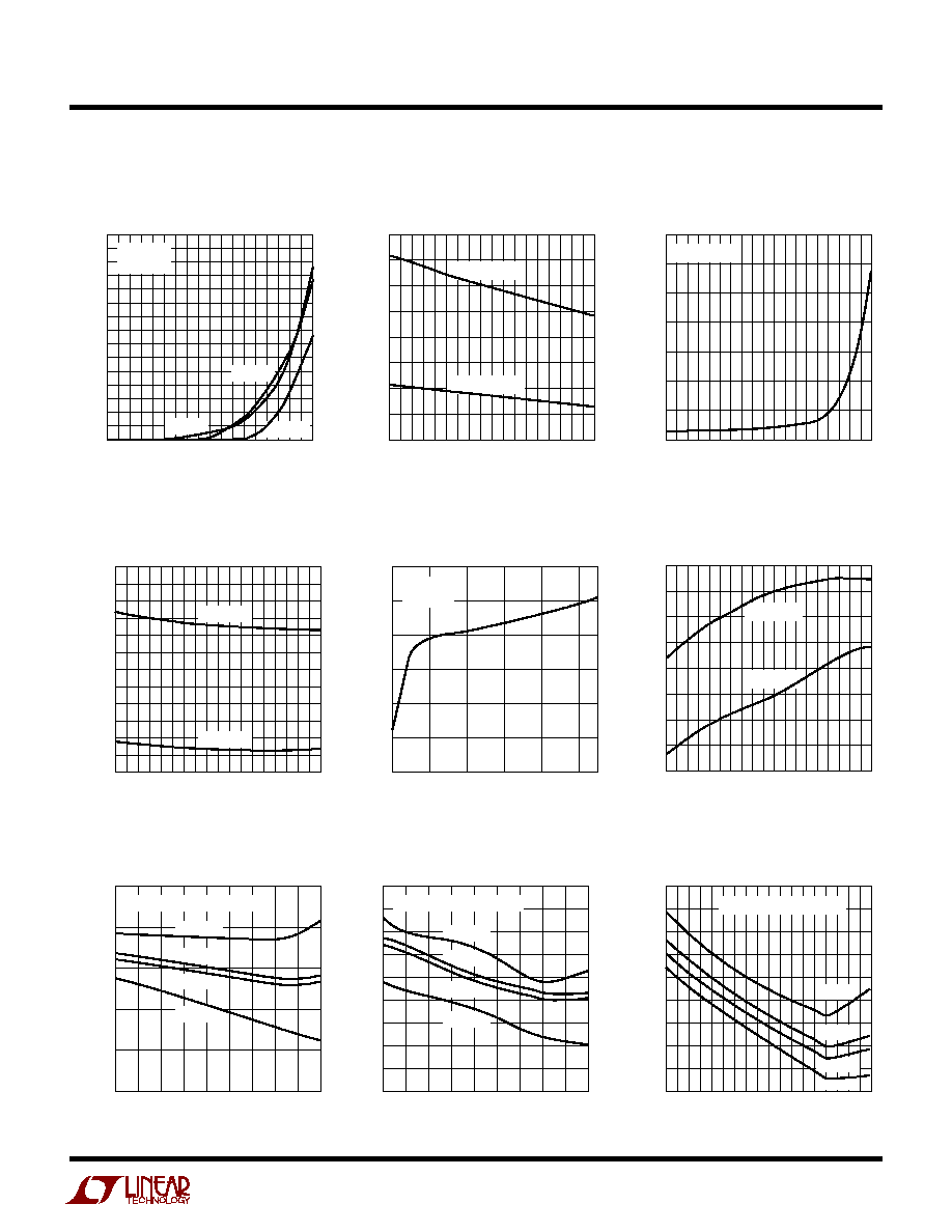
TYPICAL PERFOR A CE CHARACTERISTICS
U
W
Supply Current vs Supply Voltage
Supply Current vs Temperature
Resistance Between SENSE and FB
Pins vs Temperature (LTC1699-81)
SCL, SDA, SEL and VRON Input
High and Low Voltage vs
Temperature
SCL, SDA, SEL and VRON Input
High and Low Voltage vs Supply
Voltage
SCL, SDA, SEL and VRON
Hysteresis vs Temperature
SCL, SDA, SEL and VRON
Hysteresis vs Supply Voltage
SDA, CPU_ON, IO_ON, CLK_ON
Output Low Voltage vs
Temperature
V
CC
(V)
1.5
SUPPLY CURRENT (
µ
A)
1699 G01
350
300
250
200
150
100
50
0
2 2.5 3 3.5 4 4.5 5 5.5 6 6.5 7
T
A
= 25
°
C
TEMPERATURE (
°
C)
SUPPLY CURRENT (
µ
A)
1699 G02
300
250
200
150
100
50
0
55 35 15
5
25
45
65
85 105 125
V
CC
= 5.5V
V
CC
= 2.7V
TEMPERATURE (
°
C)
R
SENSE
(k
)
1699 G03
20.08
20.06
20.04
20.02
20.00
19.98
19.96
19.94
19.92
19.90
19.88
55 35 15
5
25
45
65
85 105 125
V
CC
= 2.7V TO 5.5V
TEMPERATURE (
°
C)
INPUT HIGH AND LOW VOLTAGE (V)
1699 G04
1.40
1.35
1.30
1.25
1.20
1.15
1.10
55 35 15
5
25
45
65
85 105 125
INPUT HIGH, V
CC
= 5.5V
INPUT LOW, V
CC
= 5.5V
INPUT HIGH, V
CC
= 2.7V
INPUT LOW, V
CC
= 2.7V
SUPPLY VOLTAGE (V)
INPUT HIGH AND LOW VOLTAGE (V)
1699 G05
1.5
1.4
1.3
1.2
1.1
1.0
0.9
0.8
2.5
3
3.5
4
4.5
5
5.5
6
6.5
7
INPUT HIGH
T
A
= 25
°
C
INPUT LOW
TEMPERATURE (
°
C)
HYSTERESIS (V)
1699 G06
0.07
0.06
0.05
0.04
0.03
0.02
0.01
0
55 35 15
5
25
45
65
85 105 125
V
CC
= 5.5V
V
CC
= 2.7V
SUPPLY VOLTAGE (V)
HYSTERESIS (V)
1699 G07
0.10
0.09
0.08
0.07
0.06
0.05
0.04
0.03
0.02
0.01
0
2.5
3
3.5
4
4.5
5
5.5
6
6.5
7
T = 25
°
C
TEMPERATURE (
°
C)
OUTPUT LOW VOLTAGE (V)
1699 G08
0.25
0.20
0.15
0.10
0.05
0
55 35 15
5
25
45
65
85 105 125
V
CC
= 2.7V
I
PIN
= 3mA
V
CC
= 5.5V
TEMPERATURE (
°
C)
R
SENSE
(k
)
1699 G18
10.08
10.06
10.04
10.02
10.00
9.98
9.96
9.94
9.92
55 35 15
5
25
45
65
85 105 125
V
CC
= 2.7V TO 5.5V
Resistance Between SENSE and
FB Pins vs Temperature
(LTC1699-80, LTC1699-82)
LTC1699 Series
5
TYPICAL PERFOR A CE CHARACTERISTICS
U
W
SCL, SDA and SEL Input Current
vs Temperature
TEMPERATURE (
°
C)
INPUT CURRENT (nA)
1699 G09
15
14
13
12
11
10
9
8
7
6
5
4
3
2
1
0
55 35 15
5
25
45
65
85 105 125
SCL PIN
SEL PIN
SDA PIN
V
CC
= 5.5V
V
PIN
= 5.5V
SDA, PGOOD, CPU_ON, IO_ON,
CLK_ON Sink Current vs
Temperature
PGOOD, CPU_ON, IO_ON,
CLK_ON Leakage Current vs
Temperature
VRON Pull-Up Current vs
Temperature
VRON Pull-Up Current vs Supply
Voltage
Power Good Low Duration vs
Temperature
LTC1699-80 Divider Error vs
Temperature
LTC1699-81 Divider Error vs
Temperature
LTC1699-82 Divider Error vs
Temperature
TEMPERATURE (
°
C)
SINK CURRENT (mA)
1699 G10
80
70
60
50
40
30
20
10
0
55 35 15
5
25
45
65
85 105 125
V
CC
= 5.5V, I
SK2
V
CC
= 2.7V, I
SK1
TEMPERATURE (
°
C)
LEAKAGE CURRENT (nA)
1699 G11
7
6
5
4
3
2
1
0
60 40 20
0
20
40
60
80 100 120
V
PIN
= 5.5V
TEMPERATURE (
°
C)
VRON PULL-UP CURRENT (
µ
A)
1699 G12
2.50
2.45
2.40
2.35
2.30
2.25
2.20
2.15
2.10
2.05
2.00
1.95
1.90
55 35 15
5
25
45
65
85 105 125
V
CC
= 5.5V
V
CC
= 2.7V
SUPPLY VOLTAGE (V)
1.5
VRON PULL-UP CURRENT
(
µ
A)
1699 G013
3.0
2.5
2.0
1.5
1.0
0.5
0
2.5
3.5
4.5
5.5
6.5
T
A
= 25
°
C
V
RON
= 0V
TEMPERATURE (
°
C)
DIVIDER ERROR (%)
1699 G15
0.05
0
0.05
0.10
0.15
0.20
55 35 15
5
25
45
65
85 105 125
V
CC
= 2.7V (MINIMUM V
CC
)
CODE 31
CODE 15
CODE 16
CODE 0
TEMPERATURE (
°
C)
DIVIDER ERROR (%)
1699 G16
0.25
0.20
0.15
0.10
0.05
0
0.05
0.10
0.15
0.20
55 35 15
5
25
45
65
85 105 125
V
CC
= 2.7V (MINIMUM V
CC
)
CODE 15
CODE 31
CODE 0
CODE 16
TEMPERATURE (
°
C)
POWER GOOD LOW DURATION (
µ
s)
1699 G14
52.0
51.5
51.0
50.5
50.0
49.5
49.0
60 40 20
0
20
40
60
80 100 120
V
CC
= 5.5V
V
CC
= 2.7V
TEMPERATURE (
°
C)
DIVIDER ERROR (%)
1699 G17
0.16
0.14
0.12
0.10
0.08
0.06
0.04
0.02
0
0.02
55 35 15
5
25
45
65
85 105 125
V
CC
= 2.7V (MINIMUM V
CC
)
CODE 31
CODE 15
CODE 16
CODE 0