 | ÐлекÑÑоннÑй компоненÑ: LTC1703 | СкаÑаÑÑ:  PDF PDF  ZIP ZIP |
Äîêóìåíòàöèÿ è îïèñàíèÿ www.docs.chipfind.ru
1
LTC1703
+
PV
CC
BOOST1
BG1
TG1
SW1
I
MAX1
FCB
RUN/SS1
COMP1
SGND
FB1
SENSE
VID0
VID1
I
MAX2
BOOST2
BG2
TG2
SW2
PGND
FAULT
RUN/SS2
COMP2
FB2
V
CC
VID4
VID3
VID2
1
2
3
4
5
6
7
8
9
10
11
12
13
14
28
27
26
25
24
23
22
21
20
19
18
17
16
15
LTC1703
DCP1
MBR0520LT1
DCP2
MBR0520LT1
QT2
QB2
QT1
C
SS1
0.22
µ
F
R21
100k
R12
10.2k
0.1%
R32
1k
C11
220pF
CCP2
1
µ
F
C21
15pF
R
IMAX2
20k
1
µ
F
C
SS2
0.22
µ
F
C32
2200pF
C22
15pF
C12
220pF
1
µ
F
C31
220pF
R31, 10k
R
IMAX1
,18.7k
RB2
11.5k
0.1%
R22, 100k
V
OUT1
0.9V
TO 2V
15A
GND
L1
1
µ
H
CCP1
1
µ
F
QB1B
QB1A
C
OUT1
180
µ
F
4V
×
6
C
IN
150
µ
F
10V
×
2
V
IN
4.5V TO 5.5V
V
OUT2
1.5V
3A
1703 TA01
VID0
VID1
VID2
VID3
VID4
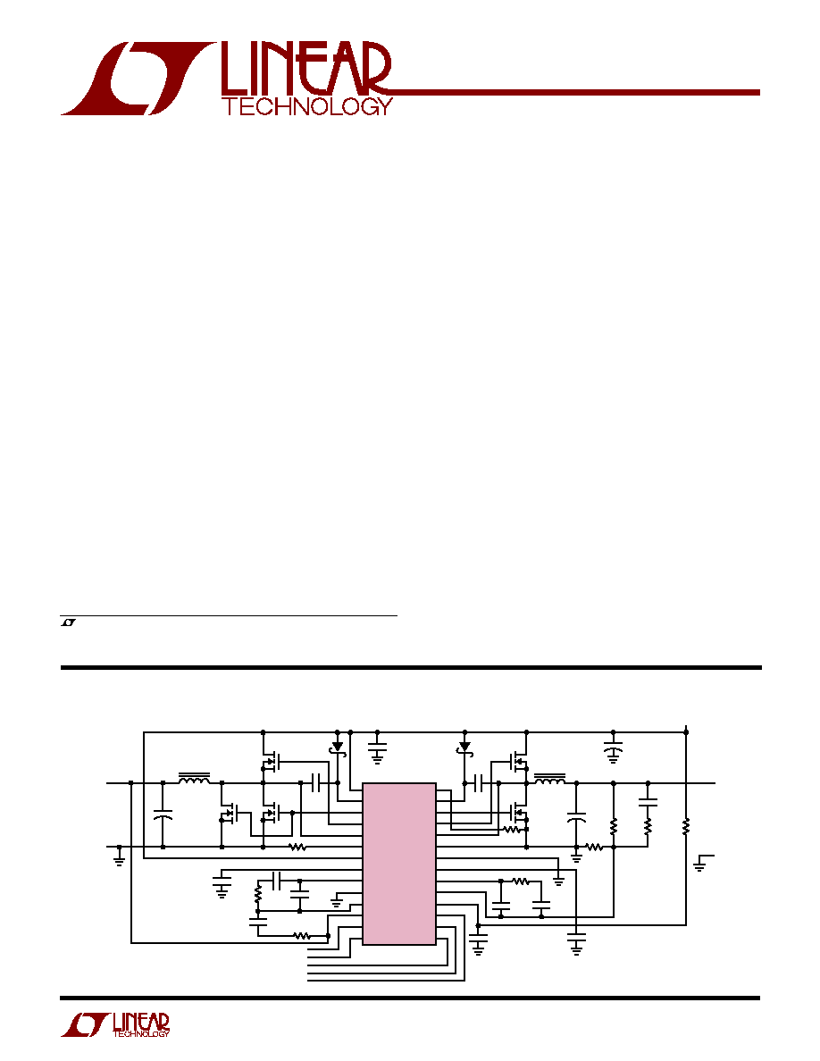
L1: MURATA LQT12535C1R5N12
L2: COILTRONICS UP2B-2R2
QT1, QB1A, QB1B: INTERNATIONAL RECTIFIER IRF7811
QT2, QB2: 1/2 FAIRCHILD NDS8926
L2
2.2
µ
H
+
C
OUT2
180
µ
F
4V
+
10
GND
GND
Dual 550kHz Synchronous
2-Phase Switching Regulator
Controller with 5-Bit VID
The LTC
®
1703 is a dual switching regulator controller opti-
mized for high efficiency with low input voltages. It includes
two complete, on-chip, independent switching regulator
controllers. Each is designed to drive a pair of external
N-channel MOSFET devices in a voltage mode feedback,
synchronous buck configuration. The LTC1703 includes
digital output voltage adjustment on side 1 that conforms to
the Intel Mobile VID specification. It uses a constant-
frequency, true PWM design switching at 550kHz, minimiz-
ing external component size and cost and optimizing load
transient performance. The synchronous buck architecture
automatically shifts to discontinuous and then to Burst
Mode
TM
operation as the output load decreases, ensuring
maximum efficiency over a wide range of load currents.
The LTC1703 features an onboard reference trimmed to 1%
and delivers better than 1.5% regulation at the converter
outputs. An optional latching FAULT mode protects the load
if the output rises 15% above the intended voltage. Each
channel can be enabled independently; with both channels
disabled, the LTC1703 shuts down and supply current drops
below 100
µ
A.
s
Two Independent PWM Controllers in One Package
s
Side 1 Output Is Compliant with Intel
Mobile
VID Specifications (Includes 5-Bit DAC)
s
0.9V to 2.0V Output Voltage with 25mV/50mV Steps
s
Two Sides Run Out-of-Phase to Minimize C
IN
s
All N-Channel External MOSFET Architecture
s
No External Current Sense Resistor
s
Precision Internal 0.8V
±
1% Reference
s
550kHz Switching Frequency Minimizes External
Component Size
s
Very Fast Transient Response
s
Up to 25A Output Current per Channel
s
Low Shutdown Current: < 100
µ
A
s
Small 28-Pin SSOP Package
, LTC and LT are registered trademarks of Linear Technology Corporation.
Burst Mode is a trademark of Linear Technology Corporation. Pentium is a registered trademark
of Intel Corporation.
s
Mobile Pentium
®
III Processor Systems
s
Microprocessor Core and I/O Supplies
s
Multiple Logic Supply Generator
s
High Efficiency Power Conversion
Dual Output Mobile Pentium III Processor Supply
FEATURES
DESCRIPTIO
U
APPLICATIO S
U
TYPICAL APPLICATIO
U
2
LTC1703
(Note 1)
Supply Voltage
V
CC ...........................................................................................
7V
BOOST
n ............................................................... 15V
BOOST
n SWn .................................................... 7V
Input Voltage
SW
n .......................................................... 1V to 8V
VID
n ....................................................... 0.3V to 7V
All Other Inputs ......................... 0.3V to V
CC
+ 0.3V
Peak Output Current < 10
µ
s
TG
n, BGn ............................................................... 5A
Operating Temperature Range .................... 0
°
C to 85
°
C
Storage Temperature Range ................. 65
°
C to 150
°
C
Lead Temperature (Soldering, 10 sec).................. 300
°
C
ORDER PART
NUMBER
T
JMAX
= 125
°
C,
JA
= 55
°
C/ W
LTC1703CG
Consult factory for Industrial and Military grade parts.
SYMBOL
PARAMETER
CONDITIONS
MIN
TYP
MAX
UNITS
Main Control Loop
V
CC
V
CC
Supply Voltage
q
3
7
V
PV
CC
PV
CC
Supply Voltage
(Note 2)
q
3
7
V
BV
CC
BOOST Pin Voltage
V
BOOST
V
SW
(Note 2)
q
2.7
7
V
I
CC
V
CC
Supply Current
Test Circuit 1
q
2.2
8
mA
RUN/SS1 = RUN/SS2 = 0V (Note 5)
q
30
100
µ
A
IPV
CC
PV
CC
Supply Current
Test Circuit 1 (Note 4)
q
2.2
6
mA
RUN/SS1 = RUN/SS2 = 0V (Note 5)
q
6
100
µ
A
I
BOOST
BOOST Pin Current
Test Circuit 1 (Note 4)
q
1.3
3
mA
RUN/SS1 = RUN/SS2 = 0V
q
0.1
10
µ
A
V
FB
Feedback Voltage
Test Circuit 1
q
0.792
0.800
0.808
V
V
FB
Feedback Voltage Line Regulation
V
CC
= 3V to 7V
q
±
0.005
±
0.05
%/V
I
FB
Feedback Current
FB2 Only (Note 8)
q
±
0.001
±
1
µ
A
V
OUT
Output Voltage Load Regulation
(Note 6)
q
0.1
±
0.2
%
V
FCB
FCB Threshold
q
0.75
0.8
0.85
V
V
FCB
FCB Feedback Hysteresis
20
mV
I
FCB
FCB Pin Current
q
±
0.001
±
1
µ
A
V
RUN
RUN/SS Pin RUN Threshold
q
0.45
0.55
0.65
V
I
SS
Soft Start Source Current
RUN/SS
n = 0V
1.5
3.5
5.5
µ
A
The
q
denotes specifications which apply over the full operating temperature range, otherwise specifications are TA = 25
°
C.
V
CC
= 5V unless otherwise specified. (Note 3)
1
2
3
4
5
6
7
8
9
10
11
12
13
14
TOP VIEW
G PACKAGE
28-LEAD PLASTIC SSOP
28
27
26
25
24
23
22
21
20
19
18
17
16
15
PV
CC
BOOST1
BG1
TG1
SW1
I
MAX1
FCB
RUN/SS1
COMP1
SGND
FB1
SENSE
VID0
VID1
I
MAX2
BOOST2
BG2
TG2
SW2
PGND
FAULT
RUN/SS2
COMP2
FB2
V
CC
VID4
VID3
VID2
ABSOLUTE AXI U RATI GS
W
W
W
U
PACKAGE/ORDER I FOR ATIO
U
U
W
ELECTRICAL CHARACTERISTICS
3
LTC1703
Note 1: Absolute Maximum Ratings are those values beyond which the life
of a device may be impaired.
Note 2: PV
CC
and BV
CC
(V
BOOST
V
SW
) must be greater than V
GS(ON)
of
the external MOSFETs used to ensure proper operation.
Note 3: All currents into device pins are positive; all currents out of device
pins are negative. All voltages are referenced to ground unless otherwise
specified.
Note 4: Supply current in normal operation is dominated by the current
needed to charge and discharge the external MOSFET gates. This current
will vary with supply voltage and the external MOSFETs used.
Note 5: Supply current in shutdown is dominated by external MOSFET
leakage and may be significantly higher than the quiescent current drawn
by the LTC1703, especially at elevated temperature.
Note 6: This parameter is guaranteed by correlation and is not tested
directly.
Note 7: Each built-in pull-up resistor attached to the VID inputs also has a
series diode connected to V
CC
to allow input voltages higher than the V
CC
supply without damage or clamping. (See Block Diagram.)
Note 8: Feedback current at FB1 will be higher due to internal VID
resistors.
Note 9: Rise and fall times are measured using 10% and 90% levels. Delay
and nonoverlap times are measured using 50% levels.
The
q
denotes specifications which apply over the full operating temperature range, otherwise specifications are TA = 25
°
C.
V
CC
= 5V unless otherwise specified. (Note 3)
ELECTRICAL CHARACTERISTICS
SYMBOL
PARAMETER
CONDITIONS
MIN
TYP
MAX
UNITS
Switching Characteristics
V
OSC
Oscillator Amplitude
1
V
P-P
f
OSC
Oscillator Frequency
Test Circuit 1
q
475
550
750
kHz
OSC2
Controller 2 Oscillator Phase
Relative to Controller 1
180
DEG
DC
MIN1
Minimum Duty Cycle
V
FB
< V
MAX
q
7
10
%
DC
MIN2
Minimum Duty Cycle
V
FB
> V
MAX
q
0
%
DC
MAX
Maximum Duty Cycle
q
87
90
93
%
t
NOV
Driver Nonoverlap
Test Circuit 1 (Note 9)
q
40
100
ns
t
r
, t
f
Driver Rise/Fall Time
Test Circuit 1 (Note 9)
q
12
80
ns
Feedback Amplifier
A
VFB
FB DC Gain
q
74
85
dB
GBW
FB Gain Bandwidth
25
MHz
I
ERR
FB Sink/Source Current
COMP
N
Output
q
±
3
±
10
mA
V
MIN
MIN Comparator Threshold
q
760
785
mV
V
MAX
MAX Comparator Threshold
q
815
840
mV
Current Limit Loop
A
VILIM
I
LIM
Gain
40
dB
I
IMAX
I
MAX
Source Current
I
MAX
= 0V
q
7
10
13
µ
A
Status Outputs
V
FAULT
FAULT Trip Point
V
FB
Relative to Regulated V
OUT
q
+ 10
+ 15
+ 20
%
V
OLF
FAULT Output Low Voltage
I
FAULT
= 1mA
q
0.03
0.1
V
I
FAULT
FAULT Output Current
V
FAULT
= 0V
10
µ
A
t
FAULT
FAULT Delay Time
V
FB
> V
FAULT
to FAULT (Note 9)
25
µ
s
VID Inputs
R11
Resistance Between SENSE and FB1
10
k
V
OUT
Error %
Output Voltage Accuracy (Side 1)
Programmed from 0.9V to 2V
q
1.5
1.5
%
R
PULLUP
VID Input Pull-Up Resistance
V
DIODE
= 0.6V (Note 7)
40
k
VID
T
VID Input Voltage Threshold
V
IL
(2.7V
V
CC
5.5V)
0.4
V
V
IH
(2.7V
V
CC
5.5V)
1.6
V
I
VID-LEAK
VID Input Leakage Current
V
CC
< VID < 7V (Note 7)
0.01
±
1
µ
A
V
PULLUP
VID Pull-Up Voltage
V
CC
= 3.3V
2.8
V
V
CC
= 5V
4.5
V
4
LTC1703
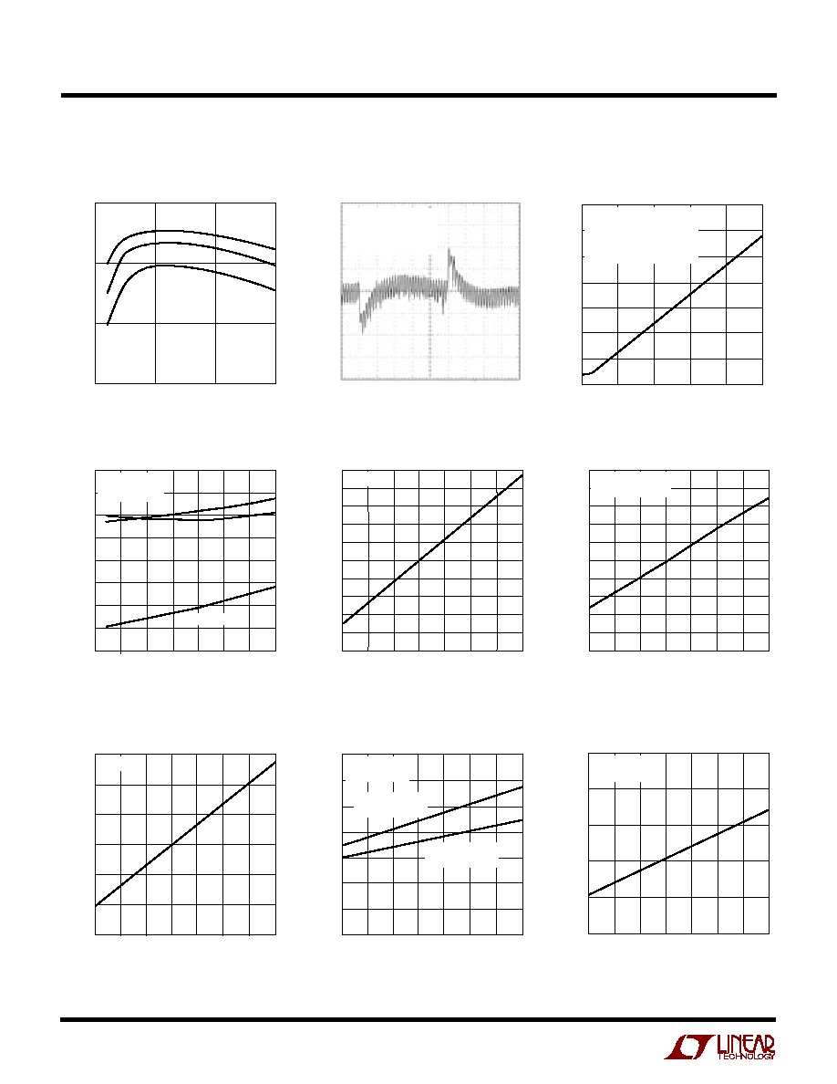
Efficiency vs Load Current
TEMPERATURE (
°
C)
50
SUPPLY CURRENT (mA)
2.4
PV
CC
V
CC
25
1703 G04
1.8
1.4
25
0
50
1.2
1.0
2.6
2.2
2.0
1.6
75
100
125
BOOST1, BOOST2
TEST CIRCUIT 1
C
L
= 0pF
Transient Response
TEMPERATURE (
°
C)
50
2.5
NORMALIZED FREQUENCY (%)
2.0
1.0
0.5
0
2.5
1.0
0
50
75
1703 G05
1.5
1.5
2.0
0.5
25
25
100
125
V
CC
= 5V
TEMPERATURE (
°
C)
50
0.4
R
ON
(
)
0.5
0.7
0.8
0.9
1.4
1.1
0
50
75
1703 G06
0.6
1.2
1.3
1.0
25
25
100
125
V
PVCC
= 5V
V
BOOST
V
SW
= 5V
MOSFET Driver Supply Current
vs Gate Capacitance
Supply Current vs Temperature
Normalized Frequency
vs Temperature
Driver R
ON
vs Temperature
RUN/SS Source Current
vs Temperature
TEMPERATURE (
°
C)
50
SOURCE CURRENT (
µ
A)
4.0
4.5
5.0
25
75
1703 G07
3.5
3.0
25
0
50
100
125
2.5
2.0
V
CC
= 5V
Nonoverlap Time vs Temperature
Driver Rise/Fall vs Temperature
LOAD CURRENT (A)
0
70
EFFICIENCY (%)
80
90
100
5
10
1703 G01
15
V
IN
= 5V
V
OUT
= 3.3V
V
OUT
= 2.5V
V
OUT
= 1.6V
V
IN
= 5V
V
OUT
= 1.8V
I
LOAD
= 0A-10A-0A
±
2.2% MAX DEVIATION
1703 G02
GATE CAPACITANCE (pF)
0
25
30
35
6000
8000
1703
G03
20
15
2000
4000
10000
10
5
0
DRIVER SUPPLY CURRENT (mA)
TEST CIRCUIT 1
ONE DRIVER LOADED
MULTIPLY BY # OF ACTIVE
DRIVERS TO OBTAIN TOTAL
DRIVER SUPPLY CURRENT
TEMPERATURE (
°
C)
50
40
50
70
25
75
1703 G08
30
20
25
0
50
100
125
10
0
60
NONOVERLAP (ns)
TEST CIRCUIT 1
C
L
= 2000pF
BG FALLING EDGE
TG RISING EDGE
TG FALLING EDGE
BG RISING EDGE
TEMPERATURE (
°
C)
50
25
12
RISE/FALL TIME (ns)
12
15
0
50
75
1703 G09
11
14
13
25
100
125
TEST CIRCUIT 1
C
L
= 2000pF
20mV/
DIV
10
µ
s/DIV
TYPICAL PERFOR A CE CHARACTERISTICS
U
W

5
LTC1703
FCB (Pin 7): Force Continuous Bar. The FCB pin forces
both converters to maintain continuous synchronous
operation regardless of load when the voltage at FCB
drops below 0.8V. FCB is normally tied to V
CC
. To force
continuous operation, tie FCB to SGND. FCB can also be
connected to a feedback resistor divider from a secondary
winding on one converter's inductor to generate a third
regulated output voltage. Do not leave FCB floating.
RUN/SS1 (Pin 8): Controller 1 Run/Soft-Start. Pulling
RUN/SS1 to SGND will disable controller 1 and turn off
both of its external MOSFET switches. Pulling both
RUN/SS pins down will shut down the entire LTC1703,
dropping the quiescent supply current below 100
µ
A. A
capacitor from RUN/SS1 to SGND will control the turn-on
time and rate of rise of the controller 1 output voltage at
power-up. An internal 3.5
µ
A current source pull-up at
RUN/SS1 pin sets the turn-on time at approximately
50ms/
µ
F.
COMP1 (Pin 9): Controller 1 Loop Compensation. The
COMP1 pin is connected directly to the output of the first
controller's error amplifier and the input to the PWM
comparator. An RC network is used at the COMP1 pin to
compensate the feedback loop for optimum transient
response.
SGND (Pin 10): Signal Ground. All internal low power
circuitry returns to the SGND pin. Connect to a low
impedance ground, separated from the PGND node. All
feedback, compensation and soft-start connections should
return to SGND. SGND and PGND should connect only at
a single point, near the PGND pin and the negative plate of
the C
IN
bypass capacitor.
FB1 (Pin 11): Controller 1 Feedback Input. The loop
compensation network for controller 1 should be con-
nected to FB1. FB1 is connected internally to the VID
resistor network to set the output voltage at side 1.
SENSE (Pin 12): Output Sense. Connect to V
OUT1
.
VID0 to VID4 (Pins 13 to 17): VID Programming Inputs.
These are logic inputs that set the output voltage at side 1
to a preprogrammed value (see Table 1). VID4 is the MSB,
VID0 is the LSB. The codes selected by the VID
n inputs
correspond to the Intel Mobile VID specification. Each
PV
CC
(Pin 1): Driver Power Supply Input. PV
CC
provides
power to the two BG
n output drivers. PV
CC
must be
connected to a voltage high enough to fully turn on the
external MOSFETs QB1 and QB2. PV
CC
should generally
be connected directly to V
IN
. PV
CC
requires at least a 1
µ
F
bypass capacitor directly to PGND.
BOOST1 (Pin 2): Controller 1 Top Gate Driver Supply. The
BOOST1 pin supplies power to the floating TG1 driver.
BOOST1 should be bypassed to SW1 with a 1
µ
F capacitor.
An additional Schottky diode from V
IN
to BOOST1 pin will
create a complete floating charge-pumped supply at
BOOST1. No other external supplies are required.
BG1 (Pin 3): Controller 1 Bottom Gate Drive. The BG1 pin
drives the gate of the bottom N-channel synchronous
switch MOSFET, QB1. BG1 is designed to drive up to
10,000pF of gate capacitance directly. If RUN/SS1 goes
low, BG1 will go low, turning off QB1. If FAULT mode is
tripped, BG1 will go high and stay high, keeping QB1 on
until the power is cycled.
TG1 (Pin 4): Controller 1 Top Gate Drive. The TG1 pin
drives the gate of the top N-channel MOSFET, QT1. The
TG1 driver draws power from the BOOST1 pin and returns
to the SW1 pin, providing true floating drive to QT1. TG1
is designed to drive up to 10,000pF of gate capacitance
directly. In shutdown or fault modes, TG1 will go low.
SW1 (Pin 5): Controller 1 Switching Node. SW1 should be
connected to the switching node of converter 1. The TG1
driver ground returns to SW1, providing floating gate
drive to the top N-channel MOSFET switch, QT1. The
voltage at SW1 is compared to I
MAX1
by the current limit
comparator while the bottom MOSFET, QB1, is on.
I
MAX1
(Pin 6): Controller 1 Current Limit Set. The I
MAX1
pin sets the current limit comparator threshold for
controller 1. If the voltage drop across the bottom MOSFET,
QB1, exceeds the magnitude of the voltage at I
MAX1
,
controller 1 will go into current limit. The I
MAX1
pin has an
internal 10
µ
A current source pull-up, allowing the current
threshold to be set with a single external resistor to PGND.
This current setting resistor should be Kelvin connected to
the source of QB1. See the Current Limit Programming
section for more information on choosing R
IMAX
.
U
U
U
PI FU CTIO S