Äîêóìåíòàöèÿ è îïèñàíèÿ www.docs.chipfind.ru
1
LTC1706-19
VID Voltage Programmer
1706-19 TA01
+
+
C
C
1000pF
50pF
R
C
10k
C
C2
220pF
C
SS
0.1
µ
F
C
OSC
47pF
R
F
4.7
1000pF
L1
3.3
µ
H
R
SENSE
0.015
V
IN
4.5V TO 22V
V
OUT
1.3V TO 2V
7A
0.22
µ
F
C
F
0.1
µ
F
C
IN
10
µ
F
30V
X2
4.7
µ
F
M1
Si4410
M2
Si4410
*D
B
*CMDSH-3
D1
MBRS140T3
+
C
OUT
820
µ
F
4V
X2
V
CC
FB
0 1 2
VID
LTC1706-19
FROM
µ
P
3
GND
SENSE
V
IN
INTV
CC
C
OSC
SGND
V
OSENSE
TG
SW
PGND
BG
BOOST
RUN/SS
I
TH
SENSE
+
SENSE
LTC1435A
13
1
16
2
3
14
12
8
7
5
15
11
10
6
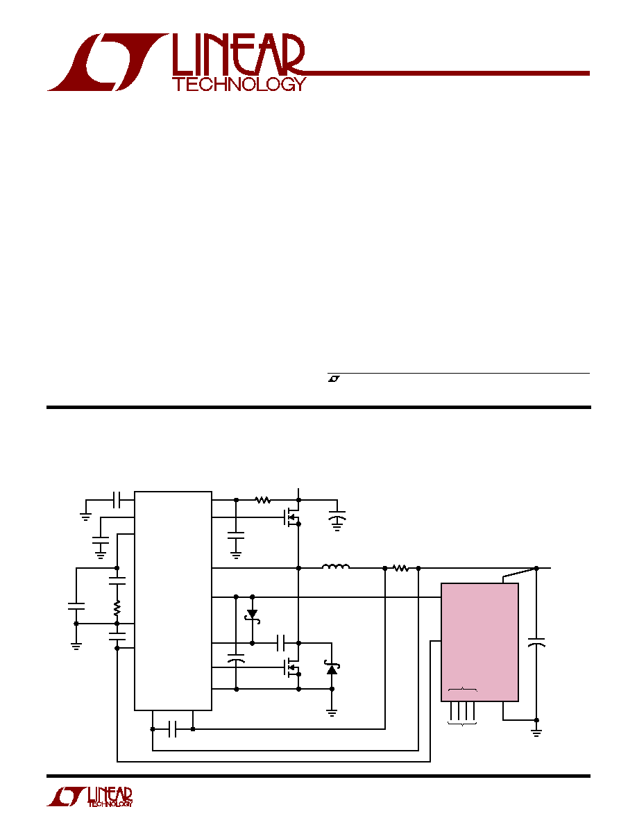
TYPICAL APPLICATIO
U
Intel Mobile Pentium II Processor Power Supply
s
Programs Regulator Output Voltage from 1.3V to
2V in 50mV Steps
s
Programs an Entire Family of Linear Technology
DC/DC Converters
s
Fully Compliant with the Intel Mobile VID
Specification
s
±
0.25% Accurate Output Voltage
s
Built-In 40k Pull-Up Resistors on VID Inputs
s
Available in SO-8 Packaging
FEATURES
The LTC
®
1706-19 is a precision, digitally programmed,
resistive ladder which adjusts the output of any 1.19V
referenced regulator. Depending on the state of the four
VID inputs, an output voltage between 1.3V and 2V is
programmed in 50mV increments.
The LTC1706-19 is designed specifically to program an
entire family of Linear Technology DC/DC converters in full
compliance with the Intel Mobile VID specification.
The LTC1706-19 programs the following Linear Technol-
ogy DC/DC converter products: LTC1433, LTC1434,
LTC1435, LTC1435A, LTC1436, LTC1437, LTC1438,
LTC1439, LTC1538-AUX, LTC1539, LTC1624 and
LTC1625. (Consult factory for future compatible DC/DC
converter products.)
DESCRIPTIO
U
APPLICATIO
N
S
U
s
Intel Mobile Pentium
®
II Processor Power Supply
s
Notebook and Palmtop Computers, PDAs
s
Portable Instruments
s
Battery-Powered Equipment
Pentium is a registered trademark of Intel Corporation.
, LTC and LT are registered trademarks of Linear Technology Corporation.
2
LTC1706-19
ABSOLUTE AXI U
RATI GS
W
W
W
U
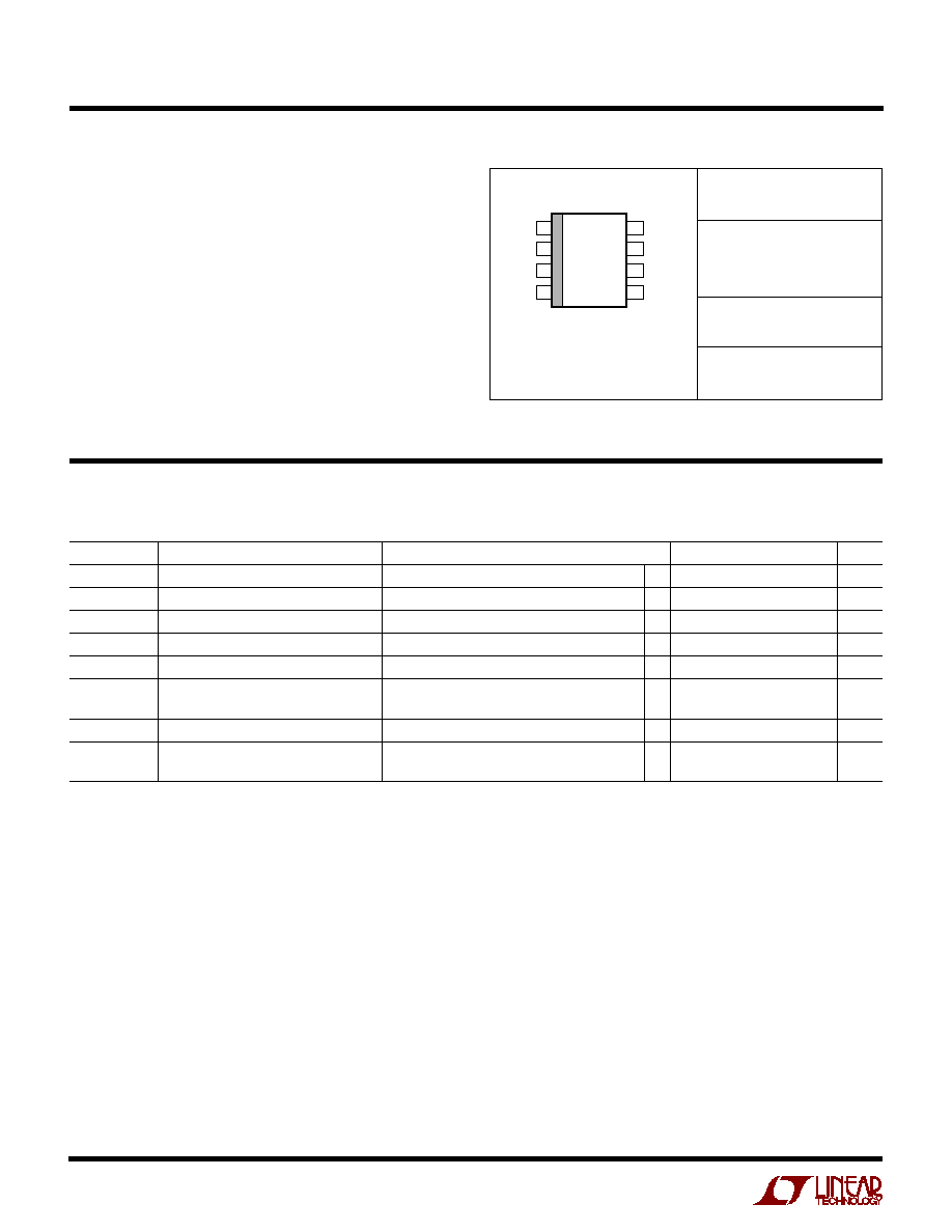
PACKAGE/ORDER I FOR ATIO
U
U
W
ORDER PART
NUMBER
LTC1706CS8-19
LTC1706IS8-19
1
2
3
4
8
7
6
5
TOP VIEW
VID1
VID0
SENSE
FB
VID2
VID3
V
CC
GND
S8 PACKAGE
8-LEAD PLASTIC SO
T
JMAX
= 110
°
C,
JA
= 120
°
C/W
Consult factory for Military grade parts.
ELECTRICAL CHARACTERISTICS
T
A
= 25
°
C, 2.7V
V
CC
5.5V, VID0 = VID1 = VID2 = VID3 = N. C., unless otherwise specified.
SYMBOL
PARAMETER
CONDITIONS
MIN
TYP
MAX
UNITS
V
CC
Operating Supply Voltage Range
2.7
5.5
V
I
VCC
Supply Current
(Note 2)
0.1
5
µ
A
R
FB-SENSE
Resistance Between SENSE and FB
q
8
15
20
k
V
OUT
Error %
Output Voltage Accuracy
Programmed From 1.3V to 2V
q
0.25
0.25
%
R
PULLUP
VID Input Pull-Up Resistance
V
DIODE
= 0.6V, V
CC
= 5V, (Note 3)
40
k
VID
T
VID Input Voltage Threshold
V
IL
(2.7V
V
CC
5.5V)
0.4
V
V
IH
(2.7V
V
CC
5.5V)
1.6
V
I
VID-LEAK
VID Input Leakage Current
V
CC
< VID < 7V, (Note 3)
0.01
±
1
µ
A
V
PULLUP
VID Pull-Up Voltage
V
CC
= 3.3V
2.8
V
V
CC
= 5V
4.5
V
The
q
denotes specifications which apply over the full specified
temperature range.
Note 1: Absolute Maximum Ratings are those values beyond which the life
of a device may be impaired.
Note 2: With all four VID inputs floating, the V
CC
supply current is simply
the device leakage current. However, the V
CC
supply current will rise and
be approximately equal to the number of grounded VID input pins times
(V
CC
0.6V)/40k. (See the Typical Applications section for more detail.)
Note 3: Each built-in pull-up resistor attached to the VID inputs also has a
series diode connected to V
CC
to allow input voltages higher than the V
CC
supply without damage or clamping. (See Operation section for further
detail.)
S8 PART
MARKING
170619
706I19
(Note 1)
(Voltages Referred to GND Pin)
Input Supply Voltage (V
CC
) .......................... 0.3V to 7V
VID Input Pins ............................................. 0.3V to 7V
SENSE Pin ................................................... 0.3V to 7V
FB Pin .......................................................... 0.3V to 7V
Operating Temperature Range
LTC1706C-19 .......................................... 0
°
C to 70
°
C
LTC1706I-19 ...................................... 40
°
C to 85
°
C
Junction Temperature ........................................... 110
°
C
Storage Temperature Range ................. 65
°
C to 150
°
C
Lead Temperature (Soldering, 10 sec).................. 300
°
C
3
LTC1706-19
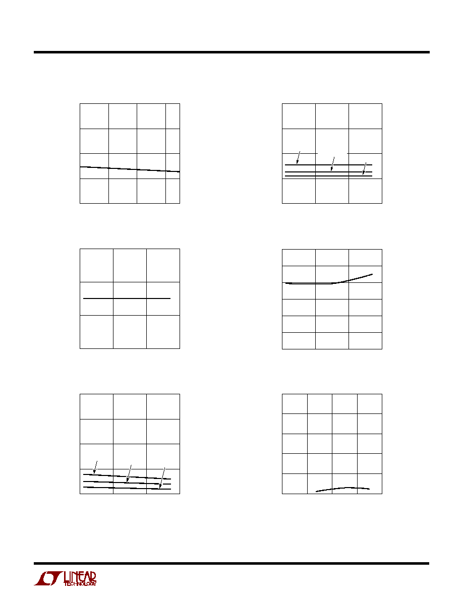
TYPICAL PERFOR A CE CHARACTERISTICS
U
W
OUTPUT VOLTAGE (V)
1.3
1.5
1.7
1.9
2.0
ERROR (%)
1706-19 G01
0.25
0
0.25
TEMPERATURE (
°
C)
50
0
50
100
ERROR (%)
1706-19 G02
0.25
0
0.25
V
OUT
= 2V
V
OUT
= 1.7V
V
OUT
= 1.3V
Typical Error % vs Output Voltage
Typical Error % vs Temperature
TEMPERATURE (
°
C)
50
0
50
100
R
FB1
(k
)
1706-19 G03
30
20
10
0
TEMPERATURE (
°
C)
50
0
50
100
VID PULL-UP CURRENT (
µ
A)
1706-19 G04
120
100
80
60
40
20
0
V
CC
= 5V
R
FB1
vs Temperature
I
VID-PULLUP
vs Temperature
TEMPERATURE (
°
C)
50
0
50
100
SUPPLY CURRENT (
µ
A)
1706-19 G05
2.0
1.5
1.0
0.5
0
V
CC
= 2.7V
V
CC
= 5V
V
CC
= 3.3V
SUPPLY VOLTAGE (V)
0
2
4
6
8
SUPPLY CURRENT (
µ
A)
1706-19 G06
5
4
3
2
1
0
Supply Current vs Temperature
Supply Current vs Supply Voltage
4
LTC1706-19
PI FU CTIO S
U
U
U
VID2 (Pin 1): 2nd MSB Programming Input. Low = GND,
High = V
CC
or Float. Grounding VID2 adds 200mV to the
output sense voltage.
VID3 (Pin 2): 1st MSB Programming Input. Low = GND,
High = V
CC
or Float. Grounding VID3 adds 400mV to the
output sense voltage.
V
CC
(Pin 3): Power Supply Voltage. Range from 2.7V to
5.5V.
GND (Pin 4): Ground. Connect to regulator signal ground.
FB (Pin 5): Feedback Input. Connect to the 1.19V feedback
pin of a compatible regulator.
SENSE (Pin 6): Regulator Output Voltage. Connect di-
rectly to regulator output sense node.
VID0 (Pin 7): LSB Programming Input. Low = GND,
High = V
CC
or Float. Grounding VID0 adds 50mV to the
output sense voltage.
VID1 (Pin 8): 3rd MSB Programming Input. Low = GND,
High = V
CC
or Float. Grounding VID1 adds 100mV to the
output sense voltage.
BLOCK DIAGRA
W
NOMINAL (V)
ABSOLUTE MAX (V)
PIN
NAME
DESCRIPTION
MIN
TYP
MAX
MIN
MAX
1
VID2
2nd MSB Programmable Input
0
V
CC
0.3
7
2
VID3
1st MSB Programmable Input
0
V
CC
0.3
7
3
V
CC
Power Supply
2.7
5.5
0.3
7
4
GND
Ground
0
0
0
5
FB
1.19V Feedback Input
0
1.19
1.5
0.3
7
6
SENSE
Regulator Output Voltage
1.3
2
0.3
7
7
VID0
LSB Programmable Input
0
V
CC
0.3
7
8
VID1
3rd MSB Programmable Input
0
V
CC
0.3
7
1706-19 BD
40k
VID3
V
CC
40k
VID2
V
CC
40k
VID1
V
CC
SWITCH
CONTROL
LOGIC
40k
VID0
V
CC
R
FB2
R
FB1
SENSE
FB
GND
V
CC
5
LTC1706-19
OPERATIO
U
The LTC1706-19 is a precision resistive divider designed
specifically for use with an entire family of Linear Technol-
ogy Corporation DC/DC switching regulators with 1.19V
internal reference and feedback voltages. The LTC1706-19
produces an output voltage ranging from 1.3V to 2V in
50mV steps by closing the loop between the output
voltage sense and the feedback input of the regulator with
the appropriate resistive divider network.
The "top" feedback resistor, R
FB1
, connected between
SENSE and FB, is typically 15k and is not modified by the
state of the VID program inputs. However, the "bottom"
feedback resistor, R
FB2
, is modified by the four VID inputs
and is precisely ratioed to R
FB1
.
VID Programming
Programming is accomplished by applying the proper
voltage (or float condition) on the four digital VID inputs.
VID3 is the most significant bit (MSB), and VID0 is the
least significant bit (LSB). When all four inputs are low, or
grounded, the regulator output voltage is set to 2V. Each
increasing binary count is equivalent to a decrease of
50mv in the output voltage. Therefore, to obtain a 1.3V
output, the three MSBs are left floating, or high, while only
the LSB, VID0, is grounded. A list of programmed inputs
and their corresponding output voltages is shown in
Table 1.
When all four VID inputs are high or floating (1111), such
as when no CPU is present in a system, a regulated 1.25V
output is generated at V
SENSE
.
Each VID
input pin is pulled up by a 40k resistor in series
with a diode connected to V
CC
. Therefore, it should be
grounded (or driven low) to produce a digital low input. It
can be either floated or connected to V
CC
to get a digital
high input. The series diode is included to prevent the
input from being damaged or clamped if it is driven higher
than V
CC
.
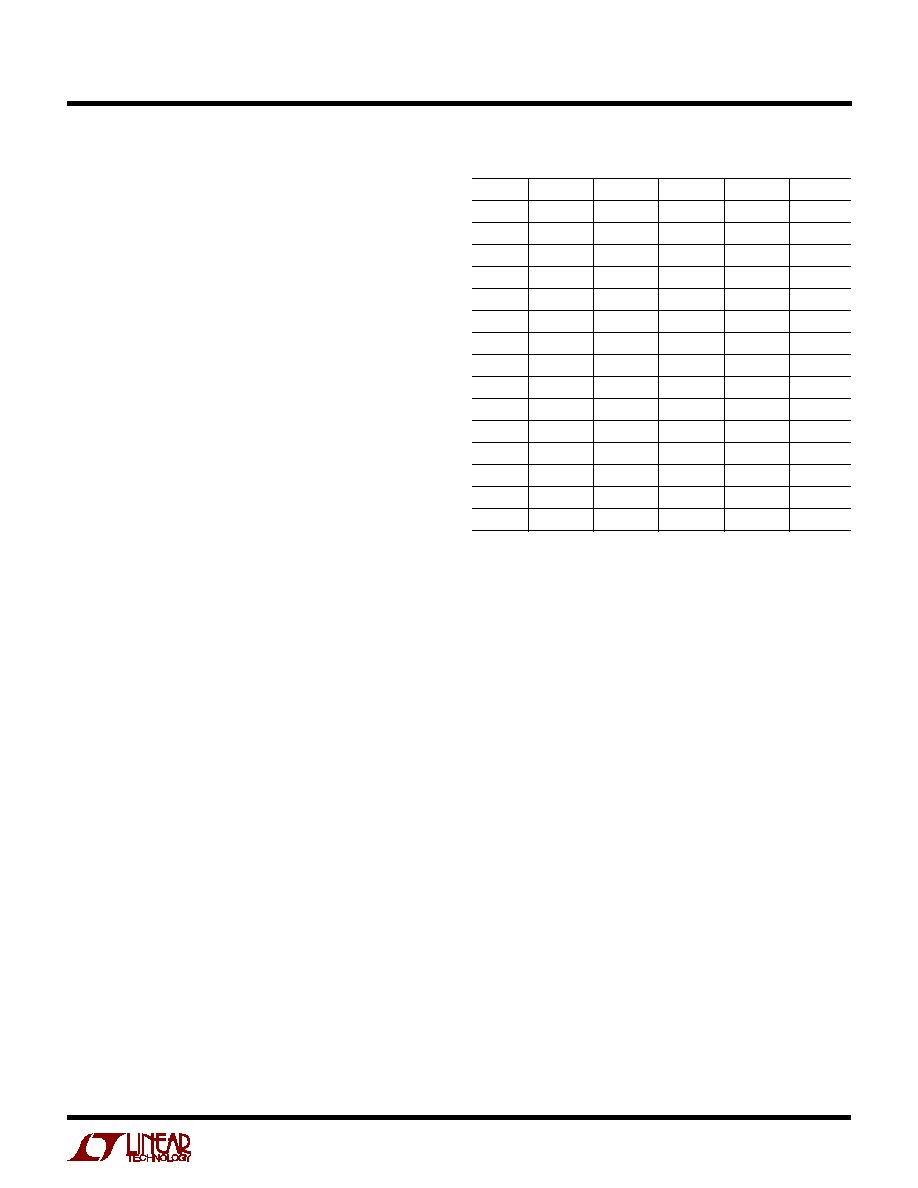
Table 1. VID Inputs and Corresponding Output Voltage
CODE
VID3
VID2
VID1
VID0
OUTPUT
0000
GND
GND
GND
GND
2.00V
0001
GND
GND
GND
Float
1.95V
0010
GND
GND
Float
GND
1.90V
0011
GND
GND
Float
Float
1.85V
0100
GND
Float
GND
GND
1.80V
0101
GND
Float
GND
Float
1.75V
0110
GND
Float
Float
GND
1.70V
0111
GND
Float
GND
GND
1.65V
1000
Float
GND
GND
GND
1.60V
1001
Float
GND
GND
Float
1.55V
1010
Float
GND
Float
GND
1.50V
1011
Float
GND
Float
Float
1.45V
1100
Float
Float
GND
GND
1.40V
1101
Float
Float
GND
Float
1.35V
1110
Float
Float
Float
GND
1.30V
Voltage Sensing and Feedback Pins
The FB pin is a high impedance node that requires mini-
mum layout distance to reduce extra loading and
unwanted stray pickup.
When used with the LTC1435A, the LTC1706-19's FB,
SENSE, V
CC
and GND pins should be connected, respec-
tively, with the V
OSENSE
, V
OUT
, INTV
CC
and SGND pins of
the LTC1435A. The result of this application is a precisely
controlled variable voltage supply for any low voltage
system such as a palmtop or a laptop computer.