Äîêóìåíòàöèÿ è îïèñàíèÿ www.docs.chipfind.ru
1
LTC1708-PG
Dual Adjustable 5-Bit VID
High Efficiency, 2-Phase Current Mode
Synchronous Buck Regulator Controller
February 2000
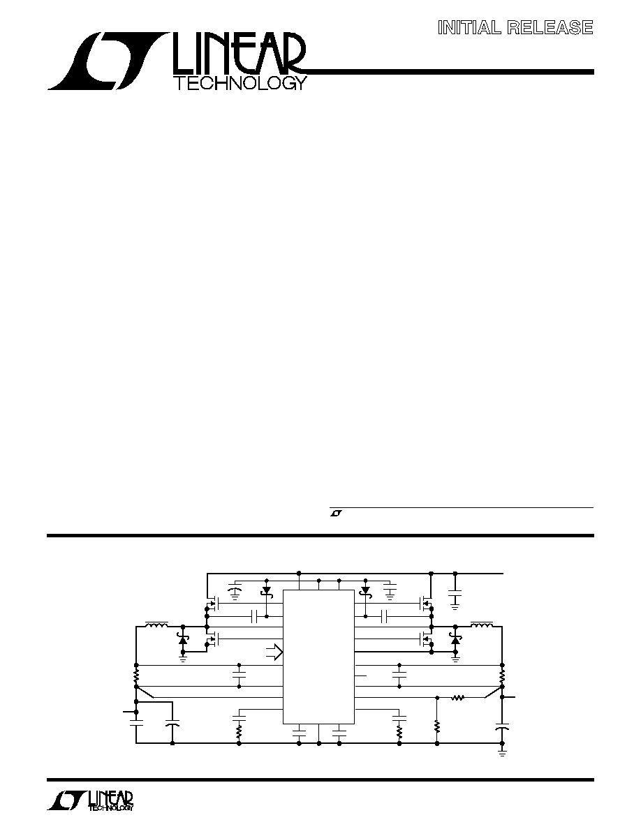
Figure 1. High Efficiency VID Controlled, 2-Output Step-Down Converter
s
Out-of-Phase Controllers Reduce Input Capacitance
and Power Supply Induced Noise
s
OPTI-LOOP
TM
Compensation Minimizes C
OUT
s
Power Good Output Monitors Both Outputs
s
5-Bit Mobile VID Control, V
OUT
: 0.9V to 2.0V
s
Dual N-Channel MOSFET Synchronous Drive
s
±
1% Output Voltage Accuracy
s
DC Programmed Fixed Frequency 150kHz to 300kHz
s
Wide V
IN
Range: 3.5V to 36V Operation
s
Very Low Dropout Operation: 99% Duty Cycle
s
Adjustable Soft-Start Current Ramping
s
Foldback Output Current Limiting
s
Latched Short-Circuit Shutdown with Defeat Option
s
Output Overvoltage Protection
s
Remote Output Voltage Sense
s
Low Shutdown Current: 20
µ
A
s
5V and 3.3V Standby Regulators
s
Selectable Constant Frequency, Burst Mode
TM
and
Continuous Operation
The LTC
®
1708 is a dual adjustable 5-bit VID program-
mable step-down switching regulator controller that drives
all N-Channel power MOSFET stages. A constant fre-
quency current mode architecture allows adjustment of
the frequency up to 300kHz. Power loss and noise due to
the ESR of the input capacitance are minimized by oper-
ating the two main controller output stages out of phase.
OPTI-LOOP compensation allows the transient response
to be optimized over a wide range of output capacitance
and ESR values. The precision 0.8V reference is compat-
ible with future microprocessor generations, and a wide
3.5V to 30V (36V maximum) input supply range that
encompasses all battery chemistries. A power good out-
put indicates when the output voltages are within 7.5% of
their programmed value.
A RUN/SS pin for each controller provides both soft-start
and an optional timed, short-circuit shutdown. Other
protection features include: internal foldback current lim-
iting and an output overvoltage crowbar. The force con-
tinuous control pin (FCB) can be used to inhibit Burst
Mode operation or to regulate a third, flyback output.
s
Notebook and Palmtop Computers, PDAs
s
Portable Instruments
, LTC and LT are registered trademarks of Linear Technology Corporation.
Burst Mode and OPTI-LOOP are trademarks of Linear Technology Corporation.
+
4.7
µ
F
D3
D4
D1
M2
5 VID BITS
M1
C
B1
0.47
µ
F
1000pF
L1
1
µ
H
C
C1
1500pF
1
µ
F
CERAMIC
C
IN
10
µ
F
50V
CERAMIC
×
4
C
OUT1
270
µ
F
2V
SP
×
4
C
OUT1a
10
µ
F
6.3V
CERAMIC
R
SENSE1
0.003
R
C1
22k
V
OUT1
0.925V TO
2.00V
14.1A
D2
M3b
M3a
C
B2
0.1
µ
F
R4
63.4k
1%
L2
2.2
µ
H
C
C2
220pF
1000pF
+
C
OUT
180
µ
F
4V
SP
R
SENSE2
0.01
R3
20k
1%
R
C2
15k
V
OUT2
1.5V
4A
TG1
TG2
BOOST1
BOOST2
SW1
SW2
BG1
BG2
VID0 TO VID4
PGND
SENSE1
+
SENSE2
+
SENSE1
SENSE2
PGOOD
ATTNIN
V
OSENSE2
I
TH1
I
TH2
V
IN
VIDV
CC
INTV
CC
RUN/SS1
RUN/SS2
SGND
V
IN
4.75V TO 28V
M1: IRF7811
M2: 1RF7809
M3a, M3b: FDS6982
L1: VISHAY 5050CE
ATTNOUT CONNECTED TO EAIN1
1628 F01
C
SS1
0.1
µ
F
C
SS2
0.1
µ
F
LTC1708-PG
+
DESCRIPTIO
U
FEATURES
APPLICATIO S
U
TYPICAL APPLICATIO
U
Final Electrical Specifications
Information furnished by Linear Technology Corporation is believed to be accurate and reliable.
However, no responsibility is assumed for its use. Linear Technology Corporation makes no represen-
tation that the interconnection of its circuits as described herein will not infringe on existing patent rights.
2
LTC1708-PG
T
JMAX
= 125
°
C,
JA
= 85
°
C/W
1
2
3
4
5
6
7
8
9
10
11
12
13
14
15
16
17
18
TOP VIEW
G PACKAGE
36-LEAD PLASTIC SSOP
36
35
34
33
32
31
30
29
28
27
26
25
24
23
22
21
20
19
RUN/SS1
SENSE1
+
SENSE1
EAIN1
FREQSET
STBYMD
FCB
I
TH1
SGND
3.3V
OUT
I
TH2
EAIN2
SENSE2
SENSE2
+
ATTNOUT
ATTNIN
VID0
VID1
PGOOD
TG1
SW1
BOOST1
V
IN
BG1
EXTV
CC
INTV
CC
PGND
BG2
BOOST2
SW2
TG2
RUN/SS2
VIDV
CC
VID4
VID3
VID2
ORDER PART
NUMBER
LTC1708EG-PG
ABSOLUTE AXI U
RATI GS
W
W
W
U
PACKAGE/ORDER I FOR ATIO
U
U
W
(Note 1)
Input Supply Voltage (V
IN
).........................36V to 0.3V
Topside Driver Voltages
(BOOST1, BOOST2) ...................................42V to 0.3V
Switch Voltage (SW1, SW2) .........................36V to 5V
INTV
CC,
EXTV
CC
, RUN/SS1, RUN/SS2,
(BOOST1-SW1), (BOOST2-SW2), ...............7V to 0.3V
SENSE1
+
, SENSE2
+
, SENSE1
,
SENSE2
Voltages ....................... (1.1)INTV
CC
to 0.3V
FREQSET, STBYMD, FCB, VIDV
CC
, VID0-4,
PGOOD Voltages .......................................... 7V to 0.3V
I
TH1,
I
TH2
, EAIN1, EAIN2, ATTNIN,
ATTNOUT Voltages ................................... 2.7V to 0.3V
Peak Output Current <10
µ
s (TG1, TG2, BG1, BG2) ... 3A
INTV
CC
Peak Output Current ................................ 50mA
Operating Ambient Temperature Range
(Note 2) ...................................................40
°
C to 85
°
C
Junction Temperature (Note 3) ............................. 125
°
C
Storage Temperature Range ................. 65
°
C to 150
°
C
Lead Temperature (Soldering, 10 sec).................. 300
°
C
Consult factory for Industrial and Military grade parts.
ELECTRICAL CHARACTERISTICS
The
q
denotes the specifications which apply over the full operating
SYMBOL
PARAMETER
CONDITIONS
MIN
TYP
MAX
UNITS
Main Control Loops
V
EAIN1, 2
Regulated Feedback Voltage
(Note 4); I
TH1, 2
Voltage = 1.2V
q
0.792
0.800
0.808
V
at EAIN Pin
I
EAIN1, 2
Feedback Current
(Note 4)
5
50
nA
V
REFLNREG
Reference Voltage Line Regulation
V
IN
= 3.6V to 30V (Note 4)
0.002
0.02
%/V
V
LOADREG
Output Voltage Load Regulation
(Note 4)
Measured in Servo Loop; I
TH1, 2
Voltage = 1.2V to 0.7V
q
0.1
0.5
%
Measured in Servo Loop; I
TH1, 2
Voltage = 1.2V to 2.0V
q
0.1
0.5
%
g
m1, 2
Transconductance Amplifier g
m
I
TH1, 2
= 1.2V; Sink/Source 5
µ
A; (Note 4)
1.3
mmho
g
mOL1, 2
Transconductance Amplifier GBW
I
TH1, 2
= 1.2V; (g
m
· Z
L
, No Ext Load) (Note 4)
3
MHz
I
Q
Input DC Supply Current
(Note 5)
Normal Mode
EXTV
CC
Tied to GND; VID Inputs Open Circuit
850
µ
A
Standby
V
RUN/SS1, 2
= 0V, V
STBYMD
> 2V
125
µ
A
Shutdown
V
RUN/SS1, 2
= 0V, V
STBYMD
= Open
20
35
µ
A
V
FCB
Forced Continuous Threshold
q
0.760
0.800
0.840
V
I
FCB
Forced Continuous Current
V
FCB
= 0.85V
0.3
0.18
0.1
µ
A
V
BINHIBIT
Burst Inhibit Threshold
Measured at FCB pin
4.3
4.8
V
UVLO
Undervoltage Lockout
V
IN
Ramping Down
3.5
4
V
temperature range, otherwise specifications are at T
A
= 25
°
C. V
IN
= 15V, V
RUN/SS1, 2
= 5V unless otherwise noted.
3
LTC1708-PG
ELECTRICAL CHARACTERISTICS
The
q
denotes the specifications which apply over the full operating
temperature range, otherwise specifications are at T
A
= 25
°
C. V
IN
= 15V, V
RUN/SS1, 2
= 5V unless otherwise noted.
SYMBOL
PARAMETER
CONDITIONS
MIN
TYP
MAX
UNITS
V
OV
Output Overvoltage Threshold
Measured at EAIN1, 2
0.84
0.86
0.88
V
I
SENSE
Sense Pins Total Source Current
(Each Channel); V
SENSE1
, 2
= V
SENSE1
+
, 2
+
= 0V
85
60
µ
A
V
STBYMD
MS
Master Shutdown Threshold
V
STBYMD
Ramping Down
0.4
0.6
V
V
STBYMD
KA
Keep-Alive Power On-Threshold
V
STBYMD
Ramping Up, RUN
SS1, 2
= 0V
1.5
2
V
DF
MAX
Maximum Duty Factor
In Dropout
98
99.4
%
I
RUN/SS1, 2
Soft-Start Charge Current
V
RUN/SS1, 2
= 1.9V
0.5
1.2
µ
A
V
RUN/SS1, 2
ON RUN/SS Pin ON Threshold
V
RUN/SS1,
V
RUN/SS2
Rising
1.0
1.5
1.9
V
V
RUN/SS1, 2
LT
RUN/SS Pin Latchoff Threshold
V
RUN/SS1,
V
RUN/SS2
Rising from 3V
4.1
4.5
V
I
SCL1, 2
RUN/SS Discharge Current
Soft Short Condition E
AIN1, 2
= 0.5V;
0.5
2
4
µ
A
V
RUN/SS1, 2
= 4.5V
I
SDLHO
Shutdown Latch Disable Current
EAIN1, 2
= 0.5V
1.6
5
µ
A
V
SENSE(MAX)
Maximum Current Sense Threshold
V
EAIN1, 2
= 0.7V; V
SENSE1, 2
= 5V
65
75
85
mV
V
EAIN1, 2
= 0.7V; V
SENSE1, 2
= 5V
q
62
75
88
mV
TG Transition Time:
TG1, 2 t
r
Rise Time
C
LOAD
= 3300pF (Note 10)
50
90
ns
TG1, 2 t
f
Fall Time
C
LOAD
= 3300pF (Note 10)
50
90
ns
BG Transition Time:
BG1, 2 t
r
Rise Time
C
LOAD
= 3300pF (Note 10)
40
90
ns
BG1, 2 t
f
Fall Time
C
LOAD
= 3300pF (Note 10)
40
80
ns
TG/BG t
1D
Top Gate Off to Bottom Gate On Delay
C
LOAD
= 3300pF Each Driver (Note 10)
90
ns
Synchronous Switch-On Delay Time
BG/TG t
2D
Bottom Gate Off to Top Gate On Delay
C
LOAD
= 3300pF Each Driver (Note 10)
90
ns
Top Switch-On Delay Time
t
ON(MIN)
Minimum On-Time
Tested with a Square Wave (Notes 6, 10)
160
200
ns
INTV
CC
Linear Regulator
V
INTVCC
Internal V
CC
Voltage
6V < V
IN
< 30V, V
EXTVCC
= 4V
4.8
5.0
5.2
V
V
LDO
INT
INTV
CC
Load Regulation
I
CC
= 0 to 20mA, V
EXTVCC
= 4V
0.2
1.0
%
V
LDO
EXT
EXTV
CC
Voltage Drop
I
CC
= 20mA, V
EXTVCC
= 5V
120
240
mV
V
EXTVCC
EXTV
CC
Switchover Voltage
I
CC
= 20mA, EXTV
CC
Ramping Positive
q
4.5
4.7
V
V
LDOHYS
EXTV
CC
Hysteresis
0.2
V
Oscillator
f
OSC
Oscillator Frequency
V
FREQSET
= Open (Note 7)
190
220
250
kHz
f
LOW
Lowest Frequency
V
FREQSET
= 0V
120
140
170
kHz
f
HIGH
Highest Frequency
V
FREQSET
= 2.4V
280
310
350
kHz
I
FREQSET
FREQSET
Input Current
V
FREQSET
= 0V
2
1
µ
A
3.3V Linear Regulator
V
3.3OUT
3.3V Regulator Output Voltage
No Load
q
3.25
3.35
3.45
V
V
3.3IL
3.3V Regulator Load Regulation
I
3.3
= 0 to 10mA
0.5
2
%
V
3.3VL
3.3V Regulator Line Regulation
6V < V
IN
< 30V
0.05
0.2
%
PGOOD Output
V
PGL
PGOOD Voltage Low
I
PGOOD
= 2mA
0.1
0.3
V
I
PGOOD
PGOOD Leakage Current
V
PGOOD
= 5V
1
µ
A
V
PG
PGOOD Trip Level
Relative to the 0.8V Regulated Feedback Voltage
EAIN1, 2 Ramping Negative from 0.8V
10
7.5
5
%
EAIN1, 2 Ramping Positive from 0.8V
5
7.5
10
%
4
LTC1708-PG
Note 1: Absolute Maximum Ratings are those values beyond which the life
of a device may be impaired.
Note 2: The LTC1708EG-PG is guaranteed to meet performance
specifications from 0
°
C to 70
°
C. Specifications over the 40
°
C to 85
°
C
operating temperature range are assured by design, characterization and
correlation with statistical process controls.
Note 3: T
J
is calculated from the ambient temperature T
A
and power
dissipation P
D
according to the following formulas:
LTC1708EG-PG: T
J
= T
A
+ (P
D
· 85
°
C/W)
Note 4: The LTC1708-PG is tested in a feedback loop that servos V
ITH1, 2
to a specified voltage and measures the resultant EAIN1, 2.
Note 5: The supply current is higher due to the gate charge being delivered
at the switching frequency. See Applications Information.
ELECTRICAL CHARACTERISTICS
The
q
denotes the specifications which apply over the full operating
temperature range, otherwise specifications are at T
A
= 25
°
C. V
IN
= 15V, V
RUN/SS1, 2
= 5V unless otherwise noted.
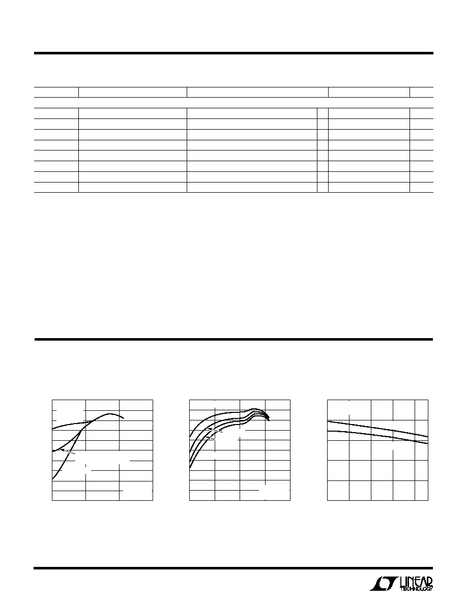
TYPICAL PERFOR A CE CHARACTERISTICS
U
W
Efficiency vs Output Current
and Mode (Figure 12)
OUTPUT CURRENT (A)
0.1
0
EFFICIENCY (%)
20
30
40
50
60
70
1
10
15A
1708 G01
80
90
100
10
100
Burst Mode
OPERATION
CONSTANT FREQUENCY
MODE
PWM MODE
V
IN
= 15V
V
OUT
= 1.6V
OUTPUT CURRENT (A)
0.01
EFFICIENCY (%)
40
60
100
1708
G02
20
0
0.1
1
10
100
80
30
50
15A
10
90
70
V
IN
= 10V
V
IN
= 15V
V
IN
= 5V
V
FCB
= OPEN
V
OUT
= 1.6V
V
IN
= 20V
EXTV
CC
= 0V
INPUT VOLTAGE (V)
5
10
EFFICIENCY (%)
70
80
1708
G03
60
50
15
20
25
28
100
90
V
OUT
= 1.6V
EXTV
CC
= 0V
I
OUT
= 7A
I
OUT
= 12A
Efficiency vs Output Current
(Figure 12)
Efficiency vs Input Voltage
(Figure 12)
Note 6: The minimum on-time condition corresponds to the on inductor
peak-to-peak ripple current
40% of I
MAX
(see minimum on-time
considerations in the Applications Information section).
Note 7: V
FREQSET
pin internally tied to 1.19V reference through a large
resistance.
Note 8: With all five VID inputs floating (or tied to VIDV
CC
) the VIDV
CC
current is typically < 1
µ
A. However, the VIDV
CC
current will rise and be
approximately equal to the number of grounded VID input pins times
(VIDV
CC
0.6V)/40k. (See the Applications Information section.)
Note 9: Each built-in pull-up resistor attached to the VID inputs also has a
series diode to allow input voltages higher than the VIDV
CC
supply without
damage or clamping. (See Applications Information section.)
Note 10: Rise and fall times are measured at 20% to 80% levels. Delay
and nonoverlap times are measured using 50% levels.
SYMBOL
PARAMETER
CONDITIONS
MIN
TYP
MAX
UNITS
VID Parameters
VIDV
CC
VID Operating Supply Voltage
2.7
5.5
V
I
VIDVCC
VID Supply Current
VIDV
CC
= 3.3V (Note 8)
0.01
5
µ
A
R
FBOUT1/SENSE1
Resistance Between ATTNIN/ATTNOUT
10
5
k
R
RATIO
Resistor Ratio Accuracy
Programmed from 0.925V to 2.00V
0.25
%
R
PULL-UP
VID0 to VID4 Pull-Up Resistance
(Note 9) V
DIODE
= 0.7V
40
k
V
IDT
VID Voltage Threshold
0.4
1.0
1.6
V
I
VIDLEAK
VID Input Leakage Current
(Note 9) VIDV
CC
< VIDV
CC
< 7V
0.1
1
µ
A
V
PULL-UP
VID Pull-Up Voltage
VIDV
CC
= 3V
2.5
2.8
3.1
V
5
LTC1708-PG
TYPICAL PERFOR A CE CHARACTERISTICS
U
W
Internal 5V LDO Line Reg
Maximum Current Sense Threshold
vs Duty Factor
Maximum Current Sense Threshold
vs Percent of Nominal Output
Voltage (Foldback)
INPUT VOLTAGE (V)
0
4.8
4.9
5.1
15
25
1708 G07
4.7
4.6
5
10
20
30
35
4.5
4.4
5.0
INTV
CC
VOLTAGE (V)
I
LOAD
= 1mA
DUTY FACTOR (%)
0
0
V
SENSE
(mV)
25
50
75
20
40
60
80
1708 G08
100
PERCENT ON NOMINAL OUTPUT VOLTAGE (%)
0
V
SENSE
(mV)
40
50
60
100
1708 G09
30
20
0
25
50
75
10
80
70
Maximum Current Sense Threshold
vs V
RUN/SS
(Soft-Start)
V
RUN/SS
(V)
0
0
V
SENSE
(mV)
20
40
60
80
1
2
3
4
1708 G10
5
6
V
SENSE(CM)
= 1.6V
Maximum Current Sense Threshold
vs Sense Common Mode Voltage
COMMON MODE VOLTAGE (V)
0
V
SENSE
(mV)
72
76
80
4
1708 G11
68
64
60
1
2
3
5
Current Sense Threshold
vs I
TH
Voltage
V
ITH
(V)
0
V
SENSE
(mV)
30
50
70
90
2
1708
G12
10
10
20
40
60
80
0
20
30
0.5
1
1.5
2.5
INTV
CC
and EXTV
CC
Switch
Voltage vs Temperature
Supply Current vs Input Voltage
and Mode (Figure 12)
INPUT VOLTAGE (V)
0
5
0
SUPPLY CURRENT (
µ
A)
400
1000
10
20
25
1708 G04
200
800
600
15
30
35
BOTH
CONTROLLERS ON
STANDBY
SHUTDOWN
EXTV
CC
Voltage Drop
CURRENT (mA)
0
EXTV
CC
VOLTAGE DROP (mV)
150
200
250
40
1708 G05
100
50
0
10
20
30
50
TEMPERATURE (
°
C)
50
INTV
CC
AND EXTV
CC
SWITCH VOLTAGE (V)
4.95
5.00
5.05
25
75
1708
G06
4.90
4.85
25
0
50
100
125
4.80
4.70
4.75
INTV
CC
VOLTAGE
EXTV
CC
SWITCHOVER THRESHOLD