17278i.pm6
1
LTC1727/LTC1728
17278fa
Micropower Precision
Triple Supply Monitors
in 8-Lead MSOP and
5-Lead SOT-23 Packages
s
Monitors Three Inputs Simultaneously
LTC1727-5: 5V, 3.3V and ADJ
LTC1727-2.5: 2.5V, 3.3V and ADJ
LTC1728-5: 5V, 3.3V and ADJ
LTC1728-2.5: 2.5V, 3.3V and ADJ
LTC1728-1.8: 3V, 1.8V and ADJ
LTC1728-3.3: 3.3V, 1.8V and ADJ
s
±
1.5% Threshold Accuracy Over Temperature
s
Very Low Supply Current: 10
µ
A Typ
s
200ms Reset Time Delay
s
Active Low RESET Output
s
Power Supply Glitch Immunity
s
Guaranteed RESET for V
CC3
1V
or V
CC5
/V
CC25
/V
CC18
1V
s
LTC1727 Includes Monitor Output for Each Supply
s
LTC1727: 8-Lead MSOP and SO Packages
s
LTC1728: 5-Lead SOT-23 Package
The LTC
®
1727 is a triple supply monitor intended for
systems with multiple supply voltages. Each supply moni-
tor has its own open-drain output for individual supply
monitoring. A common open-drain reset output remains
low until all three supplies have been in compliance for
200ms. Tight 1.5% accuracy specifications and glitch
immunity ensure reliable reset operation without false
triggering.
The LTC1728 is functionally identical to the LTC1727
without the individual monitor outputs.
The RST output is guaranteed to be in the correct state for
V
CC5
/V
CC25
/V
CC18
or V
CC3
down to 1V. The LTC1727/
LTC1728 may also be configured to monitor any one or
two V
CC
inputs instead of three, depending on system
requirements.
Very low (10
µ
A typical) supply current makes the LTC1727/
LTC1728 ideal for power conscious systems.
The LTC1727 is available in an 8-lead MSOP or SO
package and the LTC1728 is available in a 5-lead SOT-23
package.
, LTC and LT are registered trademarks of Linear Technology Corporation.
s
Desktop Computers
s
Notebook Computers
s
Intelligent Instruments
s
Portable Battery-Powered Equipment
s
Network Servers
FEATURES
DESCRIPTIO
U
APPLICATIO S
U
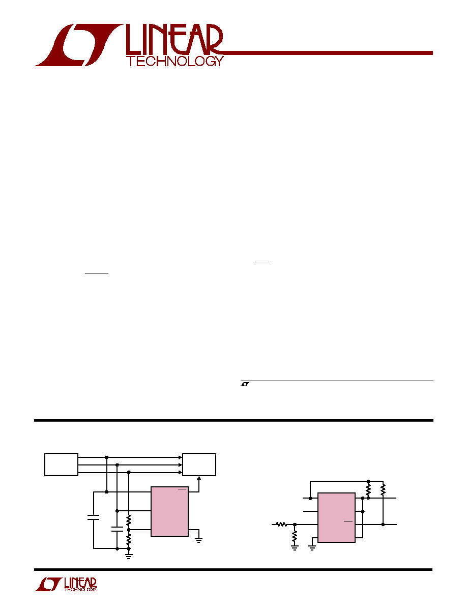
TYPICAL APPLICATIO
U
V
CC3
V
CC5
V
CCA
RST
GND
LTC1728-5
1727/28 TA01
3.3V
5V
1.8V
0.1
µ
F
5
1
2
R1
61.9k
1%
R2
100k
1%
4
3
DC/DC
CONVERTER
SYSTEM
LOGIC
0.1
µ
F
1
2
3
4
8
7
6
5
LTC1727-2.5
R2
1727/28 TA08
R1
ADJUSTABLE
SUPPLY
3.3V
2.5V
R3
10k
POWER
GOOD
SYSTEM
RESET
R4
10k
V
CC3
V
CC25
V
CCA
GND
COMP3
COMP25
RST
COMPA
Triple Supply Monitor with Power Good Output
(3.3V, 2.5V and Adjustable)
2
LTC1727/LTC1728
17278fa
A
U
G
W
A
W
U
W
A
R
BSOLUTE
XI
TI
S
V
CC3
, V
CC5
/V
CC25
/V
CC18
, V
CCA
................... 0.3V to 7V
RST ........................................................... 0.3V to 7V
COMPA, COMP3, COMP25/COMP5
(MS8 and SO-8 Only) ............................ 0.3V to 7V
Operating Temperature Range
(Note 3) ............................................. 40
°
C to 85
°
C
Storage Temperature Range ................ 65
°
C to 150
°
C
Lead Temperature (Soldering, 10 sec)................ 300
°
C
W
U
U
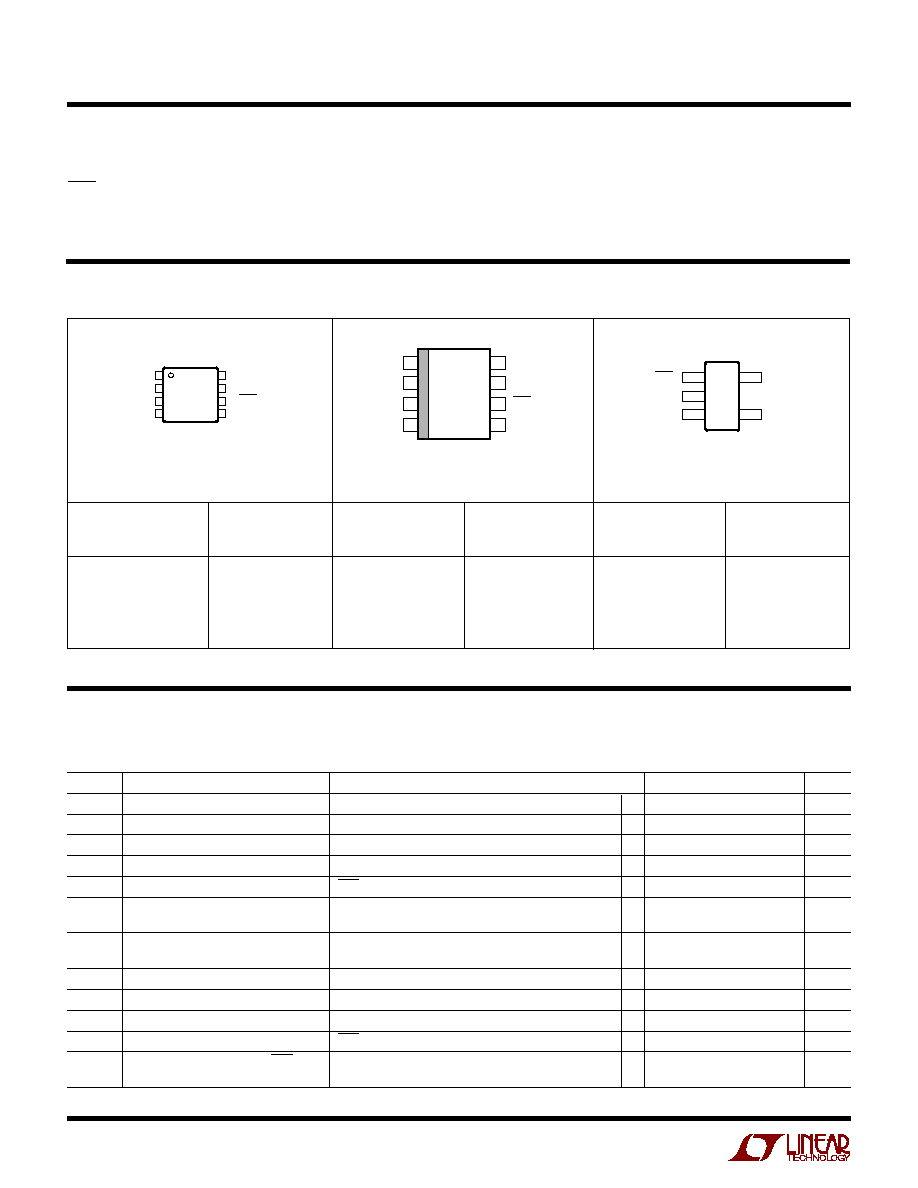
PACKAGE/ORDER I FOR ATIO
ORDER
PART NUMBER
LTC1727EMS8-2.5
LTC1727EMS8-5
MS8
PART MARKING
T
JMAX
= 125
°
C,
JA
= 250
°
C/W
T
JMAX
= 125
°
C,
JA
= 200
°
C/W
(Notes 1, 2)
1
2
3
4
V
CC3
V
CC5
/V
CC25
V
CCA
GND
8
7
6
5
COMP3
COMP25/COMP5
RST
COMPA
TOP VIEW
MS8 PACKAGE
8-LEAD PLASTIC MSOP
RST 1
GND 2
TOP VIEW
S5 PACKAGE
5-LEAD PLASTIC SOT-23
V
CCA
3
5 V
CC3
4
V
CC5
/
V
CC25
/
V
CC18
1
2
3
4
8
7
6
5
TOP VIEW
COMP3
RST
COMPA
V
CC3
V
CCA
GND
S8 PACKAGE
8-LEAD PLASTIC SO
COMP25/
COMP5
V
CC5
/
V
CC25
T
JMAX
= 125
°
C,
JA
= 150
°
C/W
ORDER
PART NUMBER
LTC1727ES8-2.5
LTC1727IS8-2.5
LTC1727ES8-5
LTC1727IS8-5
LTHY
LTHX
S8
PART MARKING
172725
727I25
17275
1727I5
SYMBOL
PARAMETER
CONDITIONS
MIN
TYP
MAX
UNITS
V
RT3
Reset Threshold V
CC3
V
CC3
Input Threshold
q
3.036
3.086
3.135
V
V
RT5
Reset Threshold V
CC5
V
CC5
Input Threshold (5V Version)
q
4.600
4.675
4.750
V
V
RT25
Reset Threshold V
CC25
V
CC25
Input Threshold (2.5V Version)
q
2.300
2.338
2.375
V
V
RTA
Reset Threshold V
CCA
V
CCA
Input Threshold
q
0.985
1.000
1.015
V
V
CCOP
V
CC3
, V
CC5
/V
CC25
Operating Voltage
RST, COMP3, COMP5, COMP25 in Correct Logic State
q
1
7
V
V
CCOPA
V
CC3
, V
CC5
/V
CC25
Operating Voltage
Minimum Supply Voltage to Guarantee COMPA
q
2
2.3
V
in Correct Logic State
I
VCC3
V
CC3
Supply Current
V
CC5
/V
CC25
> V
CC3
q
1
2
µ
A
V
CC5
/V
CC25
< V
CC3
, V
CC3
= 3.3V (Note 4)
q
10
20
µ
A
I
VCC25
V
CC25
Supply Current
V
CC25
< V
CC3
, V
CC25
= 2.5V (Note 4)
q
1
2
µ
A
I
VCC5
V
CC5
Supply Current
V
CC5
= 5V, V
CC3
< V
CC5
q
10
20
µ
A
I
VCCA
V
CCA
Input Current
V
CCA
= 1V
q
15
0
15
nA
t
RST
Reset Pulse Width
RST Low with 10k Pull-Up to V
CC3
(Note 5)
q
140
200
280
ms
t
UV
V
CC
Undervoltage Detect to RST
V
CC5
, V
CC25
, V
CC3
or V
CCA
Less Than Reset
110
µ
s
or COMPX
Threshold V
RT
by More Than 1% (Note 5)
All except LTC1728-1.8/LTC1728-3.3. The
q
denotes specifications which
apply over the full operating temperature range, otherwise specifications are at T
A
= 25
°
C. V
CC3
= 3.3V, V
CC5
= 5V,
V
CC25
= 2.5V, V
CCA
= V
CC3
unless otherwise noted.
ORDER
PART NUMBER
LTC1728ES5-1.8
LTC1728ES5-2.5
LTC1728ES5-3.3
LTC1728ES5-5
S5
PART MARKING
LTPH
LTIA
LTYP
LTHZ
ELECTRICAL CHARACTERISTICS
Consult LTC Marketing for parts specified with wider operating temperature ranges.
3
LTC1727/LTC1728
17278fa
All except LTC1728-1.8/LTC1728-3.3. The
q
denotes specifications which
apply over the full operating temperature range, otherwise specifications are at T
A
= 25
°
C. V
CC3
= 3.3V, V
CC5
= 5V,
V
CC25
= 2.5V, V
CCA
= V
CC3
unless otherwise noted.
SYMBOL
PARAMETER
CONDITIONS
MIN
TYP
MAX
UNITS
V
OL
Output Voltage Low, RST, COMPX
I
SINK
= 2.5mA, V
CC3
= 3V, V
CC5
/V
CC25
= 0V
q
0.15
0.4
V
I
SINK
= 100
µ
A, V
CC3
= 1V, V
CC5
/V
CC25
= 0V
q
0.05
0.3
V
I
SINK
= 100
µ
A, V
CC3
= 0V, V
CC5
/V
CC25
= 1V
q
0.05
0.3
V
I
SINK
= 100
µ
A, V
CC3
= 1V, V
CC5
/V
CC25
= 1V
q
0.05
0.3
V
V
OH
Output Voltage High, RST, COMPX (Note 6)
I
SOURCE
= 1
µ
A
q
V
CC3
1
V
LTC1727-5/LTC1728-5 Only
V
OVR
V
CC5
Reset Override Voltage (Note 7)
Override V
CC5
Ability to Assert RST
V
CC3
±
0.025
V
ELECTRICAL CHARACTERISTICS
SYMBOL
PARAMETER
CONDITIONS
MIN
TYP
MAX
UNITS
V
RT3
Reset Threshold V
CC3
V
CC3
Input Threshold
q
2.760
2.805
2.850
V
V
RT18
Reset Threshold V
CC18
V
CC18
Input Threshold
q
1.656
1.683
1.710
V
V
RTA
Reset Threshold V
CCA
V
CCA
Input Threshold
q
0.985
1.000
1.015
V
V
CCOP
V
CC3
, V
CC18
Operating Voltage
RST in Correct Logic State
q
1
7
V
I
VCC3
V
CC3
Supply Current
V
CC18
> V
CC3
q
1
2
µ
A
V
CC18
< V
CC3
, V
CC3
= 3V (Note 4)
q
10
20
µ
A
I
VCC18
V
CC18
Supply Current
V
CC18
< V
CC3
, V
CC18
= 1.8V (Note 4)
q
1
2
µ
A
I
VCCA
V
CCA
Input Current
V
CCA
= 1V
q
15
0
15
nA
t
RST
Reset Pulse Width
RST Low (Note 5)
q
140
200
280
ms
t
UV
V
CC
Undervoltage Detect to RST
V
CC18
, V
CC3
or V
CCA
Less Than Reset (Note 5)
110
µ
s
Threshold V
RT
by More Than 1%
V
OL
Output Voltage Low, RST
I
SINK
= 2.5mA, V
CC3
= 3V, V
CC18
= 0V
q
0.15
0.4
V
I
SINK
= 100
µ
A, V
CC3
= 1V, V
CC18
= 0V
q
0.05
0.3
V
I
SINK
= 100
µ
A, V
CC3
= 0V, V
CC18
= 1V
q
0.05
0.3
V
I
SINK
= 100
µ
A, V
CC3
= 1V, V
CC18
= 1V
q
0.05
0.3
V
V
OH
Output Voltage High, RST
I
SOURCE
= 1
µ
A (Note 6)
q
V
CC3
1
V
LTC1728-1.8 The
q
denotes specifications which apply over the full operating temperature range, otherwise specifications are at
T
A
= 25
°
C. V
CC3
= 3V, V
CC18
= 1.8V, V
CCA
= V
CC3
unless otherwise noted.
SYMBOL
PARAMETER
CONDITIONS
MIN
TYP
MAX
UNITS
V
RT3
Reset Threshold V
CC3
V
CC3
Input Threshold
q
3.036
3.086
3.135
V
V
RT18
Reset Threshold V
CC18
V
CC18
Input Threshold
q
1.656
1.683
1.710
V
V
RTA
Reset Threshold V
CCA
V
CCA
Input Threshold
q
0.985
1.000
1.015
V
V
CCOP
V
CC3
, V
CC18
Operating Voltage
RST in Correct Logic State
q
1
7
V
I
VCC3
V
CC3
Supply Current
V
CC18
> V
CC3
q
1
2
µ
A
V
CC18
< V
CC3
, V
CC3
= 3.3V (Note 4)
q
10
20
µ
A
I
VCC18
V
CC18
Supply Current
V
CC18
< V
CC3
, V
CC18
= 1.8V (Note 4)
q
1
2
µ
A
I
VCCA
V
CCA
Input Current
V
CCA
= 1V
q
15
0
15
nA
t
RST
Reset Pulse Width
RST Low (Note 5)
q
140
200
280
ms
t
UV
V
CC
Undervoltage Detect to RST
V
CC18
, V
CC3
or V
CCA
Less Than Reset (Note 5)
110
µ
s
Threshold V
RT
by More Than 1%
V
OL
Output Voltage Low, RST
I
SINK
= 2.5mA, V
CC3
= 3.3V, V
CC18
= 0V
q
0.15
0.4
V
I
SINK
= 100
µ
A, V
CC3
= 1V, V
CC18
= 0V
q
0.05
0.3
V
I
SINK
= 100
µ
A, V
CC3
= 0V, V
CC18
= 1V
q
0.05
0.3
V
I
SINK
= 100
µ
A, V
CC3
= 1V, V
CC18
= 1V
q
0.05
0.3
V
V
OH
Output Voltage High, RST
I
SOURCE
= 1
µ
A (Note 6)
q
V
CC3
1
V
LTC1728-3.3 The
q
denotes specifications which apply over the full operating temperature range, otherwise specifications are at
T
A
= 25
°
C. V
CC3
= 3.3V, V
CC18
= 1.8V, V
CCA
= V
CC3
unless otherwise noted.
4
LTC1727/LTC1728
17278fa
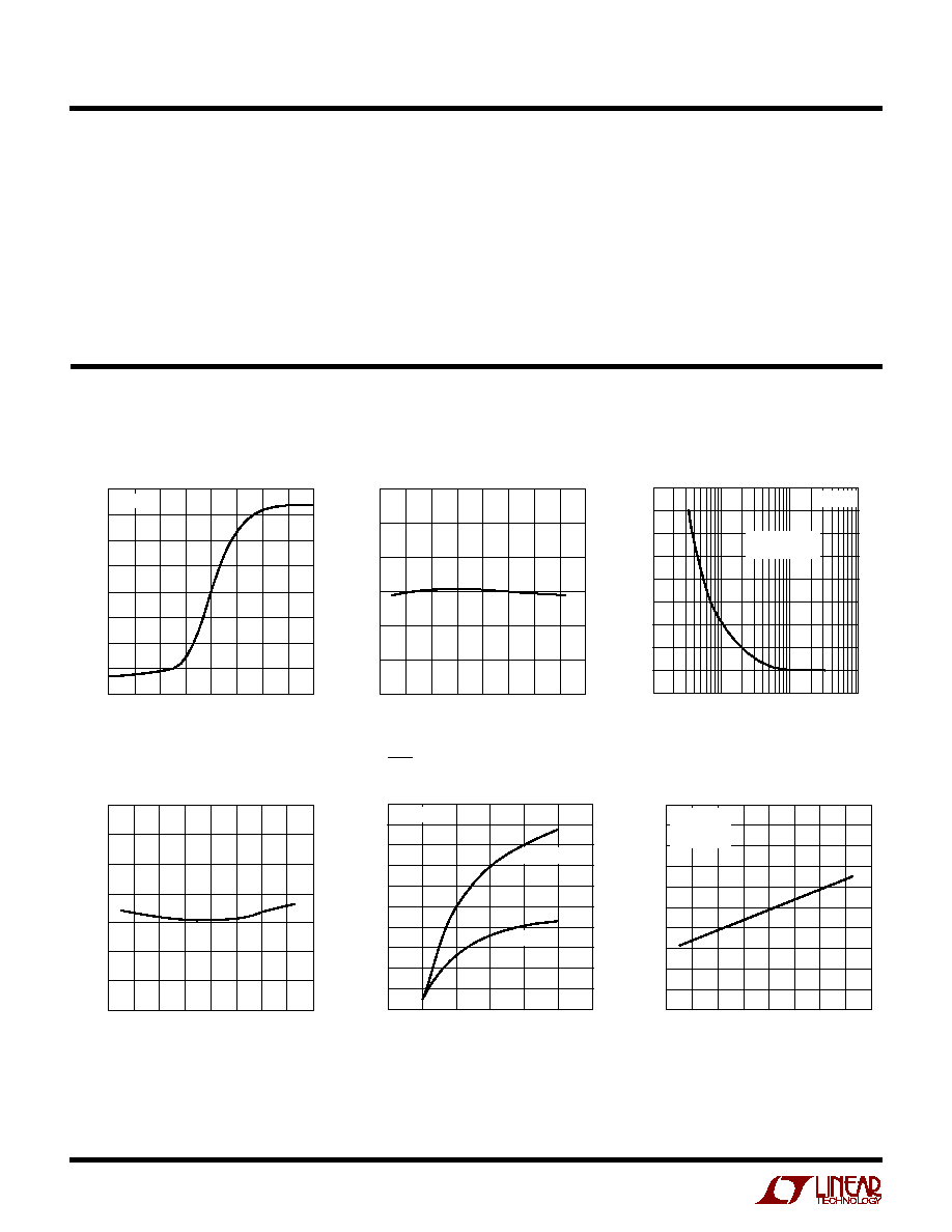
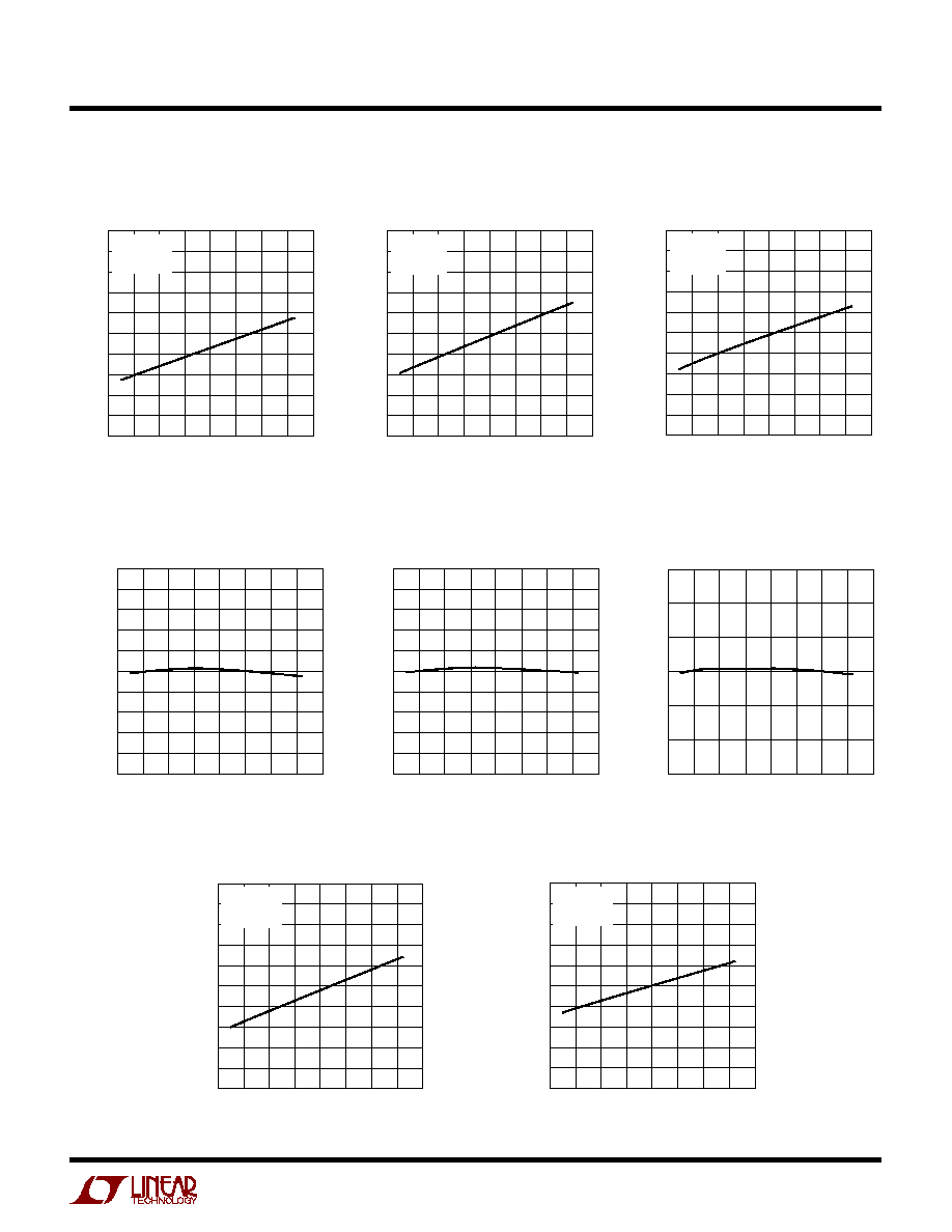
TYPICAL PERFOR A CE CHARACTERISTICS
U
W
V
CCA
Threshold Voltage
vs Temperature
Reset Pulse Width
vs Temperature
Typical Transient Duration
vs Comparator Overdrive
V
CCA
Input Current
vs Input Voltage
INPUT VOLTAGE (V)
0.80 0.85
0.95
1.05
1.15
INPUT CURRENT (nA)
0
1.0
1.20
1727/28 G01
1.0
2.0
0.5
1.5
0.90
1
1.10
2.0
0.5
1.5
T
A
= 25
°
C
TEMPERATURE (
°
C)
60
0.985
V
CCA
THRESHOLD VOLTAGE, V
RTA
(V)
0.990
0.995
1.000
1.005
20
20
60
100
1727/28 G02
1.010
1.015
40
0
40
80
RESET COMPARATOR OVERDRIVE VOLTAGE (% OF V
CC
)
0.1
250
TYPICAL TRANSIENT DIRATION (
µ
s)
300
350
400
450
1
10
100
1727/28 G03
200
150
50
0
100
RESET OCCURS
ABOVE CURVE
T
A
= 25
°
C
I
VCC25
vs Temperature
(LTC1727-2.5/LT1728-2.5)
RST, COMPX I
SINK
vs Supply Voltage
TEMPERATURE (
°
C)
60 40
RESET PULSE WIDTH, t
RST
(ms)
220
240
260
60
1727/28 G04
200
180
20
20
40
80
0
100
160
140
280
V
CC3
OR V
CC5
(V)
0
0
I
SINK
(mA)
2
4
6
1
2
3
4
1727/28 G05
5
8
10
1
3
5
7
9
6
V
OL
= 0.4V
T
A
= 25
°
C
V
OL
= 0.2V
TEMPERATURE (
°
C)
60
0.5
I
VCC25
(
µ
A)
0.6
0.8
0.9
1.0
1.5
1.2
20
20
40
1727/28 G06
0.7
1.3
1.4
1.1
40
0
60
80
100
V
CC3
= 3.3V
V
CC25
= 2.5V
V
CCA
= 3.3V
ELECTRICAL CHARACTERISTICS
Note 5: Measured from when input passes through the input threshold
(V
RTX
) until RST or COMPX passes through 1.5V.
Note 6: The output pins RST and COMPX have internal pull-ups to V
CC3
of
typically 6
µ
A. However, external pull-up resistors may be used when faster
rise times are required or for V
OH
voltages greater than V
CC3
.
Note 7: The V
CC5
reset override voltage is valid for an operating range less
than approximately 4.15V. Above this point the override is turned off and
the V
CC5
pin functions normally.
Note 1: Absolute Maximum Ratings are those values beyond which the life
of the device may be impaired.
Note 2: All voltage values are with respect to GND.
Note 3: The LTC1727E/LTC1728E are guaranteed to meet specified
performance from 0
°
C to 70
°
C and are designed, characterized and
assured to meet the extended temperature limits of 40
°
C to 85
°
C
but are not tested at these temperatures.
Note 4: Both V
CC3
and V
CC5
/V
CC25
/V
CC18
can act as the supply depending
on which pin has the greatest potential.
5
LTC1727/LTC1728
17278fa
TYPICAL PERFOR A CE CHARACTERISTICS
U
W
V
CC25
Threshold Voltage
vs Temperature
(LTC1727-2.5/LTC1728-2.5)
TEMPERATURE (
°
C)
60
V
CC25
THRESHOLD VOLTAGE, V
RT25
(V)
2.3750
2.3675
2.3600
2.3525
2.3450
2.3375
2.3300
2.3225
2.3150
2.3075
2.3000
20
20
40
1727/28 G10
40
0
60
80
100
V
CC5
Threshold Voltage
vs Temperature
(LTC1727-5/LTC1728-5)
V
CC3
Threshold Voltage
vs Temperature
(All But LTC1728-1.8)
TEMPERATURE (
°
C)
60
V
CC3
THRESHOLD VOLTAGE, V
RT3
(V)
3.135
3.125
3.115
3.105
3.095
3.085
3.075
3.065
3.055
3.045
3.035
20
20
40
1727/28 G11
40
0
60
80
100
TEMPERATURE (
°
C)
60
V
CC5
THESHOLD VOLTAGE, V
RT5
(V)
4.675
4.700
4.750
4.725
0
40
100
1727/28 G12
4.650
4.625
4.600
40 20
20
60
80
TEMPERATURE (
°
C)
60
0.5
I
VCC18
(
µ
A)
0.6
0.8
0.9
1.0
1.5
1.2
20
20
40
1727/28 G13
0.7
1.3
1.4
1.1
40
0
60
80
100
V
CC3
= 3V
V
CC18
= 1.8V
V
CCA
= 3V
I
VCC3
vs Temperature
(LTC1728-1.8)
I
VCC18
vs Temperature
(LTC1728-1.8/LTC1728-3.3)
TEMPERATURE (
°
C)
60
5
I
VCC3
(
µ
A)
6
8
9
10
15
12
20
20
40
1727/28 G14
7
13
14
11
40
0
60
80
100
V
CC3
= 3V
V
CC18
= 1.8V
V
CCA
= 3V
I
VCC3
vs Temperature
(LTC1727-5/LTC1728-5)
I
VCC5
vs Temperature
(LTC1727-5/LTC1728-5)
I
VCC3
vs Temperature (LTC1727-2.5/
LTC1728-2.5/LTC1728-3.3)
TEMPERATURE (
°
C)
60
5
I
VCC3
(
µ
A)
6
8
9
10
15
12
20
20
40
1727/28 G07
7
13
14
11
40
0
60
80
100
V
CC3
= 3.3V
V
CC25
= 2.5V
V
CCA
= 3.3V
TEMPERATURE (
°
C)
60
0.5
I
VCC3
(
µ
A)
0.6
0.8
0.9
1.0
1.5
1.2
20
20
40
1727/28 G08
0.7
1.3
1.4
1.1
40
0
60
80
100
V
CC5
= 5V
V
CC3
= 3.3V
V
CCA
= 3.3V
TEMPERATURE (
°
C)
60
5
I
VCC5
(
µ
A)
6
8
9
10
15
12
20
20
40
1727/28 G09
7
13
14
11
40
0
60
80
100
V
CC5
= 5V
V
CC3
= 3.3V
V
CCA
= 3.3V