1
LTC1727/LTC1728
Micropower Precision
Triple Supply Monitors
in 8-Lead MSOP and
5-Lead SOT-23 Packages
s
Monitors Three Inputs Simultaneously
LTC1727-5: 5V, 3.3V and ADJ
LTC1727-2.5: 2.5V, 3.3V and ADJ
LTC1728-5: 5V, 3.3V and ADJ
LTC1728-2.5: 2.5V, 3.3V and ADJ
LTC1728-1.8: 3V, 1.8V and ADJ
s
±
1.5% Threshold Accuracy Over Temperature
s
Very Low Supply Current: 10
µ
A Typ
s
200ms Reset Time Delay
s
Active Low RESET Output
s
Power Supply Glitch Immunity
s
Guaranteed RESET for V
CC3
1V
or V
CC5
/V
CC25
/V
CC18
1V
s
LTC1727 Includes Monitor Output for Each Supply
s
LTC1727: 8-Lead MSOP and SO Packages
s
LTC1728: 5-Lead SOT-23 Package
The LTC
Æ
1727 is a triple supply monitor intended for
systems with multiple supply voltages. Each supply moni-
tor has its own open-drain output for individual supply
monitoring. A common open-drain reset output remains
low until all three supplies have been in compliance for
200ms. Tight 1.5% accuracy specifications and glitch
immunity ensure reliable reset operation without false
triggering.
The LTC1728 is functionally identical to the LTC1727
without the individual monitor outputs.
The RST output is guaranteed to be in the correct state for
V
CC5
/V
CC25
/V
CC18
or V
CC3
down to 1V. The LTC1727/
LTC1728 may also be configured to monitor any one or
two V
CC
inputs instead of three, depending on system
requirements.
Very low (10
µ
A typical) supply current makes the LTC1727/
LTC1728 ideal for power conscious systems.
The LTC1727 is available in an 8-lead MSOP or SO
package and the LTC1728 is available in a 5-lead SOT-23
package.
, LTC and LT are registered trademarks of Linear Technology Corporation.
s
Desktop Computers
s
Notebook Computers
s
Intelligent Instruments
s
Portable Battery-Powered Equipment
s
Network Servers
FEATURES
DESCRIPTIO
U
APPLICATIO S
U
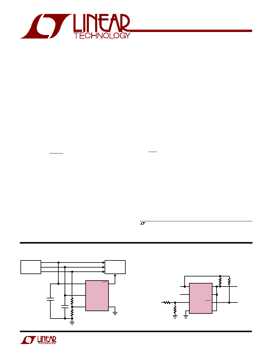
TYPICAL APPLICATIO
U
V
CC3
V
CC5
V
CCA
RST
GND
LTC1728-5
1727/28 TA01
3.3V
5V
1.8V
0.1
µ
F
5
1
2
R1
61.9k
1%
R2
100k
1%
4
3
DC/DC
CONVERTER
SYSTEM
LOGIC
0.1
µ
F
1
2
3
4
8
7
6
5
LTC1727-2.5
R2
1727/28 TA08
R1
ADJUSTABLE
SUPPLY
3.3V
2.5V
R3
10k
POWER
GOOD
SYSTEM
RESET
R4
10k
V
CC3
V
CC25
V
CCA
GND
COMP3
COMP25
RST
COMPA
Triple Supply Monitor with Power Good Output
(3.3V, 2.5V and Adjustable)
2
LTC1727/LTC1728
A
U
G
W
A
W
U
W
A
R
BSOLUTE
XI
TI
S
V
CC3
, V
CC5
/V
CC25
/V
CC18
, V
CCA
................... ≠ 0.3V to 7V
RST ........................................................... ≠ 0.3V to 7V
COMPA, COMP3, COMP25/COMP5
(MS8 and SO-8 Only) ............................ ≠ 0.3V to 7V
Operating Temperature Range
(Note 3) ............................................. ≠ 40
∞
C to 85
∞
C
Storage Temperature Range ................ ≠ 65
∞
C to 150
∞
C
Lead Temperature (Soldering, 10 sec)................ 300
∞
C
W
U
U
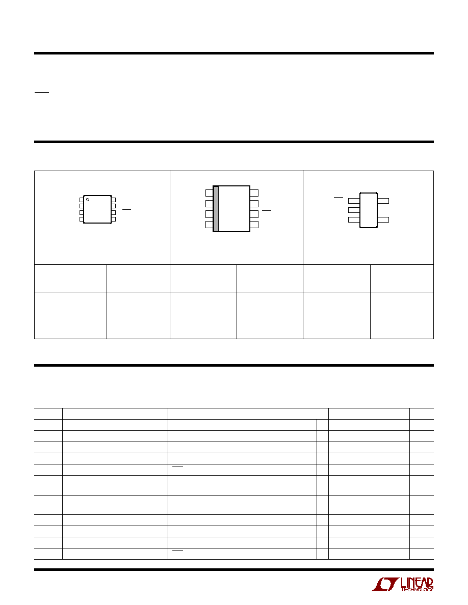
PACKAGE/ORDER I FOR ATIO
ORDER
PART NUMBER
LTC1727EMS8-2.5
LTC1727EMS8-5
MS8
PART MARKING
Consult factory for Military grade parts.
T
JMAX
= 125
∞
C,
JA
= 250
∞
C/W
T
JMAX
= 125
∞
C,
JA
= 200
∞
C/W
(Notes 1, 2)
1
2
3
4
V
CC3
V
CC5
/V
CC25
V
CCA
GND
8
7
6
5
COMP3
COMP25/COMP5
RST
COMPA
TOP VIEW
MS8 PACKAGE
8-LEAD PLASTIC MSOP
RST 1
GND 2
TOP VIEW
S5 PACKAGE
5-LEAD PLASTIC SOT-23
V
CCA
3
5 V
CC3
4
V
CC5
/
V
CC25
/
V
CC18
1
2
3
4
8
7
6
5
TOP VIEW
COMP3
RST
COMPA
V
CC3
V
CCA
GND
S8 PACKAGE
8-LEAD PLASTIC SO
COMP25/
COMP5
V
CC5
/
V
CC25
T
JMAX
= 125
∞
C,
JA
= 150
∞
C/W
ORDER
PART NUMBER
LTC1727ES8-2.5
LTC1727IS8-2.5
LTC1727ES8-5
LTC1727IS8-5
LTHY
LTHX
S8
PART MARKING
172725
727I25
17275
1727I5
SYMBOL
PARAMETER
CONDITIONS
MIN
TYP
MAX
UNITS
V
RT3
Reset Threshold V
CC3
V
CC3
Input Threshold
q
3.036
3.086
3.135
V
V
RT5
Reset Threshold V
CC5
V
CC5
Input Threshold (5V Version)
q
4.600
4.675
4.750
V
V
RT25
Reset Threshold V
CC25
V
CC25
Input Threshold (2.5V Version)
q
2.300
2.338
2.375
V
V
RTA
Reset Threshold V
CCA
V
CCA
Input Threshold
q
0.985
1.000
1.015
V
V
CCOP
V
CC3
, V
CC5
/V
CC25
Operating Voltage
RST, COMP3, COMP5, COMP25 in Correct Logic State
q
1
7
V
V
CCOPA
V
CC3
, V
CC5
/V
CC25
Operating Voltage
Minimum Supply Voltage to Guarantee COMPA
q
2
2.3
V
in Correct Logic State
I
VCC3
V
CC3
Supply Current
V
CC5
/V
CC25
> V
CC3
q
1
2
µ
A
V
CC5
/V
CC25
< V
CC3
, V
CC3
= 3.3V (Note 4)
q
10
20
µ
A
I
VCC25
V
CC25
Supply Current
V
CC25
< V
CC3
, V
CC25
= 2.5V (Note 4)
q
1
2
µ
A
I
VCC5
V
CC5
Supply Current
V
CC5
= 5V, V
CC3
< V
CC5
q
10
20
µ
A
I
VCCA
V
CCA
Input Current
V
CCA
= 1V
q
≠ 15
0
15
nA
t
RST
Reset Pulse Width
RST Low with 10k Pull-Up to V
CC3
(Note 5)
q
140
200
280
ms
All except LTC1728-1.8. The
q
denotes specifications which apply over the
full operating temperature range, otherwise specifications are at T
A
= 25
∞
C. V
CC3
= 3.3V, V
CC5
= 5V, V
CC25
= 2.5V, V
CCA
= V
CC3
unless
otherwise noted.
ORDER
PART NUMBER
LTC1728ES5-1.8
LTC1728ES5-2.5
LTC1728ES5-5
S5
PART MARKING
LTPH
LTIA
LTHZ
ELECTRICAL CHARACTERISTICS
3
LTC1727/LTC1728
Note 5: Measured from when input passes through the input threshold
(V
RTX
) until RST or COMPX passes through 1.5V.
Note 6: The output pins RST and COMPX have internal pull-ups to V
CC3
of
typically 6
µ
A. However, external pull-up resistors may be used when faster
rise times are required or for V
OH
voltages greater than V
CC3
.
Note 7: The V
CC5
reset override voltage is valid for an operating range less
than approximately 4.15V. Above this point the override is turned off and
the V
CC5
pin functions normally.
Note 1: Absolute Maximum Ratings are those values beyond which the life
of the device may be impaired.
Note 2: All voltage values are with respect to GND.
Note 3: The LTC1727E/LTC1728E are guaranteed to meet specified
performance from 0
∞
C to 70
∞
C and are designed, characterized and
assured to meet the extended temperature limits of ≠ 40
∞
C to 85
∞
C
but are not tested at these temperatures.
Note 4: Both V
CC3
and V
CC5
/V
CC25
/V
CC18
can act as the supply depending
on which pin has the greatest potential.
All except LTC1728-1.8. The
q
denotes specifications which apply over the
full operating temperature range, otherwise specifications are at T
A
= 25
∞
C. V
CC3
= 3.3V, V
CC5
= 5V, V
CC25
= 2.5V, V
CCA
= V
CC3
unless
otherwise noted.
SYMBOL
PARAMETER
CONDITIONS
MIN
TYP
MAX
UNITS
t
UV
V
CC
Undervoltage Detect to RST
V
CC5
, V
CC25
, V
CC3
or V
CCA
Less Than Reset
110
µ
s
or COMPX
Threshold V
RT
by More Than 1% (Note 5)
V
OL
Output Voltage Low, RST, COMPX
I
SINK
= 2.5mA, V
CC3
= 3V, V
CC5
/V
CC25
= 0V
q
0.15
0.4
V
I
SINK
= 100
µ
A, V
CC3
= 1V, V
CC5
/V
CC25
= 0V
q
0.05
0.3
V
I
SINK
= 100
µ
A, V
CC3
= 0V, V
CC5
/V
CC25
= 1V
q
0.05
0.3
V
I
SINK
= 100
µ
A, V
CC3
= 1V, V
CC5
/V
CC25
= 1V
q
0.05
0.3
V
V
OH
Output Voltage High, RST, COMPX (Note 6)
I
SOURCE
= 1
µ
A
q
V
CC3
≠ 1
V
LTC1727-5/LTC1728-5 Only
V
OVR
V
CC5
Reset Override Voltage (Note 7)
Override V
CC5
Ability to Assert RST
V
CC3
±
0.025
V
ELECTRICAL CHARACTERISTICS
SYMBOL
PARAMETER
CONDITIONS
MIN
TYP
MAX
UNITS
V
RT3
Reset Threshold V
CC3
V
CC3
Input Threshold
q
2.760
2.805
2.850
V
V
RT18
Reset Threshold V
CC18
V
CC18
Input Threshold
q
1.656
1.683
1.710
V
V
RTA
Reset Threshold V
CCA
V
CCA
Input Threshold
q
0.985
1.000
1.015
V
V
CCOP
V
CC3
, V
CC18
Operating Voltage
RST in Correct Logic State
q
1
7
V
I
VCC3
V
CC3
Supply Current
V
CC18
> V
CC3
q
1
2
µ
A
V
CC18
< V
CC3
, V
CC3
= 3V (Note 4)
q
10
20
µ
A
I
VCC18
V
CC18
Supply Current
V
CC18
< V
CC3
, V
CC18
= 1.8V (Note 4)
q
1
2
µ
A
I
VCCA
V
CCA
Input Current
V
CCA
= 1V
q
≠ 15
0
15
nA
t
RST
Reset Pulse Width
RST Low (Note 5)
q
140
200
280
ms
t
UV
V
CC
Undervoltage Detect to RST
V
CC18
, V
CC3
or V
CCA
Less Than Reset (Note 5)
110
µ
s
Threshold V
RT
by More Than 1%
V
OL
Output Voltage Low, RST
I
SINK
= 2.5mA, V
CC3
= 3V, V
CC18
= 0V
q
0.15
0.4
V
I
SINK
= 100
µ
A, V
CC3
= 1V, V
CC18
= 0V
q
0.05
0.3
V
I
SINK
= 100
µ
A, V
CC3
= 0V, V
CC18
= 1V
q
0.05
0.3
V
I
SINK
= 100
µ
A, V
CC3
= 1V, V
CC18
= 1V
q
0.05
0.3
V
V
OH
Output Voltage High, RST
I
SOURCE
= 1
µ
A (Note 6)
q
V
CC3
≠ 1
V
LTC1728-1.8 The
q
denotes specifications which apply over the full operating temperature range, otherwise specifications are at
T
A
= 25
∞
C. V
CC3
= 3V, V
CC18
= 1.8V, V
CCA
= V
CC3
unless otherwise noted.
4
LTC1727/LTC1728
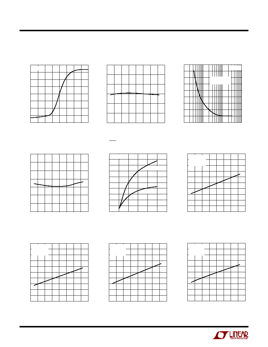
TYPICAL PERFOR A CE CHARACTERISTICS
U
W
V
CCA
Threshold Voltage
vs Temperature
Reset Pulse Width
vs Temperature
Typical Transient Duration
vs Comparator Overdrive
V
CCA
Input Current
vs Input Voltage
INPUT VOLTAGE (V)
0.80 0.85
0.95
1.05
1.15
INPUT CURRENT (nA)
0
1.0
1.20
1727/28 G01
≠1.0
≠ 2.0
≠ 0.5
≠1.5
0.90
1
1.10
2.0
0.5
1.5
T
A
= 25
∞
C
TEMPERATURE (
∞
C)
≠60
0.985
V
CCA
THRESHOLD VOLTAGE, V
RTA
(V)
0.990
0.995
1.000
1.005
≠20
20
60
100
1727/28 G02
1.010
1.015
≠40
0
40
80
RESET COMPARATOR OVERDRIVE VOLTAGE (% OF V
CC
)
0.1
250
TYPICAL TRANSIENT DIRATION (
µ
s)
300
350
400
450
1
10
100
1727/28 G03
200
150
50
0
100
RESET OCCURS
ABOVE CURVE
T
A
= 25
∞
C
I
VCC25
vs Temperature
(LTC1727-2.5/LT1728-2.5)
RST, COMPX I
SINK
vs Supply Voltage
TEMPERATURE (
∞
C)
≠60 ≠40
RESET PULSE WIDTH, t
RST
(ms)
220
240
260
60
1727/28 G04
200
180
≠20
20
40
80
0
100
160
140
280
V
CC3
OR V
CC5
(V)
0
0
I
SINK
(mA)
2
4
6
1
2
3
4
1727/28 G05
5
8
10
1
3
5
7
9
6
V
OL
= 0.4V
T
A
= 25
∞
C
V
OL
= 0.2V
TEMPERATURE (
∞
C)
≠ 60
0.5
I
VCC25
(
µ
A)
0.6
0.8
0.9
1.0
1.5
1.2
≠ 20
20
40
1727/28 G06
0.7
1.3
1.4
1.1
≠40
0
60
80
100
V
CC3
= 3.3V
V
CC25
= 2.5V
V
CCA
= 3.3V
I
VCC3
vs Temperature
(LTC1727-5/LTC1728-5)
I
VCC5
vs Temperature
(LTC1727-5/LTC1728-5)
I
VCC3
vs Temperature
(LTC1727-2.5/LT1728-2.5)
TEMPERATURE (
∞
C)
≠ 60
5
I
VCC3
(
µ
A)
6
8
9
10
15
12
≠ 20
20
40
1727/28 G07
7
13
14
11
≠40
0
60
80
100
V
CC3
= 3.3V
V
CC25
= 2.5V
V
CCA
= 3.3V
TEMPERATURE (
∞
C)
≠ 60
0.5
I
VCC3
(
µ
A)
0.6
0.8
0.9
1.0
1.5
1.2
≠ 20
20
40
1727/28 G08
0.7
1.3
1.4
1.1
≠40
0
60
80
100
V
CC5
= 5V
V
CC3
= 3.3V
V
CCA
= 3.3V
TEMPERATURE (
∞
C)
≠ 60
5
I
VCC5
(
µ
A)
6
8
9
10
15
12
≠ 20
20
40
1727/28 G09
7
13
14
11
≠40
0
60
80
100
V
CC5
= 5V
V
CC3
= 3.3V
V
CCA
= 3.3V
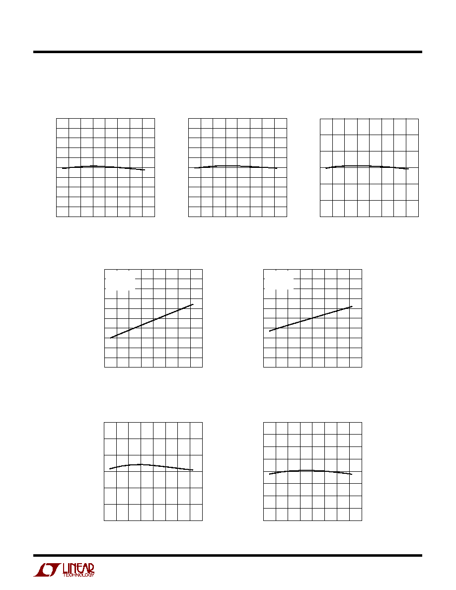
5
LTC1727/LTC1728
TYPICAL PERFOR A CE CHARACTERISTICS
U
W
V
CC25
Threshold Voltage
vs Temperature
(LTC1727-2.5/LTC1728-2.5)
TEMPERATURE (
∞
C)
≠ 60
V
CC25
THRESHOLD VOLTAGE, V
RT25
(V)
2.3750
2.3675
2.3600
2.3525
2.3450
2.3375
2.3300
2.3225
2.3150
2.3075
2.3000
≠ 20
20
40
1727/28 G10
≠40
0
60
80
100
V
CC5
Threshold Voltage
vs Temperature
(LTC1727-5/LTC1728-5)
V
CC3
Threshold Voltage
vs Temperature
(All But LTC1728-1.8)
TEMPERATURE (
∞
C)
≠ 60
V
CC3
THRESHOLD VOLTAGE, V
RT3
(V)
3.135
3.125
3.115
3.105
3.095
3.085
3.075
3.065
3.055
3.045
3.035
≠ 20
20
40
1727/28 G11
≠40
0
60
80
100
TEMPERATURE (
∞
C)
≠60
V
CC5
THESHOLD VOLTAGE, V
RT5
(V)
4.675
4.700
4.750
4.725
0
40
100
1727/28 G12
4.650
4.625
4.600
≠40 ≠20
20
60
80
TEMPERATURE (
∞
C)
≠ 60
0.5
I
VCC18
(
µ
A)
0.6
0.8
0.9
1.0
1.5
1.2
≠ 20
20
40
1727/28 G13
0.7
1.3
1.4
1.1
≠40
0
60
80
100
V
CC3
= 3V
V
CC18
= 1.8V
V
CCA
= 3V
V
CC3
Threshold Voltage
vs Temperature (LTC1728-1.8)
V
CC18
Threshold Voltage
vs Temperature (LTC1728-1.8)
I
VCC3
vs Temperature
(LTC1728-1.8)
I
VCC18
vs Temperature
(LTC1728-1.8)
TEMPERATURE (
∞
C)
≠ 60
5
I
VCC3
(
µ
A)
6
8
9
10
15
12
≠ 20
20
40
1727/28 G14
7
13
14
11
≠40
0
60
80
100
V
CC3
= 3V
V
CC18
= 1.8V
V
CCA
= 3V
TEMPERATURE (
∞
C)
≠60
1.650
V
CC18
THRESHOLD VOLTAGE, V
RT18
(V)
1.660
1.670
1.680
1.690
≠20
20
60
100
1727/28 G15
1.700
1.710
≠40
0
40
80
TEMPERATURE (
∞
C)
≠ 60
V
CC3
THRESHOLD VOLTAGE, V
RT3
(V)
2.845
2.835
2.825
2.815
2.805
2.795
2.785
2.775
2.765
≠ 20
20
40
1727/28 G16
≠40
0
60
80
100

6
LTC1727/LTC1728
(LTC1727/LTC1728)
U
U
U
PI FU CTIO S
V
CC3
(Pin 1/Pin 5): 3.3V Sense Input and Power
Supply Pin. (3V Sense Input and Power Supply Pin for
LTC1728-1.8.) This pin provides power to the part
when the voltage on V
CC3
is greater than the voltage on
V
CC5
/V
CC25
/V
CC18
. Bypass to ground with a
0.1
µ
F
ceramic capacitor.
V
CC5
(Pin 2/Pin 4): 5V Sense Input and Power Supply
Pin. This pin is used on the LTC1727-5/LTC1728-5 to
provide power to the part when the voltage on V
CC5
is
greater than the voltage on V
CC3
. Bypass to ground with
a
0.1
µ
F ceramic capacitor.
V
CC25
(Pin 2/Pin 4): 2.5V Sense Input and Power Supply
Pin. This pin is used on the LTC1727-2.5/LTC1728-2.5 to
provide power to the part when the voltage on V
CC25
is
greater than the voltage on V
CC3
. Bypass to ground with
a
0.1
µ
F ceramic capacitor.
V
CC18
(Pin 2/Pin 4): 1.8V Sense Input and Power Supply
Pin. This pin is used on the LTC1728-1.8 to provide
power to the part when the voltage on V
CC18
is greater
than the voltage on V
CC3
. Bypass to ground with a
0.1
µ
F
ceramic capacitor.
V
CCA
(Pin 3/Pin 3): 1V Sense, High Impedance Input. If
unused, it can be tied to either V
CC3
or V
CC5
/V
CC25
/V
CC18
.
GND (Pin 4/Pin 2): Ground.
COMPA (Pin 5): V
CCA
Comparator Output for the LTC1727.
Active high, open-drain logic output with weak pull-up to
V
CC3
. Asserted when V
CCA
is above V
RTA
. Deasserted
when V
CCA
is below V
RTA
or if both the V
CC3
and V
CC5
supply pins are too low to power the internal bandgap
reference (typically < 2.0V). Can be pulled greater than
V
CC3
using an external pull-up.
RST (Pin 6/Pin 1): Reset Logic Output. Active low, open-
drain logic output with weak pull-up to V
CC3
. Can be pulled
up greater than V
CC3
when interfacing to 5V logic. As-
serted when one or all of the supplies are below trip thresh-
olds and held for 200ms after all supplies become valid.
COMP5 (Pin 7): V
CC5
Comparator Output for the
LTC1727-5. Active high, open-drain logic output with
weak pull-up to V
CC3
. Asserted when V
CC5
is above V
RT5
.
Can be pulled greater than V
CC3
using an external pull-up.
COMP25 (Pin 7): V
CC25
Comparator Output for the
LTC1727-2.5. Active high, open-drain logic output with
weak pull-up to V
CC3
. Asserted when V
CC25
is above
V
RT25
. Can be pulled greater than V
CC3
using an external
pull-up.
COMP3 (Pin 8): V
CC3
Comparator Output for the LTC1727.
Active high, open-drain logic output with weak pull-up to
V
CC3
. Asserted when V
CC3
is above V
RT3
. Can be pulled
greater than V
CC3
using an external pull-up.
7
LTC1727/LTC1728
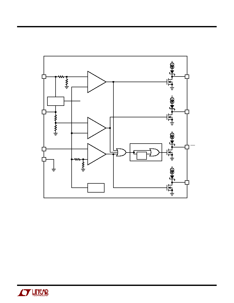
BLOCK DIAGRA S
W
LTC1727-5/LTC1727-2.5
200ms
DELAY
V
CC
INTERNAL
BANDGAP
REFERENCE
POWER
DETECT
200ms PULSE GENERATOR
≠
+
≠
+
≠
+
1
V
CC3
2
V
CC5
/
V
CC25
3
V
CCA
4
GND
5
COMPA
1727 BD1
6
RST
7
COMP25/
COMP5
8
COMP3
6
µ
A
V
CC3
6
µ
A
V
CC3
6
µ
A
V
CC3
6
µ
A
V
CC3
8
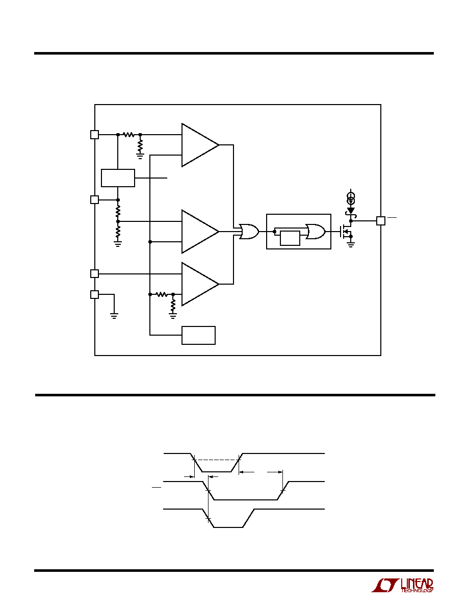
LTC1727/LTC1728
BLOCK DIAGRA S
W
LTC1728-5/LTC1728-2.5/LTC1728-1.8
V
CC
Monitor Timing
TI I G DIAGRA
U
W
W
t
RST
t
UV
1.5V
1727 TD01
V
RTX
V
CCX
RST
COMPX
200ms
DELAY
V
CC
INTERNAL
BANDGAP
REFERENCE
POWER
DETECT
200ms PULSE GENERATOR
≠
+
≠
+
≠
+
5
V
CC3
4
V
CC5
/
V
CC25
/
V
CC18
3
V
CCA
2
GND
1727 BD2
1
RST
6
µ
A
V
CC3
9
LTC1727/LTC1728
Power-Down
On power-down, once any of the V
CC
inputs drop below
its threshold, RST is held at a logic low. A logic low of 0.3V
is guaranteed until both V
CC3
and V
CC5
/V
CC25
/V
CC18
drop
below 1V.
Glitch Immunity
The RST output of the LTC1727/LTC1728 have two forms
of glitch immunity built in. First, the input monitors require
the input voltage to transition at least 10% of the input
threshold (0.1 ∑ V
RTH
) below the input threshold for
approximately 50
µ
s in order to force the monitor output
low. The duration of the transition must be longer for
voltage transitions of lesser magnitude (see Figure 1).
Secondly, the reset pulse width of approximately 200ms
acts to debounce the RST output ensuring that the RST
output will always be in the correct state.
The individual monitor outputs of the LTC1727 do not
have hysteresis and will track the monitor inputs relative
to the monitor's input threshold (V
RTA
, V
RT25
, V
RT3
and
V
RT5
). A very slow moving input voltage with ripple riding
on it may cause the individual monitor outputs (COMPA,
COMP25, COMP3 and COMP5) to toggle on the ripple as
the input voltage passes the input threshold. The slow
response time of the LTC1727's input monitors has a
tendency to integrate signals on the inputs improving their
immunity to noise and ripple.
APPLICATIO S I FOR ATIO
W
U
U
U
Supply Monitoring
The LTC1727 is a low power, high accuracy triple supply
monitoring circuit with three monitor outputs and a
200ms microprocessor reset output.
The LTC1728 is a low power, high accuracy triple supply
monitoring circuit with a single 200ms microprocessor
reset output.
All three V
CC
inputs must be above predetermined thresh-
olds for reset not to be invoked. The LTC1727/LTC1728
will assert reset during power-up, power-down and brown-
out conditions on any one or all of the V
CC
inputs.
Power Detect
The LTC1727/LTC1728 are powered from the 3.3V/3V
input pin (V
CC3
), the 1.8V input pin (V
CC18
), the 2.5V
input pin (V
CC25
) or the 5V input pin (V
CC5
), whichever
pin has the highest potential. This ensures the part pulls
the RST pin low as soon as either input pin is
1V.
Power-Up
Upon power-up, either the V
CC5
/V
CC25
/V
CC18
or V
CC3
pin,
can power the part. This ensures that RST will be low when
either V
CC5
/V
CC25
/V
CC18
or V
CC3
reaches 1V. As long as
any one of the V
CC
inputs is below its predetermined
threshold, RST will stay a logic low. Once all of the V
CC
inputs rise above their thresholds, an internal timer is
started and RST is released after 200ms.
RST is reasserted whenever any one of the V
CC
inputs
drops below its predetermined threshold and remains
asserted until 200ms after all of the V
CC
inputs are above
their thresholds.
On the LTC1727, each of the comparator outputs will be
low until the V
CC
input that is monitored by that compara-
tor rises above the appropriate predetermined threshold.
The COMP3, and COMP5/COMP25 outputs are guaran-
teed to be in the correct logic state for either V
CC3
or
V
CC5
/V
CC25
greater than 1V. The COMPA output requires
the internal bandgap reference to be valid before the
correct logic state can be output. Therefore, the COMPA
output will be held low until V
CCA
is above 1V and V
CC3
or
V
CC5
/V
CC25
is greater than 2V (typ).
RESET MONITOR OVERDRIVE VOLTAGE (% OF V
CC
)
0.1
250
TRANSIENT DURATION (
µ
s)
300
350
400
450
1
10
100
1727/28 F01
200
150
50
0
100
Figure 1. Transient Duration vs Comparator Overdrive
10
LTC1727/LTC1728
Override Functions (5V Versions Only)
The V
CCA
pin, if unused, can be tied to either V
CC3
or V
CC5
.
This is an obvious solution since the trip points for V
CC3
and V
CC5
will always be greater than the trip point for V
CCA
.
The V
CC5
input trip point is disabled if its voltage is equal
to the voltage on V
CC3
±
25mV and the voltage on V
CC5
is
less than 4.15V. In this manner, the LTC1727-5/
LTC1728-5 will behave as a 3.3V monitor and V
CC5
reset
capability will be disabled.
The V
CC5
trip point is reenabled when the voltage on V
CC5
is equal to the voltage on V
CC3
±
25mV and the two inputs
are greater than approximately 4.15V. In this manner, the
part can function as a 5V monitor with the 3.3V monitor
disabled.
APPLICATIO S I FOR ATIO
W
U
U
U
Figure 3. RST Voltage vs Supply Voltage
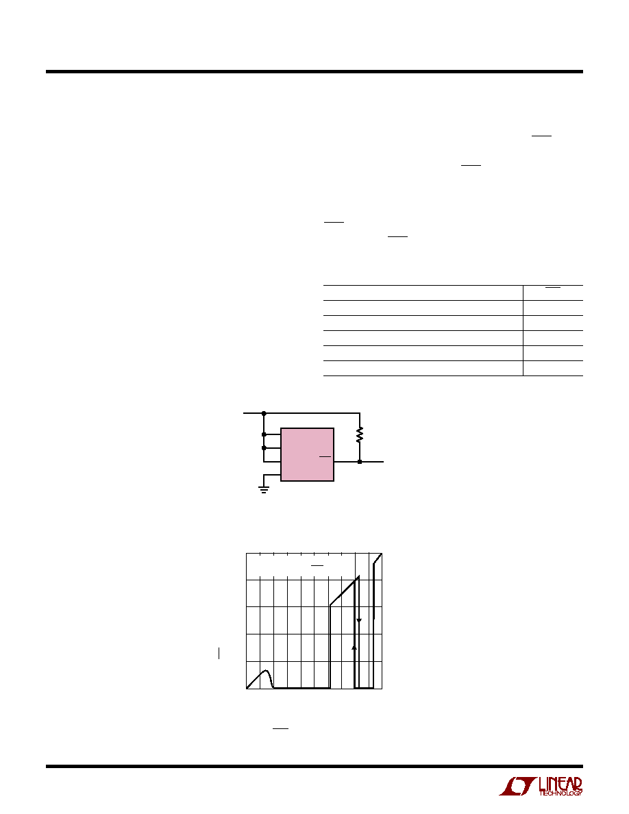
Figure 2. Single Supply Monitor with Others Disabled
When monitoring either 3.3V or 5V with V
CC3
strapped to
V
CC5
(see Figure 2), the part determines which is the
appropriate range. The part handles this situation as
shown in Figure 3. Above 1V and below V
RT3
, RST is held
low. From V
RT3
to approximately 4.15V the part assumes
3.3V supply monitoring and RST is deasserted. Above
approximately 4.15V the part operates as a 5V monitor.
In most systems the 5V supply will pass through the 3.1V
to 4.15V region in < 200ms during power-up, and the
RST output will behave as desired. Table 1 summarizes
the state of RST at various operating voltages with
V
CC3
= V
CC5
.
Table 1. Override Truth Table (V
CC3
= V
CC5
)
INPUTS (V
CC3
= V
CC5
= V
CC
)
RST
0V
V
CC
1V
--
1V
V
CC
V
RT3
0
V
RT3
V
CC
4.15V
1
4.15V
V
CC
V
RT5
0
V
RT5
V
CC
1
V
CC3
V
CC5
V
CCA
GND
1
5
4
3
2
RST
LTC1728-5
1727/28 F02
TO SYSTEM
RESET
R1
10k
V
CC
3.3V OR 5V
SUPPLY VOLTAGE (V)
0
RST OUTPUT VOLTAGE (V)
3
4
5
4
1727/28 F03
2
1
0
1
2
3
5
V
CC3
= V
CC5
= V
CCA
= 0V TO 5V
10k PULL-UP FROM RST TO V
CC3
11
LTC1727/LTC1728
APPLICATIO S I FOR ATIO
W
U
U
U
Figure 5. RST Output Voltage
Characteristics of the Circuit in Figure 4
V
CC5
(V)
0
0.5 1.0 1.5 2.0 2.5 3.0 3.5 4.0 4.5 5.0
RST OUTPUT VOLTAGE (V)
1727/28 F05
5
4
3
2
1
0
V
CC5
= V
CCA
= 0V TO 5V
10k PULL-UP FROM RST TO V
CC5
T
A
= 25
∞
C
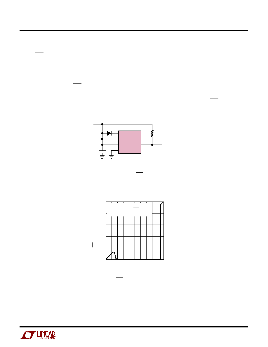
Figure 4 contains a simple circuit for 5V systems that can't
risk the RST output going high in the 3.1V to 4.15V range
(possibly due to very slow rise time on the 5V supply).
Diode D1 powers the LTC1728-5 while dropping
0.6V
from the V
CC5
pin to the V
CC3
pin. This prevents the part's
internal override circuit from being activated. Without the
override circuit active, the RST pin stays low until V
CC5
reaches V
RT5
4.675V. (See Figure 5.)
Figure 4. LTC1728-5 Monitoring a Single 5V
Supply. D1 Used to Avoid RST High Near 3.1V
to 4V (See Figure 3).
V
CC3
V
CC5
V
CCA
GND
1
5
4
3
2
RST
LTC1728-5
1727/28 F04
TO SYSTEM
RESET
R1
10k
5V
0.1
µ
F
D1
D1: MMBD914 OR EQUIVALENT
LTC1727-2.5/LTC1728-2.5/LTC1728-1.8
Override Functions
The V
CCA
pin, if unused, can be tied to either V
CC3
or V
CC25
/
V
CC18
. This is an obvious solution since the trip points for
V
CC3
and V
CC25
/V
CC18
will always be greater than the trip
point for V
CCA
. Likewise, the V
CC25
/V
CC18
, if unused, can
be tied to V
CC3
. V
CC3
must always be used. Tying V
CC3
to
V
CC25
/V
CC18
and operating off of a 2.5V/1.8V supply will
result in the continuous assertion of RST.
12
LTC1727/LTC1728
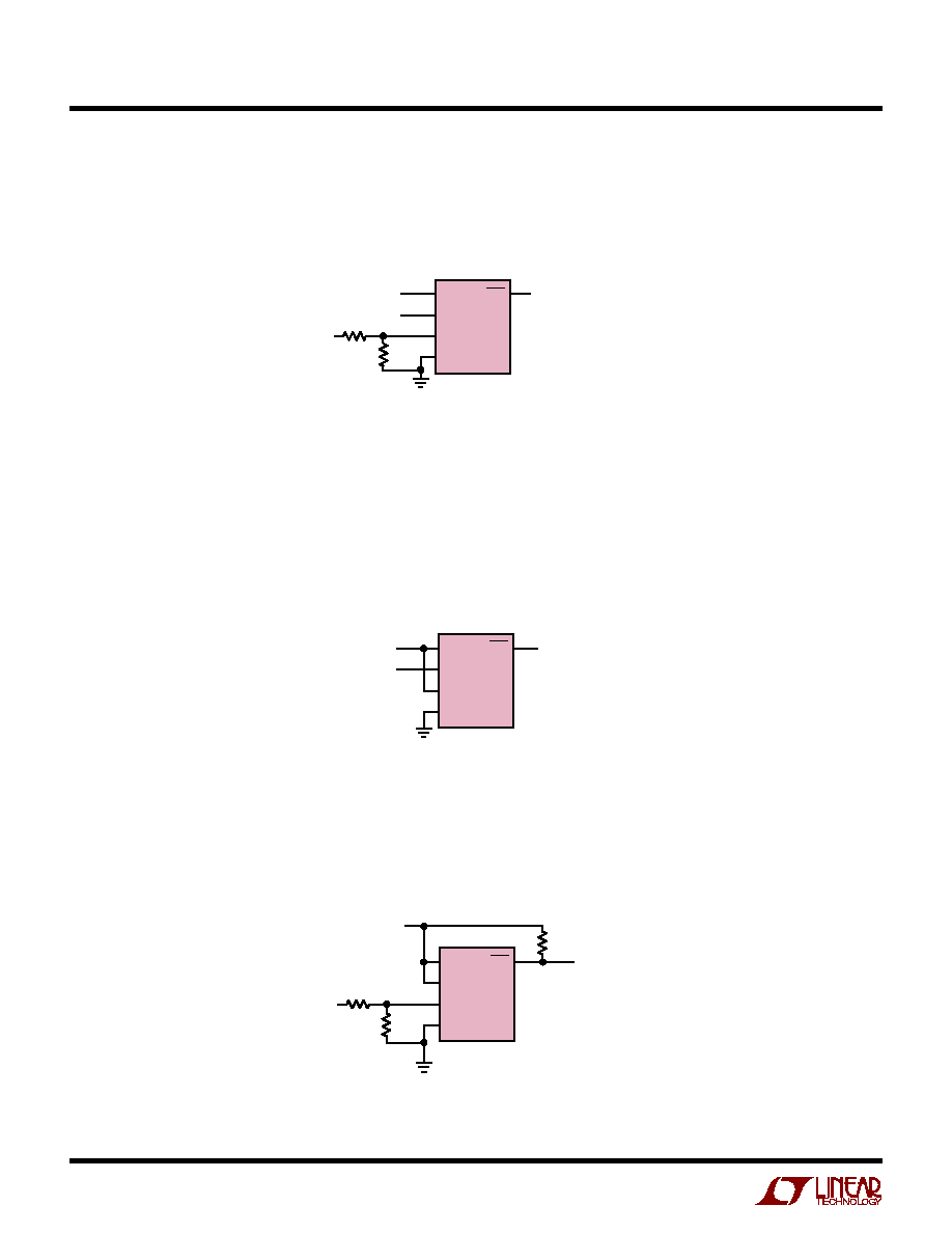
TYPICAL APPLICATIO S
U
Triple Supply Monitor (3.3V, 5V and Adjustable)
5
4
3
2
1
V
CC3
V
CC5
V
CCA
GND
RST
LTC1728-5
3.3V
SYSTEM RESET
*TO PRESERVE THRESHOLD ACCURACY, SET PARALLEL
COMBINATION OF R1 AND R2
66.5k
5V
R2*
R1*
1727/28 TA03
ADJUSTABLE SUPPLY
OR DC/DC FEEDBACK
DIVIDER
Dual Supply Monitor (3.3V and 5V, Defeat V
CCA
Input)
5
4
3
2
1
V
CC3
V
CC5
V
CCA
GND
RST
LTC1728-5
3.3V
SYSTEM RESET
5V
1727/28 TA04
Dual Supply Monitor (3.3V or 5V Plus Adjustable)
5
4
3
2
1
V
CC3
V
CC5
V
CCA
GND
RST
LTC1728-5
R2*
1727/28 TA05
R1*
ADJUSTABLE
SUPPLY
3.3V OR
5V
10k
SYSTEM RESET
*TO PRESERVE THRESHOLD ACCURACY, SET PARALLEL
COMBINATION OF R1 AND R2
66.5k
REFER TO LTC1728-5 OVERRIDE FUNCTIONS IN
THE APPLICATIONS INFORMATION SECTION
13
LTC1727/LTC1728
TYPICAL APPLICATIO S
U
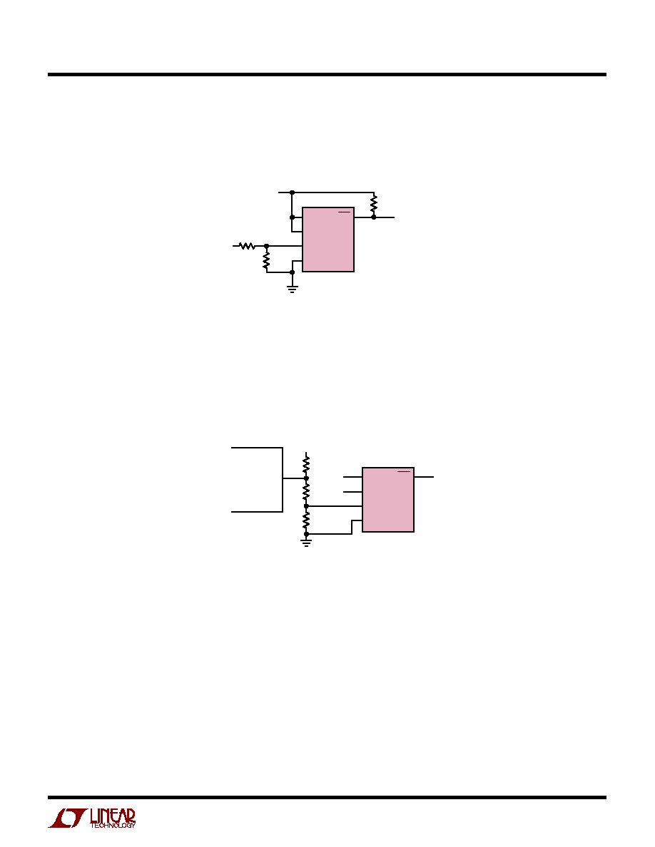
Dual Supply Monitor (3.3V Plus Adjustable)
5
4
3
2
1
V
CC3
V
CC25
V
CCA
GND
RST
LTC1728-2.5
SYSTEM RESET
R2*
1727/28 TA06
R1*
ADJUSTABLE
SUPPLY
3.3V
10k
*TO PRESERVE THRESHOLD ACCURACY, SET PARALLEL
COMBINATION OF R1 AND R2
66.5k
Using V
CCA
Tied to DC/DC Feedback Divider
5
4
3
2
1
V
CC3
V
CC5
V
CCA
GND
RST
LTC1728-5
3.3V
SYSTEM RESET
5V
22.1k
1%
1727/28 TA07
35.7k
1%
LTC1435
ADJUSTABLE
RESET TRIP
THRESHOLD 2.74V
2.9V
2.8k
1%
6
V
OSENSE
14
LTC1727/LTC1728
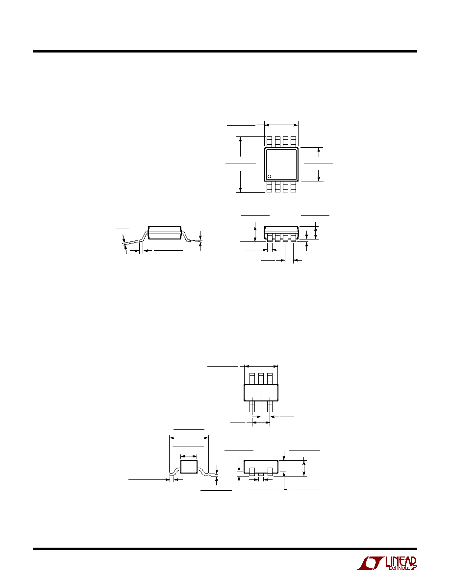
S5 Package
5-Lead Plastic SOT-23
(LTC DWG # 05-08-1633)
PACKAGE DESCRIPTIO
U
Dimensions in inches (millimeters) unless otherwise noted.
0.95
(0.037)
REF
1.50 ≠ 1.75
(0.059 ≠ 0.069)
0.35 ≠ 0.55
(0.014 ≠ 0.022)
0.35 ≠ 0.50
(0.014 ≠ 0.020)
FIVE PLACES (NOTE 2)
S5 SOT-23 0599
2.80 ≠ 3.00
(0.110 ≠ 0.118)
(NOTE 3)
1.90
(0.074)
REF
0.90 ≠ 1.45
(0.035 ≠ 0.057)
0.90 ≠ 1.30
(0.035 ≠ 0.051)
0.00 ≠ 0.15
(0.00 ≠ 0.006)
0.09 ≠ 0.20
(0.004 ≠ 0.008)
(NOTE 2)
2.60 ≠ 3.00
(0.102 ≠ 0.118)
NOTE:
1. DIMENSIONS ARE IN MILLIMETERS
2. DIMENSIONS ARE INCLUSIVE OF PLATING
3. DIMENSIONS ARE EXCLUSIVE OF MOLD FLASH AND METAL BURR
4. MOLD FLASH SHALL NOT EXCEED 0.254mm
5. PACKAGE EIAJ REFERENCE IS SC-74A (EIAJ)
MS8 Package
8-Lead Plastic MSOP
(LTC DWG # 05-08-1660)
MSOP (MS8) 1098
* DIMENSION DOES NOT INCLUDE MOLD FLASH, PROTRUSIONS OR GATE BURRS. MOLD FLASH,
PROTRUSIONS OR GATE BURRS SHALL NOT EXCEED 0.006" (0.152mm) PER SIDE
** DIMENSION DOES NOT INCLUDE INTERLEAD FLASH OR PROTRUSIONS.
INTERLEAD FLASH OR PROTRUSIONS SHALL NOT EXCEED 0.006" (0.152mm) PER SIDE
0.021
±
0.006
(0.53
±
0.015)
0
∞
≠ 6
∞
TYP
SEATING
PLANE
0.007
(0.18)
0.040
±
0.006
(1.02
±
0.15)
0.012
(0.30)
REF
0.006
±
0.004
(0.15
±
0.102)
0.034
±
0.004
(0.86
±
0.102)
0.0256
(0.65)
BSC
1
2
3
4
0.193
±
0.006
(4.90
±
0.15)
8
7 6
5
0.118
±
0.004*
(3.00
±
0.102)
0.118
±
0.004**
(3.00
±
0.102)
15
LTC1727/LTC1728
PACKAGE DESCRIPTIO
U
Dimensions in inches (millimeters) unless otherwise noted.
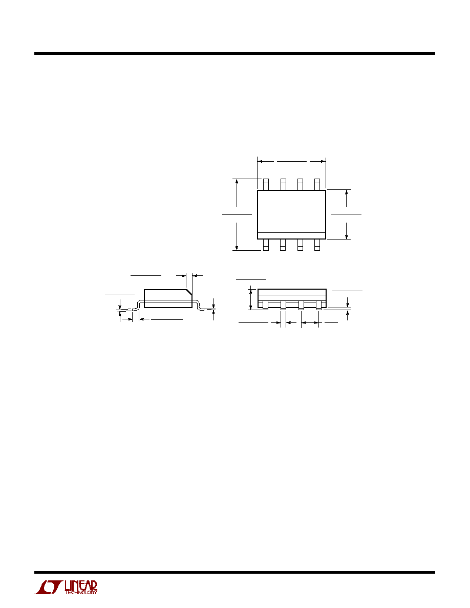
S8 Package
8-Lead Plastic Small Outline (Narrow 0.150)
(LTC DWG # 05-08-1610)
0.016 ≠ 0.050
(0.406 ≠ 1.270)
0.010 ≠ 0.020
(0.254 ≠ 0.508)
◊
45
∞
0
∞
≠ 8
∞
TYP
0.008 ≠ 0.010
(0.203 ≠ 0.254)
SO8 1298
0.053 ≠ 0.069
(1.346 ≠ 1.752)
0.014 ≠ 0.019
(0.355 ≠ 0.483)
TYP
0.004 ≠ 0.010
(0.101 ≠ 0.254)
0.050
(1.270)
BSC
1
2
3
4
0.150 ≠ 0.157**
(3.810 ≠ 3.988)
8
7
6
5
0.189 ≠ 0.197*
(4.801 ≠ 5.004)
0.228 ≠ 0.244
(5.791 ≠ 6.197)
DIMENSION DOES NOT INCLUDE MOLD FLASH. MOLD FLASH
SHALL NOT EXCEED 0.006" (0.152mm) PER SIDE
DIMENSION DOES NOT INCLUDE INTERLEAD FLASH. INTERLEAD
FLASH SHALL NOT EXCEED 0.010" (0.254mm) PER SIDE
*
**
Information furnished by Linear Technology Corporation is believed to be accurate and reliable.
However, no responsibility is assumed for its use. Linear Technology Corporation makes no represen-
tation that the interconnection of its circuits as described herein will not infringe on existing patent rights.
16
LTC1727/LTC1728
©
LINEAR TECHNOLOGY CORPORATION 1999
17278f LT/TP 0400 4K ∑ PRINTED IN THE USA
PART NUMBER
DESCRIPTION
COMMENTS
LTC690
5V Supply Monitor, Watchdog Timer and Battery Backup
4.65V Threshold
LTC694-3.3
3.3V Supply Monitor, Watchdog Timer and Battery Backup
2.9V Threshold
LTC699
5V Supply Monitor and Watchdog Timer
4.65V Threshold
LTC1232
5V Supply Monitor, Watchdog Timer and Push-Button Reset
4.37V/4.62V Threshold
LTC1326
Micropower Precision Triple Supply Monitor for 5V, 3.3V and ADJ
4.725V, 3.118V, 1V Thresholds (
±
0.75%)
LTC1326-2.5
Micropower Precision Triple Supply Monitor for 2.5V, 3.3V and ADJ
2.363V, 3.118V, 1V Thresholds (
±
0.75%)
LTC1443/LTC1444
Micropower Quad Comparators with 1% Reference
LTC1443 Has 1.182V Reference, LTC1444/LTC1445
LTC1445
Have 1.221V Reference and Adjustable Hysteresis
LTC1536
Precision Triple Supply Monitor for PCI Applications
Meets PCI t
FAIL
Timing Specifications
LTC1540
Nanopower Comparator with 2% Reference
1.182V Reference, 300nA Supply Current, 8-Pin MSOP
LTC1726-2.5
Micropower Triple Supply Monitor for 2.5V, 3.3V and ADJ
Adjustable RESET and Watchdog Time Outs
LTC1726-5
Micropower Triple Supply Monitor for 5V, 3.3V and ADJ
Adjustable RESET and Watchdog Time Outs
LTC1985-1.8
Micropower Triple Supply Monitor for 3.3V, 1.8V and ADJ
Push-Pull RESET Output, SOT-23
RELATED PARTS
Linear Technology Corporation
1630 McCarthy Blvd., Milpitas, CA 95035-7417
(408) 432-1900
q
FAX: (408) 434-0507
q
www.linear-tech.com
TYPICAL APPLICATIO
U
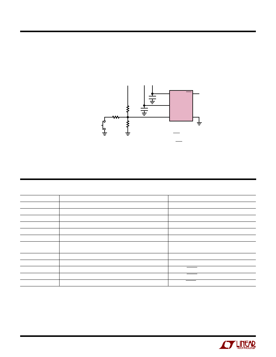
Triple Supply Monitor with Manual Reset Button
V
CC3
V
CC5
V
CCA
RST
GND
LTC1728-5
1727/28 TA02
100nF
5
5V
3.3V
12V (
±
5%)
V
TRIP
= 11.2V
(
±
0.17V)
1
2
R2
105k
0.1%
*OPTIONAL RESISTOR RECOMMENDED
TO EXTEND ESD TOLERANCE
R3*
10k
5%
MANUAL
RESET BUTTON
(NORMALLY OPEN)
4
3
R1
1.07M
0.1%
100nF
V
TRIP
=
(R1 + R2)
R1 = R2
≠ 1
V
CCA
R2
( )
V
TRIP
V
CCA