1
LTC1731-4.2
Lithium-Ion Linear
Battery Charger Controller
December 1999
The LTC
Æ
1731-4.2 is a complete constant-current/con-
stant-voltage linear charge controller for lithium-ion bat-
teries. Nickel-cadmium (NiCd) and nickel-metal-hydride
(NiMH) batteries can also be charged with constant
current using external termination. The external sense
resistor sets the charge current with 5% accuracy. An
internal resistor divider and precision reference set the
final float potential with 1% accuracy. The output float
voltage is set internally to 4.2V.
When the input supply is removed, the LTC1731-4.2
automatically enters a low current sleep mode, dropping
the battery drain current to 5
µ
A. An internal comparator
detects the end-of-charge (C/10) condition while a pro-
grammable timer, using an external capacitor, sets the
total charge time. Fully discharged cells are automatically
trickle charged at 10% of the programmed current until
cell voltage exceeds 2.5V.
The LTC1731-4.2 is available in the 8-pin MSOP and SO
packages.
s
Complete Linear Charger Controller for
1-Cell Lithium-Ion Batteries
s
1% Voltage Accuracy
s
Programmable Charge Current
s
C/10 Charge Current Detection Output
s
Programmable Charge Termination Timer
s
Space Saving 8-Pin MSOP Package
s
Automatic Sleep Mode When Input Supply
is Removed (Only 7
µ
A Battery Drain)
s
Automatic Trickle Charging of Low Voltage Cells
s
Programmable for Constant-Current-Only Mode
s
Cellular Phones
s
Handheld Computers
s
Charging Docks and Cradles
s
Programmable Current Source
, LTC and LT are registered trademarks of Linear Technology Corporation.
FEATURES
DESCRIPTIO
N
U
APPLICATIO
N
S
U
TYPICAL APPLICATIO
N
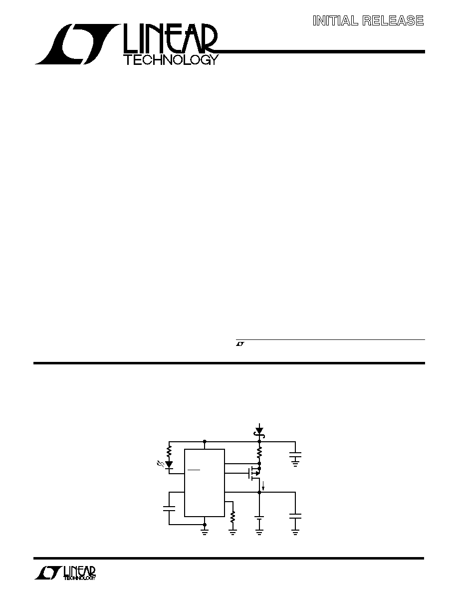
U
V
CC
V
IN
5V TO 15V
SENSE
DRV
1k
R
SENSE
0.2
R
PROG
*
19.6k
Li-ION
CELL
LTC1731-4.2
*SHUTDOWN INVOKED BY FLOATING THE PROG PIN
BAT
CHRG
8
7
MBRM120T3
10
µ
F
1731 TA01
1
µ
F
I
BAT
= 500mA
C
TIMER
0.1
µ
F
Q1
Si9430DY
6
1
5
4
+
2
3
TIMER
PROG
GND
500mA Li-Ion Charger
Information furnished by Linear Technology Corporation is believed to be accurate and reliable.
However, no responsibility is assumed for its use. Linear Technology Corporation makes no represen-
tation that the interconnection of its circuits as described herein will not infringe on existing patent rights.
Final Electrical Specifications
2
LTC1731-4.2
SYMBOL
PARAMETER
CONDITIONS
MIN
TYP
MAX
UNITS
V
CC
Input Supply Voltage
q
4.5
12
V
I
CC
Input Supply Current
Charger On, Current Mode
q
1
3
mA
Shutdown Mode
q
1
2
mA
Sleep Mode (Battery Drain Current)
7
20
µ
A
V
BAT
Regulated Output Voltage
LTC1731-4.2 (5V
V
CC
12V)
q
4.158
4.2
4.242
V
I
BAT
Current Mode Charge Current
R
PROG
= 19.6k, R
SENSE
= 0.2
465
500
535
mA
R
PROG
= 19.6k, R
SENSE
= 0.2
q
415
585
mA
R
PROG
= 97.6k, R
SENSE
= 0.2
70
100
130
mA
I
TRIKL
Trickle Charge Current
V
BAT
= 2V, R
PROG
= 19.6k, I
TRIKL
= (V
CC
≠ V
SENSE
)/0.2
q
30
50
95
mA
V
TRIKL
Trickle Charge Threshold Voltage
From Low to High
q
2.4
2.457
2.55
V
V
UV
V
CC
Undervoltage Lockout Voltage
From Low to High
q
4.1
4.5
V
V
UV
V
CC
Undervoltage Lockout Hysteresis
200
mV
V
MSD
Manual Shutdown Threshold Voltage
PROG Pin Low to High
2.457
V
PROG Pin High to Low
2.446
V
ORDER PART
NUMBER
(Note 1)
Input Supply Voltage (V
CC
) ................................... 13.2V
Input Voltage (SENSE, DRV, BAT,
TIMER, PROG) ....................... ≠ 0.3V to (V
CC
+ 0.3V)
Output Voltage (CHRG) ......................... ≠ 0.3V to 13.2V
LTC1731EMS8-4.2
T
JMAX
= 150
∞
C,
JA
= 180
∞
C/W
Consult factory for Industrial and Military grade parts.
ABSOLUTE
M
AXI
M
U
M
RATINGS
W
W
W
U
PACKAGE/ORDER I
N
FOR
M
ATIO
N
W
U
U
Operating Temperature Range (Note 2) .....≠ 40
∞
to 85
∞
C
Storage Temperature Range ................. ≠ 65
∞
C to 150
∞
C
Lead Temperature (Soldering, 10 sec).................. 300
∞
C
MS8 PART MARKING
LTKQ
1
2
3
4
BAT
CHRG
TIMER
GND
8
7
6
5
SENSE
V
CC
DRV
PROG
TOP VIEW
MS8 PACKAGE
8-LEAD PLASTIC MSOP
ORDER PART
NUMBER
LTC1731ES8-4.2
S8 PART MARKING
173142
The
q
denotes the specifications which apply over the full operating
temperature range, otherwise specifications are at T
A
= 25
∞
C. V
CC
= 6V unless otherwise noted.
ELECTRICAL CHARACTERISTICS
1
2
3
4
8
7
6
5
TOP VIEW
SENSE
V
CC
DRV
PROG
BAT
CHRG
TIMER
GND
S8 PACKAGE
8-LEAD PLASTIC SO
T
JMAX
= 150
∞
C,
JA
= 125
∞
C/W
3
LTC1731-4.2
Note 1: Absolute Maximum Ratings are those values beyond which the life
of a device may be impaired.
SYMBOL
PARAMETER
CONDITIONS
MIN
TYP
MAX
UNITS
V
ASD
Automatic Shutdown Threshold Voltage
(V
CC
≠ V
BAT
) High to Low
30
54
90
mV
(V
CC
≠ V
BAT
) Low to High
40
69
100
mV
V
DIS
Voltage Mode Disable Threshold Voltage
V
TIMER
q
5.6
V
I
PROG
PROG Pin Current
Internal Pull-Up Current, No R
PROG
2.5
µ
A
PROG Pin Load Regulation
PROG Pin Source Current,
V
PROG
5mV
q
300
µ
A
V
PROG
PROG Pin Voltage
R
PROG
=19.6k
2.457
V
I
CHRG
CHRG Pin Weak Pull-Down Current
V
CHRG
= 1V
70
100
130
µ
A
V
CHRG
CHRG Pin Output Low Voltage
I
CHRG
= 5mA
0.6
1.2
V
I
C/10
End of Charge Indication Current Level
R
PROG
= 19.6k, R
SENSE
= 0.2
q
25
50
100
mA
t
TIMER
TIMER Accuracy
C
TIMER
= 0.1
µ
F
10
%
V
CLAMP
DRV Pin Clamp Voltage
V
CLAMP
= V
CC
≠ V
DRV
, I
DRIVE
= 50
µ
A
6.5
V
ELECTRICAL CHARACTERISTICS
PI
N
FU
N
CTIO
N
S
U
U
U
BAT (Pin 1): Battery Sense Input. A bypass capacitor of at
least 10
µ
F is required to keep the loop stable when the
battery is not connected. A precision internal resistor
divider sets the final float potential on this pin. The resistor
divider is disconnected in sleep mode.
CHRG (Pin 2): Open-Drain Charge Status Output. When
the battery is being charged, the CHRG pin is pulled low by
an internal N-channel MOSFET. When the charge current
drops to 10% of the full-scale current for at least 0.32
seconds, the N-channel MOSFET turns off and a 100
µ
A
current source is connected from the CHRG pin to GND.
When the timer runs out or the input supply is removed,
the current source will be disconnected and the CHRG pin
is forced into a high impedance state.
TIMER (Pin 3): Timer Capacitor and Constant-Voltage
Mode Disable Input Pin. The timer period is set by placing
a capacitor, C
TIMER
, to GND. The timer period is t
TIMER
=
(C
TIMER
∑ 3 hours)/(0.1
µ
F). When the TIMER pin is
connected to V
CC
, the constant-voltage mode is disabled
and the chip will operate in constant-current mode only.
Short the TIMER pin to GND to disable the internal timer
function.
GND (Pin 4): Ground.
PROG (Pin 5): Charge Current Program and Shutdown
Input Pin. The charge current is programmed by connect-
ing a resistor, R
PROG
to ground. The charge current is I
BAT
= (V
PROG
∑ 800
)/(R
PROG
∑ R
SENSE
). The IC can be forced
into shutdown by floating the PROG pin and allowing the
internal 2.5
µ
A current source to pull the pin above the
2.457V shutdown threshold voltage.
DRV (Pin 6): Drive Output Pin for the P-Channel MOSFET
or PNP Transistor. The impedance is high at this pin,
therefore, a high gain PNP pass transistor should be used.
The DRV pin is internally clamped to 8V (max) below V
CC
.
V
CC
(Pin 7): Positive Input Supply Voltage. When V
BAT
is
within 54mV of V
CC
, the LTC1731-4.2 is forced into sleep
mode, dropping I
CC
to 7
µ
A. V
CC
ranges from 4.5V to 12V.
Bypass this pin with a 1
µ
F capacitor.
SENSE (Pin 8): Current Sense Input. A sense resistor,
R
SENSE
, must be connected from V
CC
to the SENSE pin.
This resistor is chosen using the following equation:
R
SENSE
= (V
PROG
∑ 800
)/(R
PROG
∑ I
BAT
)
Note 2: The LTC1731-4.2 is guaranteed to meet performance
specifications from 0
∞
C to 70
∞
C. Specifications over the ≠ 40
∞
C to 85
∞
C
operating temperature range are assured by design, characterization and
correlation with statistical process controls. Guaranteed I grade parts are
available, consult factory.
The
q
denotes the specifications which apply over the full operating
temperature range, otherwise specifications are at T
A
= 25
∞
C. V
CC
= 6V unless otherwise noted.
4
LTC1731-4.2
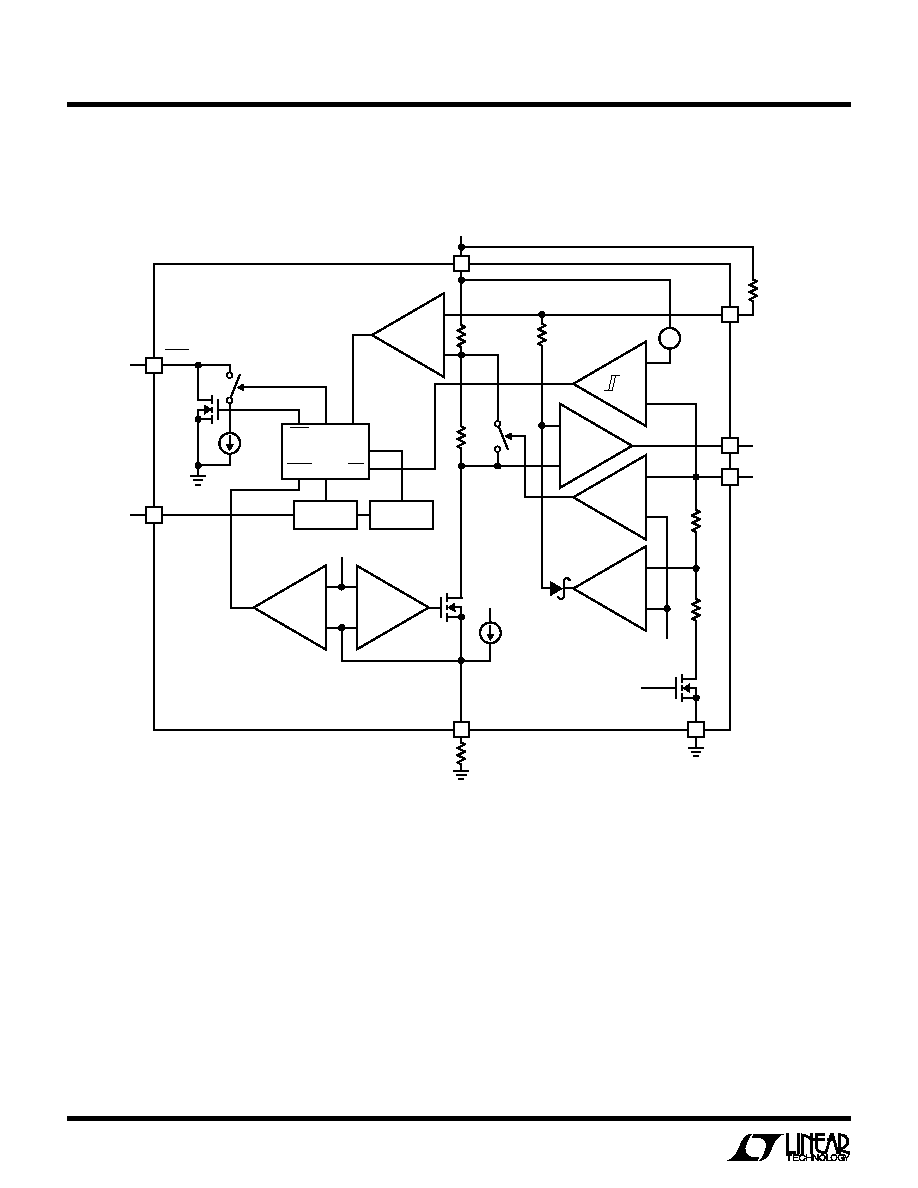
BLOCK DIAGRA
W
≠
+
≠
+
≠
+
≠
+
LOGIC
C1
≠
+
C4
≠
+
≠
+
C3
A1
CA
C2
VA
CHARGE
GND
1731 BD
PROG
BATTERY CURRENT I
BAT
= (2.457V ∑ 800
)/(R
PROG
∑ R
SENSE
)
R
PROG
V
REF
2.457V
LBO
80
V
CC
800
54mV
R
SENSE
SENSE
DRV
BAT
720
100
µ
A
TIMER
OSCILLATOR
V
REF
COUNTER
STOP
SHDN
SLP
C/10
C/10
2.5
µ
A
V
CC
CHRG
4
5
2
3
8
7
6
1
+
≠

5
LTC1731-4.2
OPERATIO
U
The LTC1731-4.2 is a linear battery charger controller. The
charge current is programmed by the combination of a
program resistor (R
PROG
) from the PROG pin to ground
and a sense resistor (R
SENSE
) between the V
CC
and SENSE
pins. R
PROG
sets a program current through an internal
trimmed 800
resistor setting up a voltage drop from V
CC
to the input of the current amplifier (CA). The current
amplifier servos the gate of the external P-channel MOSFET
to force the same voltage drop across R
SENSE
which sets
the charge current. When the potential at the BAT pin
approaches the preset float voltage, the voltage amplifier
(VA) will start sinking current which shrinks the voltage
drop across R
SENSE
, thus reducing the charge current.
Charging begins when the potential at V
CC
pin rises above
the UVLO level and a program resistor is connected from
the PROG pin to ground. At the beginning of the charge
cycle, if the battery voltage is below 2.457V per cell, the
charger goes into trickle charge mode. The trickle charge
current is 10% of the full-scale current. If the cell voltage
stays low for one quarter of the total charge time, the
charge sequence will be terminated immediately.
The charger goes into the fast charge constant-current
mode after the voltage on the BAT pin rises above 2.457V
per cell. In constant-current mode, the charge current is
set by the combination of R
SENSE
and R
PROG
.
When the battery approaches the final float voltage, the
charge current will begin to decrease. When the current
drops to 10% of the full-scale charge current, an internal
comparator will turn off the pull-down N-channel MOSFET
at the CHRG pin and connect a weak current source to
ground to indicate an end-of-charge (C/10) condition.
An external capacitor on the TIMER pin sets the total
charge time. After a time-out occurs, the charging will be
terminated immediately and the CHRG pin is forced to a
high impedance state. To restart the charge cycle, simply
remove the input voltage and reapply it, or float the PROG
pin momentarily.
For batteries like lithium-ion that require accurate final
float potential, the internal 2.457V reference, voltage
amplifier and the resistor divider provide regulation with
±
1% (max) accuracy. For NiMH and NiCd batteries, the
LTC1731-4.2 can be turned into a current source by
pulling the TIMER pin to V
CC
. When in the constant-
current only mode, the voltage amplifier, timer and the
trickle charge function are all disabled.
When the input voltage is not present, the charger goes
into a sleep mode, dropping I
CC
to 5
µ
A. This greatly
reduces the current drain on the battery and increases the
standby time. The charger can be shut down by floating the
PROG pin. An internal current source will pull it high and
clamp at 3.5V.
APPLICATIO
N
S I
N
FOR
M
ATIO
N
W
U
U
U
Charge Termination
The charger is off when any of the following conditions
exist: the voltage at the V
CC
pin is below 4.1V, the voltage
at the V
CC
pin is higher than 4.1V but is less than 54mV
above V
BAT
, or the PROG pin is floating. The DRV pin will
be pulled to V
CC
and the internal resistor divider is discon-
nected to reduce the current drain on the battery.
Undervoltage Lockout (UVLO)
An internal undervoltage lockout circuit monitors the input
voltage and keeps the charger in shutdown mode until V
CC
rises above 4.1V. To prevent oscillation around
V
CC
= 4.1V, the UVLO circuit has built-in hysteresis.
Trickle Charge and Defective Battery Detection
At the beginning of the charging sequence, if the battery
voltage is low (below 2.457V per cell) the charger goes
into trickle mode. The charge current is dropped to 10% of
the full-scale current. If the low cell voltage persists for one
quarter of the total charging time, the battery is considered
defective, the charging will be terminated and the CHRG
pin output is forced to a high impedance state.
Shutdown
The LTC1731-4.2 can be forced into shutdown by float-
ing the PROG pin and allowing the internal 2.5
µ
A current
source to pull the pin above the 2.457V shutdown
6
LTC1731-4.2
threshold voltage. The DRV pin will then be pulled up to
V
CC
and turn off the external P-channel MOSFET. The
internal timer is reset in the shutdown mode.
Programming Charge Current
The formula for the battery charge current (see Block
Diagram) is:
I
BAT
= (I
PROG
)(800
/R
SENSE
)
= (2.457V/R
PROG
)(800
/R
SENSE
)
where R
PROG
is the total resistance from the PROG pin to
ground.
For example, if 0.5A charge current is needed, select a
value for R
SENSE
that will drop 100mV at the maximum
charge current. R
SENSE
= 0.1V/0.5A = 0.2
, then calculate:
R
PROG
= (2.457V/500mA)(800
/0.2
) = 19.656k
For best stability over temperature and time, 1% resistors
are recommended. The closest 1% resistor value is 19.6k.
Programming the Timer
The programmable timer is used to terminate the charge.
The length of the timer is programmed by an external
capacitor at the TIMER pin. The total charge time is:
Time = (3 Hours)(C
TIMER
/0.1
µ
F)
The timer starts when the input voltage greater than 4.1V
is applied and the program resistor is connected to ground.
After a time-out occurs, the CHRG output will turn into a
high impedance state to indicate that the charging has
stopped. Connecting the TIMER pin to V
CC
disables the
timer and also puts the charger into a constant-current
mode. To only disable the timer function, short the TIMER
pin to GND.
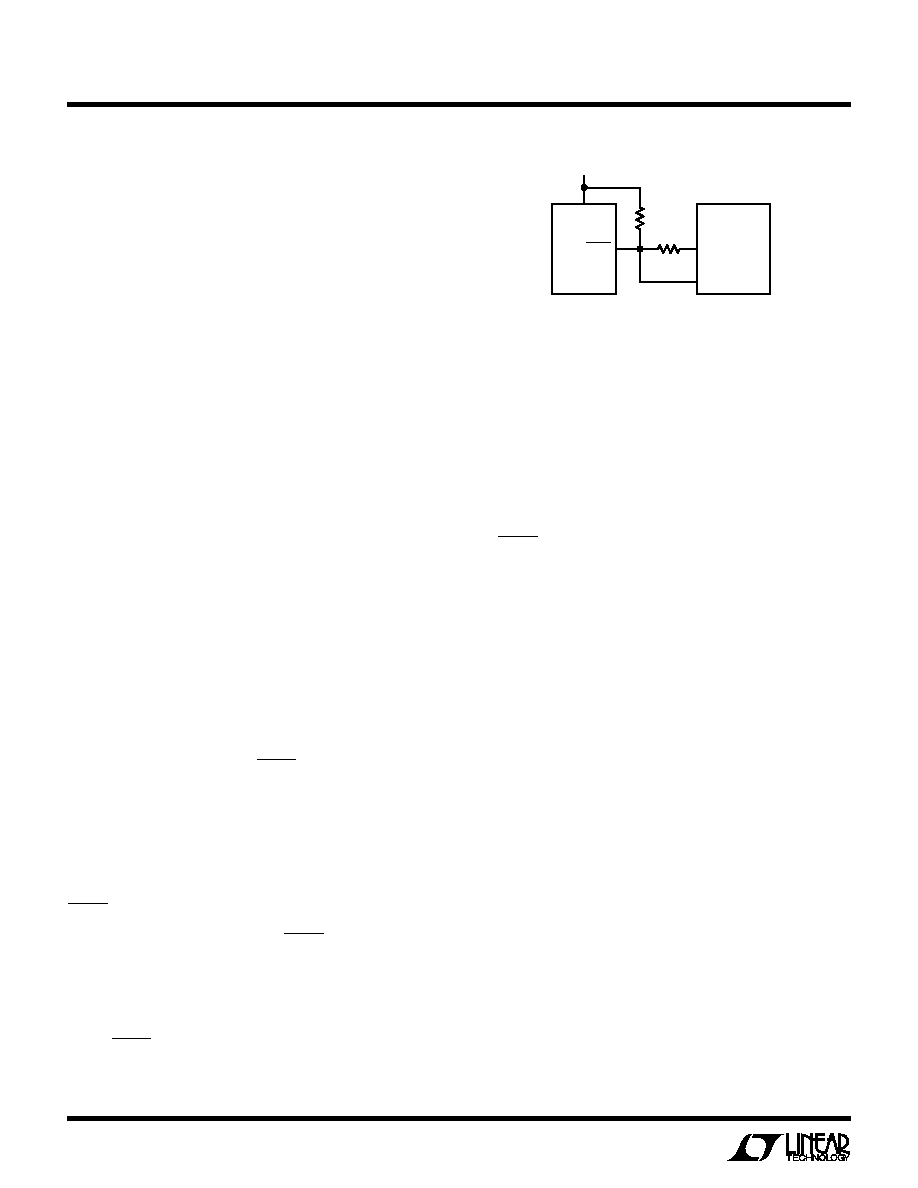
CHRG Status Output Pin
When the charge cycle starts, the CHRG pin is pulled down
to ground by an internal N-channel MOSFET that can drive
an LED. When the battery current drops to 10% of the full-
scale current (C/10), the N-channel MOSFET is turned off
and a weak 100
µ
A current source to ground is connected
to the CHRG pin. After a time-out occurs, the pin will go
into a high impedance state. By using two different value
pull-up resistors, a microprocessor can detect three states
APPLICATIO
N
S I
N
FOR
M
ATIO
N
W
U
U
U
from this pin (charging, C/10 and stop charging). See
Figure 1.
End of Charge (C/10)
The LTC1731-4.2 includes a comparator to monitor the
charge current to detect an end-of-charge condition. When
the battery current falls below 10% of full scale, the
comparator trips and turns off the N-channel MOSFET at
the CHRG pin and switches in a 100
µ
A current source to
ground. After an internal time delay of 300ms, this state is
then latched. This delay will help prevent false triggering
due to transient currents. The end-of-charge comparator
is disabled in trickle charge mode.
Gate Drive
Typically the LTC1731-4.2 controls an external P-channel
MOSFET to supply current to the battery. The DRV pin is
internally clamped to 6.5V below V
CC
. This feature allows
low voltage P-channel MOSFETs with gate to source
breakdown voltage rated at 8V to be used.
An external PNP transistor can also be used as the pass
transistor instead of the P-channel MOSFET. Due to the
low current gain of the current amplifier (CA), a high gain
Darlington PNP transistor is required to avoid too much
charging current error. The gain of the current amplifier is
around 0.6
µ
A/mV. For every 1
µ
A of base current, a 1.6mV
of gain error shows up at the inputs of CA. With R
PROG
=
19.6k (100mV across R
SENSE
), it represents 1.67% of
error in charging current.
Constant-Current Only Mode
The LTC1731-4.2 can be used as a programmable current
source by forcing the TIMER pin to V
CC
. This is particu-
larly useful for charging NiMH or NiCd batteries. In the
1k
100k
CHRG
1731 F01
V
CC
LTC1731-4.2
V
+
I/O
µ
PROCESSOR
I/O
2
7
Figure 1. Microprocessor Interface
7
LTC1731-4.2
constant-current only mode, the timer and voltage ampli-
fier are both disabled. An external termination method is
required to properly terminate the charge.
Stability
The charger is stable without any compensation when a
P-channel MOSFET is used as the pass transistor.
However, a 10
µ
F capacitor is recommended at the BAT
APPLICATIO
N
S I
N
FOR
M
ATIO
N
W
U
U
U
pin to keep the ripple voltage low when the battery is
disconnected.
When a PNP transistor is chosen as the pass transistor, a
1000pF capacitor is required from the DRV pin to V
CC
. This
capacitor is needed to help stablize the voltage loop. A
10
µ
F capacitor at the BAT pin is also recommended when
a battery is not present.
V
CC
V
IN
5V TO 15V
SENSE
DRV
R2
1k
R
SENSE
0.2
R1
10k
R
PROG
19.6k
Li-ION
CELL
LTC1731-4.2
BAT
CHRG
8
7
MBRM120T3
C2
10
µ
F
C1
1nF
1731 TA02
C3
1
µ
F
I
BAT
= 500mA
+
C
TIMER
0.1
µ
F
Q1
2N5087
6
1
5
4
2
3
TIMER
PROG
GND
Q2
ZTX749
TYPICAL APPLICATIO
N
U
Linear Charger Using a PNP Transistor
Dimensions in inches (millimeters) unless otherwise noted.
PACKAGE DESCRIPTIO
N
U
S8 Package
8-Lead Plastic Small Outline (Narrow 0.150)
(LTC DWG # 05-08-1610)
0.016 ≠ 0.050
(0.406 ≠ 1.270)
0.010 ≠ 0.020
(0.254 ≠ 0.508)
◊
45
∞
0
∞
≠ 8
∞
TYP
0.008 ≠ 0.010
(0.203 ≠ 0.254)
SO8 1298
0.053 ≠ 0.069
(1.346 ≠ 1.752)
0.014 ≠ 0.019
(0.355 ≠ 0.483)
TYP
0.004 ≠ 0.010
(0.101 ≠ 0.254)
0.050
(1.270)
BSC
1
2
3
4
0.150 ≠ 0.157**
(3.810 ≠ 3.988)
8
7
6
5
0.189 ≠ 0.197*
(4.801 ≠ 5.004)
0.228 ≠ 0.244
(5.791 ≠ 6.197)
DIMENSION DOES NOT INCLUDE MOLD FLASH. MOLD FLASH
SHALL NOT EXCEED 0.006" (0.152mm) PER SIDE
DIMENSION DOES NOT INCLUDE INTERLEAD FLASH. INTERLEAD
FLASH SHALL NOT EXCEED 0.010" (0.254mm) PER SIDE
*
**
8
LTC1731-4.2
1731is, sn1731 LT/TP 1299 4K ∑ PRINTED IN USA
Dimensions in inches (millimeters) unless otherwise noted.
PACKAGE DESCRIPTIO
N
U
PART NUMBER
DESCRIPTION
COMMENTS
LT
Æ
1510-5
500kHz Constant-Voltage/Constant-Current Battery Charger
Most Compact, Up to 1.5A, Charges NiCd, NiMH, Li-Ion Cells
LT1512
SEPIC Battery Charger
V
IN
Can Be Higher or Lower Than Battery Voltage, 1.5A Switch
LT1620
Rail-to-Rail Current Sense Amplifier
Precise Output Current Programming, Up to 32V V
OUT
, Up to 10A I
OUT
LTC1729
Termination Controller for Li-Ion
Time or Charge Current Termination, Automatic Charger/Battery
Detection, Status Output, Preconditioning, 8-Lead MSOP
RELATED PARTS
TYPICAL APPLICATIO
N
U
Low Dropout Linear Charger
V
CC
V
IN
4.5V
SENSE
DRV
R1
50k
R
SENSE
0.2
R
PROG
19.6k
Li-ION
CELL
+
LTC1731-4.2
BAT
CHRG
8
7
C2
10
µ
F
1731 TA03
C1
1
µ
F
I
BAT
= 500mA
C
TIMER
0.1
µ
F
Q2
1/2 Si9934DY
Q1
1/2 Si9934DY
6
1
5
4
2
3
TIMER
PROG
GND
MS8 Package
8-Lead Plastic MSOP
(LTC DWG # 05-08-1660)
Linear Technology Corporation
1630 McCarthy Blvd., Milpitas, CA 95035-7417
(408) 432-1900
q
FAX: (408) 434-0507
q
www.linear-tech.com
MSOP (MS8) 1098
* DIMENSION DOES NOT INCLUDE MOLD FLASH, PROTRUSIONS OR GATE BURRS. MOLD FLASH,
PROTRUSIONS OR GATE BURRS SHALL NOT EXCEED 0.006" (0.152mm) PER SIDE
** DIMENSION DOES NOT INCLUDE INTERLEAD FLASH OR PROTRUSIONS.
INTERLEAD FLASH OR PROTRUSIONS SHALL NOT EXCEED 0.006" (0.152mm) PER SIDE
0.021
±
0.006
(0.53
±
0.015)
0
∞
≠ 6
∞
TYP
SEATING
PLANE
0.007
(0.18)
0.040
±
0.006
(1.02
±
0.15)
0.012
(0.30)
REF
0.006
±
0.004
(0.15
±
0.102)
0.034
±
0.004
(0.86
±
0.102)
0.0256
(0.65)
BSC
1
2
3
4
0.193
±
0.006
(4.90
±
0.15)
8
7 6
5
0.118
±
0.004*
(3.00
±
0.102)
0.118
±
0.004**
(3.00
±
0.102)
© LINEAR TECHNOLOGY CORPORATION 1999