 | –≠–ª–µ–∫—Ç—Ä–æ–Ω–Ω—ã–π –∫–æ–º–ø–æ–Ω–µ–Ω—Ç: LTC1735 | –°–∫–∞—á–∞—Ç—å:  PDF PDF  ZIP ZIP |
LT3724
1
3724f
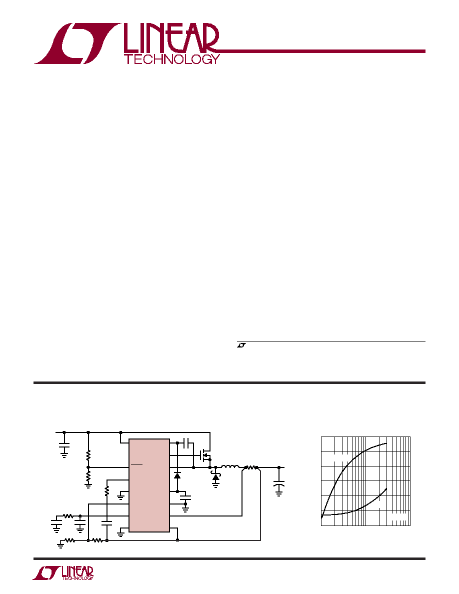
TYPICAL APPLICATIO
U
APPLICATIO S
U
FEATURES
DESCRIPTIO
U
Industrial Power Distribution
12V and 42V Automotive and Heavy Equipment
High Voltage Single Board Systems
Distributed Power Systems
Avionics
Telecom Power
Wide Input Range: 4V to 60V
Output Voltages up to 36V (Step-Down)
Burst Mode
Æ
Operation: <100µA Supply Current
<10µA Shutdown Supply Current
±1.3% Reference Accuracy
200kHz Fixed Frequency
Drives N-Channel MOSFET
Programmable Soft-Start
Programmable Undervoltage Lockout
Internal High Voltage Regulator for Gate Drive
Thermal Shutdown
Current Limit Unaffected by Duty Cycle
16-Pin Thermally Enhanced TSSOP Package
High Voltage, Current Mode
Switching Regulator Controller
Efficiency and Power Loss
vs Load Current
High Voltage Step-Down Regulator
LOAD CURRENT (A)
0.1
EFFICIENCY (%)
POWER LOSS (W)
95
90
85
80
75
70
65
12
10
8
6
4
2
0
1
10
3724 TA01b
V
IN
= 48V
LOSS
EFFICIENCY
V
IN
SHDN
C
SS
Burst_EN
V
FB
V
C
SGND
BOOST
TG
SW
V
CC
PGND
SENSE
+
SENSE
≠
V
IN
30V TO
60V
V
OUT
24V
75W
3724 TA01a
LT3724
1M
68.1k
1000pF
4.99k
93.1k
200k
0.22µF
C
OUT
330µF
C
IN
68µF
1µF
47µH
0.025
Si7852
SS3H9
120pF
680pF
40.2k
+
The LT
Æ
3724 is a DC/DC controller used for medium
power, low part count, low cost, high efficiency supplies.
It offers a wide 4V-60V input range (7.5V minimum startup
voltage) and can implement step-down, step-up, inverting
and SEPIC topologies.
The LT3724 includes Burst Mode operation, which re-
duces quiescent current below 100µA and maintains high
efficiency at light loads. An internal high voltage bias
regulator allows for simple biasing and can be back driven
to increase efficiency.
Additional features include fixed frequency current mode
control for fast line and load transient response; a gate
driver capable of driving large N-channel MOSFETs; a
precision undervoltage lockout function; 10µA shutdown
current; short-circuit protection; and a programmable
soft-start function that directly controls output voltage
slew rates at startup which limits inrush current, mini-
mizes overshoot and facilitates supply sequencing.
The LT3724 is available in a 16-lead thermally enhanced
TSSOP package.
, LTC and LT are registered trademarks of Linear Technology Corporation.
Burst Mode is a registered trademark of Linear Technology Corporation.
All other trademarks are the property of their respective owners.
Protected by U.S. Patents including 5731694, 6498466, 6611131.

LT3724
2
3724f
Input Supply Voltage (V
IN
)......................... 65V to ≠0.3V
Boosted Supply Voltage (BOOST) .............. 80V to ≠0.3V
Switch Voltage (SW) .................................... 65V to ≠1V
Differential Boost Voltage
(BOOST to SW) ..................................... 24V to ≠0.3V
Bias Supply Voltage (V
CC
) ......................... 24V to ≠0.3V
SENSE
+
and SENSE
≠
Voltages ................... 40V to ≠0.3V
Differential Sense Voltage
(SENSE
+
to SENSE
≠
) .................................. 1V to ≠1V
BURST_EN Voltage .................................... 24V to ≠0.3V
V
C
, V
FB
, C
SS
, and SHDN Voltages ................ 5V to ≠0.3V
C
SS
and SHDN Pin Currents .................... 1mA to ≠1mA
Operating Junction Temperature Range (Note 2)
LT3724E (Note 3) ..............................≠40∞C to 125∞C
LT3724I .............................................≠40∞C to 125∞C
Storage Temperature .............................≠65∞C to 150∞C
Lead Temperature (Soldering, 10 sec).................. 300∞C
ORDER PART
NUMBER
T
JMAX
= 125∞C,
JA
= 40∞C/W,
JC
= 10∞C/W
EXPOSED PAD IS SGND (PIN 17)
MUST BE SOLDERED TO PCB
LT3724EFE
LT3724IFE
ABSOLUTE AXI U
RATI GS
W
W
W
U
PACKAGE/ORDER I FOR ATIO
U
U
W
(Note 1)
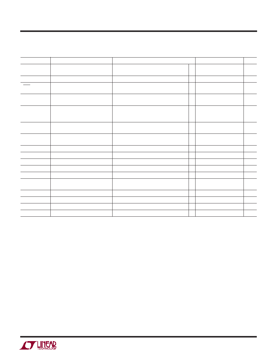
ELECTRICAL CHARACTERISTICS
The
denotes the specifications which apply over the full operating
temperature range, otherwise specifications are at T
A
= 25∞C. V
IN
= 20V, V
CC
= BOOST = BURST_EN = 10V, SHDN = 2V,
SENSE
≠
= SENSE
+
= 10V, SGND = PGND = SW = 0V, unless otherwise noted.
SYMBOL
PARAMETER
CONDITIONS
MIN
TYP
MAX
UNITS
V
IN
Operating Voltage Range (Note 4)
4
60
V
Minimum Start Voltage
7.5
V
UVLO Threshold (Falling)
3.65
3.8
3.95
V
UVLO Threshold Hysteresis
670
mV
I
VIN
V
IN
Supply Current
V
CC
> 9V
20
µA
V
IN
Burst Mode Current
V
BURST_EN
= 0V, V
FB
= 1.35V
20
µA
V
IN
Shutdown Current
V
SHDN
= 0V
9
15
µA
V
BOOST
Operating Voltage Range
75
V
Operating Voltage Range (Note 5)
V
BOOST
- V
SW
20
V
UVLO Threshold (Rising)
V
BOOST
- V
SW
5
V
UVLO Threshold Hysteresis
V
BOOST
- V
SW
400
mV
I
BOOST
BOOST Supply Current (Note 6)
1.4
mA
BOOST Burst Mode Current
V
BURST_EN
= 0V
0.1
µA
BOOST Shutdown Current
V
SHDN
= 0V
0.1
µA
V
CC
Operating Voltage Range (Note 5)
20
V
Output Voltage
Over Full Line and Load Range
8
8.3
V
UVLO Threshold (Rising)
6.25
V
UVLO Threshold Hysteresis
500
mV
I
VCC
V
CC
Supply Current (Note 6)
1.7
2.1
mA
V
CC
Burst Mode Current
V
BURST_EN
= 0V
80
µA
V
CC
Shutdown Current
V
SHDN
= 0V
20
µA
Short-Circuit Current
≠30
≠55
mA
Consult LTC Marketing for parts specified with wider operating temperature ranges.
FE PACKAGE
16-LEAD PLASTIC TSSOP
1
2
3
4
5
6
7
8
TOP VIEW
16
15
14
13
12
11
10
9
V
IN
NC
SHDN
C
SS
BURST_EN
V
FB
V
C
SGND
BOOST
TG
SW
NC
V
CC
PGND
SENSE
+
SENSE
≠
17
FE PART
MARKING
3724EFE
3724IFE
LT3724
3
3724f
Note 1: Absolute Maximum Ratings are those values beyond which the life
of a device may be impaired.
Note 2: The LT3724 includes overtemperature protection that is intended
to protect the device during momentary overload conditions. Junction
temperature will exceed 125∞C when overtemperature protection is active.
Continuous operation above the specified maximum operating junction
temperature may impair device reliability.
Note 3: The LT3724E is guaranteed to meet performance specifications
from 0∞C to 125∞C junction temperature. Specifications over the ≠ 40∞C to
125∞C operating junction temperature range are assured by design,
characterization and correlation with statistical process controls. The
LT3724I is guaranteed over the full ≠40∞C to 125∞C operating junction
temperature range.
ELECTRICAL CHARACTERISTICS
The
denotes the specifications which apply over the full operating
temperature range, otherwise specifications are at T
A
= 25∞C. V
IN
= 20V, V
CC
= BOOST = BURST_EN = 10V, SHDN = 2V,
SENSE
≠
= SENSE
+
= 10V, SGND = PGND = SW = 0V, unless otherwise noted.
Note 4: V
IN
voltages below the start-up threshold (7.5V) are only
supported when the V
CC
is externally driven above 6.5V.
Note 5: Operating range is dictated by MOSFET absolute maximum V
GS
.
Note 6: Supply current specification does not include switch drive
currents. Actual supply currents will be higher.
Note 7: DC measurement of gate drive output "ON" voltage is typically
8.6V. Internal dynamic bootstrap operation yields typical gate "ON"
voltages of 9.8V during standard switching operation. Standard operation
gate "ON" voltage is not tested but guaranteed by design.
SYMBOL
PARAMETER
CONDITIONS
MIN
TYP
MAX
UNITS
V
FB
Error Amp Reference Voltage
Measured at V
FB
Pin
1.224
1.231
1.238
V
1.215
1.245
V
I
FB
Feedback Input Current
25
nA
V
SHDN
Enable Threshold (Rising)
1.3
1.35
1.4
V
Threshold Hysteresis
120
mV
V
SENSE
Common Mode Range
0
36
V
Current Limit Sense Voltage
V
SENSE
+
≠ V
SENSE
≠
140
150
175
mV
I
SENSE
Input Current
V
SENSE(CM)
= 0V
400
µA
(I
SENSE
+
+ I
SENSE
≠
)
2V < V
SENSE(CM)
< 3.5V
2
µA
V
SENSE(CM)
> 4V
≠150
µA
f
SW
Operating Frequency
190
200
210
kHz
175
220
kHz
V
FB(SS)
Soft-Start Disable Voltage
V
FB
Rising
1.185
V
Soft-Start Disable Hysteresis
300
mV
I
SS
Soft-Start Capacitor Control Current
2
µA
g
m
Error Amp Transconductance
275
340
400
µmhos
A
V
Error Amp DC Voltage Gain
62
dB
V
C
Error Amp Output Range
Zero Current to Current Limit
1.2
V
I
VC
Error Amp Sink/Source Current
±30
µA
V
TG
Gate Drive Output On Voltage (Note 7) C
LOAD
= 3300pF
9.8
V
Gate Drive Output Off Voltage
C
LOAD
= 3300pF
0.1
V
t
TG
Gate Drive Rise/Fall Time
10% to 90% or 90% to 10%, C
LOAD
= 3300pF
60
ns
t
TG(OFF)
Minimum Switch Off Time
350
ns
t
TG(ON)
Minimum Switch On Time
300
500
ns
I
SW
SW Pin Sink Current
V
SW
= 2V
300
mA
LT3724
4
3724f
3724 G01
SHUTDOWON THRESHOLD, RISING (V)
1.38
1.37
1.36
1.35
1.34
1.33
1.32
3724 G04
TEMPERATURE (∞C)
≠50
25
75
3724 G02
≠25
0
50
100
125
TEMPERATURE (∞C)
≠50
SHUTDOWON THRESHOLD, FALLING (V)
1.26
1.25
1.24
1.23
1.22
1.21
1.20
25
75
≠25
0
50
100
125
I
CC (LOAD)
(mA)
0
8.2
8.1
8.0
7.9
7.8
7.7
7.6
7.5
15
25
3724 G05
5
10
20
30
35
V
CC
(V)
V
IN
(V)
V
CC
(V)
9
8
7
6
5
4
3
4
6
8
9
5
7
10
11
12
3724 G07
TEMPERATURE (∞C)
≠50
25
75
≠25
0
50
100
125
3724 G08
V
CC
UVLO THRESHOLD, RISING (V)
6.5
6.4
6.3
6.2
6.1
6.0
TEMPERATURE (∞C)
≠50
ERROR AMP TRANSCONDUCTANCE (
µ
Mhos)
350
345
340
335
330
325
320
25
75
3724 G09
≠25
0
50
100
125
T
A
= 25∞C
I
CC
= 20mA
T
A
= 25∞C
TEMPERATURE (∞C)
≠50
25
75
≠25
0
50
100
125
3724 G03
8.2
8.1
8.0
7.9
7.8
7.7
7.6
7.5
V
CC
(V)
I
CC
= 20mA
TEMPERATURE (∞C)
≠50
25
75
≠25
0
50
100
125
3724 G06
I
CC
CURRENT LIMIT (mA)
70
60
50
40
30
20
V
CC
(V)
0
I
CC
(
µ
A)
15
20
25
16
10
5
0
2
4
6
8
10 12 14
18 20
T
A
= 25∞C
TYPICAL PERFOR A CE CHARACTERISTICS
U
W
Shutdown Threshold (Rising)
vs Temperature
Shutdown Threshold (Falling)
vs Temperature
V
CC
vs Temperature
V
CC
vs I
CC(LOAD)
V
CC
vs V
IN
I
CC
Current Limit vs Temperature
V
CC
UVLO Threshold (Rising)
vs Temperature
Error Amp Transconductance
vs Temperature
I
CC
vs V
CC
(SHDN = 0V)

LT3724
5
3724f
TYPICAL PERFOR A CE CHARACTERISTICS
U
W
I
(SENSE
+
+ SENSE
≠
)
vs
V
SENSE (CM)
Operating Frequency
vs Temperature
Error Amp Reference
vs Temperature
Maximum Current Sense
Threshold vs Temperature
V
IN
UVLO Threshold (Rising)
vs Temperature
V
IN
UVLO Threshold (Falling)
vs Temperature
V
SENSE (CM)
(V)
0
I
(SENSE
+
+ SENSE
≠
)
(
µ
A)
400
300
200
100
0
≠100
≠200
0.5 1.0 1.5 2.0
3724 G10
2.5
4.5
3.5
5.0
4.0
3.0
TEMPERATURE (∞C)
≠50
OPERATING FREQUENCY (kHz)
230
220
210
200
190
180
170
25
75
3724 G11
≠25
0
50
100
125
TEMPERATURE (∞C)
≠50
25
75
3724 G12
≠25
0
50
100
125
TEMPERATURE (∞C)
≠50
25
75
≠25
0
50
100
125
TEMPERATURE (∞C)
≠50
25
75
≠25
0
50
100
125
TEMPERATURE (∞C)
≠50
25
75
≠25
0
50
100
125
1.234
1.233
1.232
1.231
1.230
1.229
1.228
1.227
ERROR AMP REFERENCE (V)
CURRENT SENSE THRESHOLD (mV)
160
158
156
154
152
150
148
146
144
142
140
3724 G13
3724 G14
3724 G15
4.54
4.52
4.50
4.48
4.46
4.44
4.42
4.40
V
IN
UVLO THRESHOLD, RISING (V)
V
IN
UVLO THRESHOLD, FALLING (V)
3.86
3.84
3.82
3.80
3.78
3.76
T
A
= 25∞C