 | ÐлекÑÑоннÑй компоненÑ: LTC1735IF | СкаÑаÑÑ:  PDF PDF  ZIP ZIP |
1735fb.pm65
1
LTC1735
1735fb
High Efficiency
Synchronous Step-Down Switching Regulator
The LTC
®
1735 is a synchronous step-down switching
regulator controller that drives external N-channel power
MOSFETs using a fixed frequency architecture. Burst
Mode
TM
operation provides high efficiency at low load
currents. The precision 0.8V reference is compatible with
future microprocessor generations. OPTI-LOOP compen-
sation allows the transient response to be optimized over
a wide range of output capacitance and ESR values.
The operating frequency (synchronizable up to 500kHz) is
set by an external capacitor allowing maximum flexibility
in optimizing efficiency. A forced continuous control pin
reduces noise and RF interference and can assist second-
ary winding regulation by disabling Burst Mode operation
when the main output is lightly loaded.
Protection features include internal foldback current lim-
iting, output overvoltage crowbar and optional short-
circuit shutdown. Soft-start is provided by an external
capacitor that can be used to properly sequence supplies.
The operating current level is user-programmable via an
external current sense resistor. Wide input supply range
allows operation from 3.5V to 30V (36V maximum).
s
Synchronizable/Programmable Fixed Frequency
s
OPTI-LOOP
TM
Compensation Minimizes C
OUT
s
±
1% Output Voltage Accuracy
s
Dual N-Channel MOSFET Synchronous Drive
s
Wide V
IN
Range: 3.5V to 36V Operation
s
V
OUT
Range: 0.8V to 6V
s
Internal Current Foldback
s
Output Overvoltage Crowbar Protection
s
Latched Short-Circuit Shutdown Timer
with Defeat Option
s
Very Low Dropout Operation: 99% Duty Cycle
s
Forced Continuous Control Pin
s
Optional Programmable Soft-Start
s
Remote Output Voltage Sense
s
Power Good Output (LTC1735F Only)
s
Logic Controlled Micropower Shutdown: I
Q
< 25
µ
A
s
LTC1435 Pin Compatible with
Minor Component Changes
s
Available in 16-Lead Narrow SSOP, SO Packages and
20-Lead TSSOP Package (LTC1735F Only)
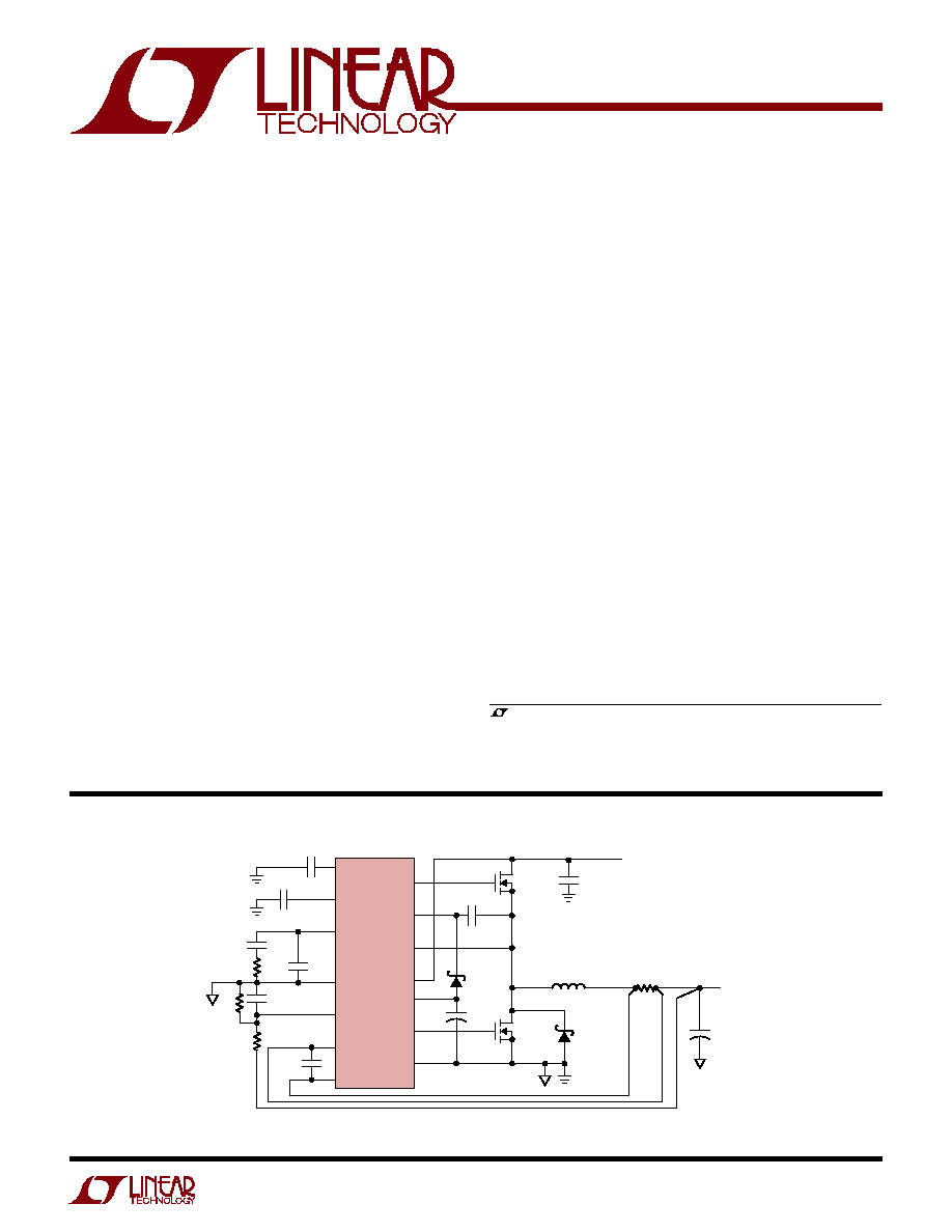
Figure 1. High Efficiency Step-Down Converter
, LTC and LT are registered trademarks of Linear Technology Corporation.
Burst Mode and OPTI-LOOP are trademarks of Linear Technology Corporation.
s
Notebook and Palmtop Computers, PDAs
s
Cellular Telephones and Wireless Modems
s
DC Power Distribution Systems
C
OSC
RUN/SS
I
TH
TG
BOOST
SW
V
IN
LTC1735
C
B
0.22
µ
F
100pF
C
C
330pF
R
C
33k
R
SENSE
0.005
V
OUT
1.6V
9A
C
OUT
: PANASONIC EEFUEOG181R
C
IN
: MARCON THCR70E1H226ZT
L1: PANASONIC ETQP6F2R0HFA
R
SENSE
: IRC LRF2010-01-R005J
1000pF
C
SS
0.1
µ
F
C
OSC
47pF
+
4.7
µ
F
+
C
OUT
180
µ
F
4V
×
4
SP
C
IN
22
µ
F
50V
M1
FDS6680A
M2
FDS6680A
1735 F01
D
B
CMDSH-3
D1
MBRS340T3
V
IN
5V TO 24V
L1
2
µ
H
C
C2
100pF
R2
20k
1%
R1
20k
1%
SGND
V
OSENSE
SENSE
SENSE
+
INTV
CC
BG
PGND
FEATURES
DESCRIPTIO
U
APPLICATIO S
U
TYPICAL APPLICATIO
U
2
LTC1735
1735fb
ABSOLUTE AXI U
RATI GS
W
W
W
U
Input Supply Voltage (V
IN
).........................36V to 0.3V
Topside Driver Supply Voltage (BOOST)....42V to 0.3V
Switch Voltage (SW) ....................................36V to 5V
EXTV
CC
Voltage ...........................................7V to 0.3V
Boosted Driver Voltage (BOOST SW) .......7V to 0.3V
SENSE
+
, SENSE
Voltages .......... 1.1 (INTV
CC
) to 0.3V
FCB Voltage ............................(INTV
CC
+ 0.3V) to 0.3V
I
TH
, V
OSENSE
Voltages ............................... 2.7V to 0.3V
RUN/SS, PGOOD (LTC1735F Only)
Voltages .......................................................7V to 0.3V
ELECTRICAL CHARACTERISTICS
The
q
denotes specifications which apply over the full operating
temperature range, otherwise specifications are at T
A
= 25
°
C. V
IN
= 15V, V
RUN/SS
= 5V unless otherwise noted.
Peak Driver Output Current <10
µ
s (TG, BG) .............. 3A
INTV
CC
Output Current ......................................... 50mA
Operating Ambient Temperature Range
LTC1735C ............................................... 0
°
C to 85
°
C
LTC1735I/LTC1735E (Note 8) ............ 40
°
C to 85
°
C
Junction Temperature (Note 2) ............................. 125
°
C
Storage Temperature Range ................. 65
°
C to 150
°
C
Lead Temperature (Soldering, 10 sec).................. 300
°
C
(Note 1)
PACKAGE/ORDER I FOR ATIO
U
U
W
ORDER PART
NUMBER
LTC1735CGN
LTC1735CS
LTC1735IGN
LTC1735IS
LTC1735EGN
T
JMAX
= 125
°
C,
JA
= 130
°
C/W (GN)
T
JMAX
= 125
°
C,
JA
= 110
°
C/W (S)
TOP VIEW
S PACKAGE
16-LEAD PLASTIC SO
GN PACKAGE
16-LEAD NARROW
PLASTIC SSOP
1
2
3
4
5
6
7
8
16
15
14
13
12
11
10
9
C
OSC
RUN/SS
I
TH
FCB
SGND
V
OSENSE
SENSE
SENSE
+
TG
BOOST
SW
V
IN
INTV
CC
BG
PGND
EXTV
CC
GN PART MARKING
1735
1735I
1735E
Consult LTC marketing for parts specified with wider operating temperature ranges.
ORDER PART
NUMBER
LTC1735CF
LTC1735IF
T
JMAX
= 125
°
C,
JA
= 110
°
C/W
1
2
3
4
5
6
7
8
9
10
TOP VIEW
F PACKAGE
20-LEAD PLASTIC TSSOP
20
19
18
17
16
15
14
13
12
11
NC
C
OSC
RUN/SS
I
TH
FCB
SGND
V
OSENSE
PGOOD
SENSE
SENSE
+
NC
TG
BOOST
SW
V
IN
INTV
CC
BG
PGND
EXTV
CC
NC
SYMBOL
PARAMETER
CONDITIONS
MIN
TYP
MAX
UNITS
Main Control Loop
I
VOSENSE
Feedback Current
(Note 3)
4
25
nA
V
OSENSE
Feedback Voltage
(Note 3)
q
0.792
0.8
0.808
V
V
LINEREG
Reference Voltage Line Regulation
V
IN
= 3.6V to 30V (Note 3)
0.001
0.02
%/V
V
LOADREG
Output Voltage Load Regulation
(Note 3)
Measured in Servo Loop; V
ITH
= 0.7V
q
0.1
0.3
%
Measured in Servo Loop; V
ITH
= 2V
q
0.1
0.3
%
DF Max
Maximum Duty Factor
In Dropout
98
99.4
%
g
m
Transconductance Amplifier g
m
1.3
mmho
V
FCB
Forced Continuous Threshold
q
0.76
0.8
0.84
V
I
FCB
Forced Continuous Current
V
FCB
= 0.85V
0.17
0.3
µ
A
3
LTC1735
1735fb
SYMBOL
PARAMETER
CONDITIONS
MIN
TYP
MAX
UNITS
ELECTRICAL CHARACTERISTICS
The
q
denotes specifications which apply over the full operating
temperature range, otherwise specifications are at T
A
= 25
°
C. V
IN
= 15V, V
RUN/SS
= 5V unless otherwise noted.
V
OVL
Feedback Overvoltage Lockout
q
0.84
0.86
0.88
V
I
Q
Input DC Supply Current
(Note 4)
Normal Mode
450
µ
A
Shutdown
V
RUN/SS
= 0V
15
25
µ
A
V
RUN/SS
Run Pin Start Threshold
V
RUN/SS
, Ramping Positive
1.0
1.5
1.9
V
V
RUN/SS
Run Pin Begin Latchoff Threshold
V
RUN/SS
, Ramping Positive
4.1
4.5
V
I
RUN/SS
Soft-Start Charge Current
V
RUN/SS
= 0V
0.7
1.2
µ
A
I
SCL
RUN/SS Discharge Current
Soft Short Condition, V
OSENSE
= 0.5V,
0.5
2
4
µ
A
V
RUN/SS
= 4.5V
UVLO
Undervoltage Lockout
Measured at V
IN
Pin (V
IN
Ramping Down)
q
3.5
3.9
V
V
SENSE(MAX)
Maximum Current Sense Threshold
V
OSENSE
= 0.7V
q
60
75
85
mV
I
SENSE
Sense Pins Total Source Current
V
SENSE
= V
SENSE
+
= 0V
60
80
µ
A
t
ON(MIN)
Minimum On-Time
Tested with a Square Wave (Note 6)
160
200
ns
TG Transition Time:
(Note 7)
TG t
r
Rise Time
C
LOAD
= 3300pF
50
90
ns
TG t
f
Fall Time
C
LOAD
= 3300pF
50
90
ns
BG Transition Time:
(Note 7)
BG t
r
Rise Time
C
LOAD
= 3300pF
50
90
ns
BG t
f
Fall Time
C
LOAD
= 3300pF
40
80
ns
TG/BG t
1D
Top Gate Off to Synchronous
C
LOAD
= 3300pF Each Driver
100
ns
Gate On Delay Time
TG/BG t
2D
Synchronous Gate Off to Top
C
LOAD
= 3300pF Each Driver
70
ns
Gate On Delay Time
Internal V
CC
Regulator
V
INTVCC
Internal V
CC
Voltage
6V < V
IN
< 30V, V
EXTVCC
= 4V
5.0
5.2
5.4
V
V
LDO(INT)
Internal V
CC
Load Regulation
I
CC
= 0 to 20mA, V
EXTVCC
= 4V
0.2
1
%
V
LDO(EXT)
EXTV
CC
Drop Voltage
I
CC
= 20mA, V
EXTVCC
= 5V
130
200
mV
V
EXTVCC
EXTV
CC
Switchover Voltage
I
CC
= 20mA, EXTV
CC
Ramping Positive
q
4.5
4.7
V
V
EXTVCC(HYS)
EXTV
CC
Hysteresis
0.2
V
Oscillator
f
OSC
Oscillator Frequency
C
OSC
= 43pF (Note 5)
265
300
335
kHz
f
H
/f
OSC
Maximum Sync Frequency Ratio
1.3
f
FCB(SYNC)
FCB Pin Threshold For Sync
Ramping Negative
0.9
1.2
V
PGOOD Output (LTC1735F Only)
V
PGL
PGOOD Voltage Low
I
PGOOD
= 2mA
110
200
mV
I
PGOOD
PGOOD Leakage Current
V
PGOOD
= 5V
±
1
µ
A
V
PG
PGOOD Trip Level
V
OSENSE
with Respect to Set Output Voltage
V
OSENSE
Ramping Negative
6.0
7.5
9.5
%
V
OSENSE
Ramping Positive
6.0
7.5
9.5
%
Note 1: Absolute Maximum Ratings are those values beyond which the life
of a device may be impaired.
Note 2: T
J
is calculated from the ambient temperature T
A
and power
dissipation P
D
according to the following formulas:
LTC1735CS, LTC1735IS: T
J
= T
A
+ (P
D
· 110
°
C/W)
LTC1735CGN, LTC1735IGN, LTC1735EGN: T
J
= T
A
+ (P
D
· 130
°
C/W)
LTC1735CF, LTC1735IF: T
J
= T
A
+ (P
D
· 110
°
C/W)
4
LTC1735
1735fb
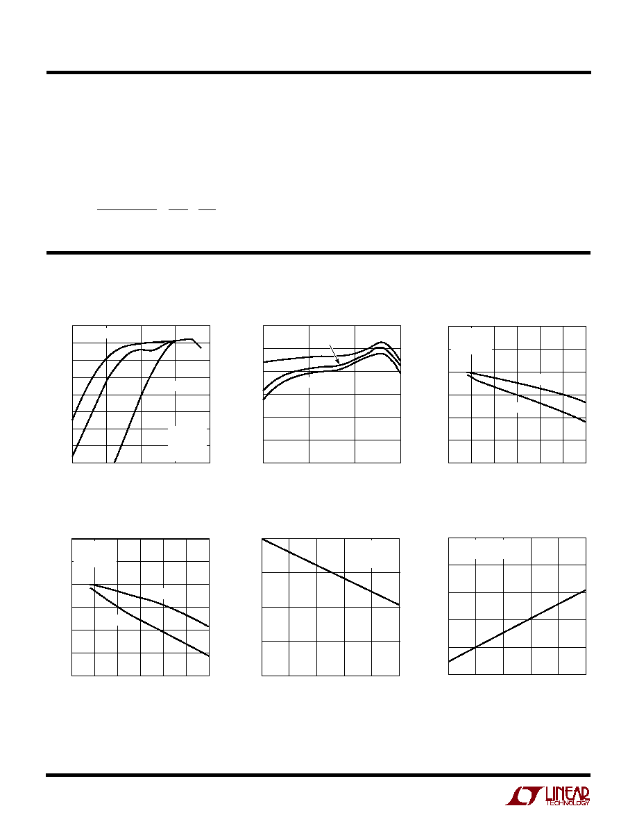
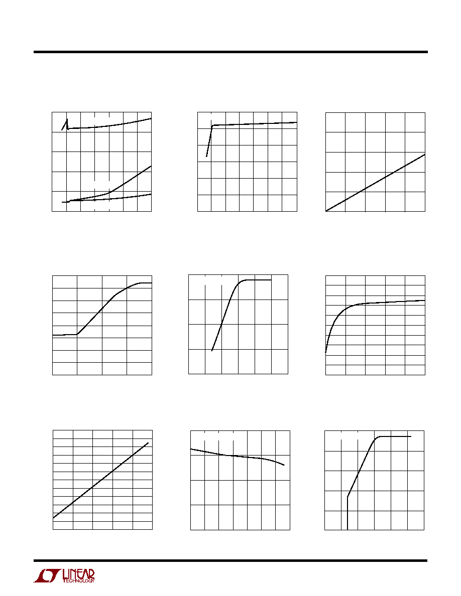
TYPICAL PERFOR A CE CHARACTERISTICS
U
W
Efficiency vs Load Current
(3 Operating Modes)
Efficiency vs Load Current
Efficiency vs Input Voltage
LOAD CURRENT (A)
0.001
EFFICIENCY (%)
60
70
80
BURST
SYNC
10
1735 G01
50
40
20
0.01
0.1
1
30
100
90
V
IN
= 10V
V
OUT
= 3.3V
R
S
= 0.01
f
O
= 300kHz
EXTV
CC
OPEN
CONTINUOUS
LOAD CURRENT (A)
0.01
0.1
1
10
EFFICIENCY (%)
1735 G02
100
90
80
70
60
50
40
V
IN
= 5V
EXTV
CC
= 5V
FIGURE 1
V
IN
= 24V
V
IN
= 15V
INPUT VOLTAGE (V)
0
70
EFFICIENCY (%)
75
80
85
90
100
5
10
15
20
1735 G03
25
30
95
EXTV
CC
= 5V
V
OUT
= 1.6V
FIGURE 1
I
OUT
= 5A
I
OUT
= 0.5A
Efficiency vs Input Voltage
Load Regulation
V
IN
V
OUT
Dropout Voltage
vs Load Current
INPUT VOLTAGE (V)
0
70
EFFICIENCY (%)
75
80
85
90
100
5
10
15
20
1735 G04
25
30
95
EXTV
CC
OPEN
V
OUT
= 1.6V
FIGURE 1
I
OUT
= 5A
I
OUT
= 0.5A
LOAD CURRENT (A)
0
NORMALIZED V
OUT
(%)
0.2
0.1
8
1735 G05
0.3
0.4
2
4
6
10
0
FCB = 0V
V
IN
= 15V
FIGURE 1
LOAD CURRENT (A)
0
0
V
IN
V
OUT
(mV)
500
400
300
200
100
2
4
6
8
1735 G06
10
R
SENSE
= 0.005
V
OUT
= 5V 5% DROP
Note 3: The LTC1735 is tested in a feedback loop that servos V
OSENSE
to
the balance point for the error amplifier (V
ITH
= 1.2V).
Note 4: Dynamic supply current is higher due to the gate charge being
delivered at the switching frequency. See Applications Information.
Note 5: Oscillator frequency is tested by measuring the C
OSC
charge
current (I
OSC
) and applying the formula:
f
C
pF
I
I
OSC
OSC
CHG
DIS
=
+
+
8 477 10
11
1
1
11
1
.
(
)
( )
Note 6: The minimum on-time condition corresponds to an inductor peak-
to-peak ripple current
40% of I
MAX
(see Minimum On-Time
Considerations in the Applications Information section).
Note 7: Rise and fall times are measured using 10% and 90% levels. Delay
times are measured using 50% levels.
Note 8: The LTC1735E is guaranteed to meet performance specifications
from 0
°
C to 85
°
C. Specifications over the 40
°
C to 85
°
C operating
temperature range are assured by design, characterization and correlation
with statistical process controls. The LTC1735I specifications are
guaranteed over the full 40
°
C to 85
°
C operating temperature range.
ELECTRICAL CHARACTERISTICS
5
LTC1735
1735fb
Maximum Current Sense Threshold
vs Normalized Output Voltage
(Foldback)
TYPICAL PERFOR A CE CHARACTERISTICS
U
W
Maximum Current Sense Threshold
vs V
RUN/SS
Maximum Current Sense Threshold
vs Sense Common Mode Voltage
Maximum Current Sense Threshold
vs I
TH
Voltage
V
ITH
vs V
RUN/SS
Maximum Current Sense Threshold
vs Temperature
NORMALIZED OUTPUT VOLTAGE (%)
0
MAXIMUM CURRENT SENSE THRESHOLD (mV)
40
50
60
100
1735 G10
30
20
0
25
50
75
10
80
70
V
RUN/SS
(V)
0
0
MAXIMUM CURRENT SENSE THRESHOLD (mV)
20
40
60
80
1
2
3
4
1735 G11
5
6
V
SENSE(CM)
= 1.6V
COMMON MODE VOLTAGE (V)
0
MAXIMUM CURRENT SENSE THRESHOLD (mV)
72
76
80
4
1735 G12
68
64
60
1
2
3
5
V
ITH
(V)
0
MAXIMUM CURRENT SENSE THRESHOLD (mV)
30
50
70
90
2
1735 G13
10
10
20
40
60
80
0
20
30
0.5
1
1.5
2.5
V
RUN/SS
(V)
0
0
V
ITH
(V)
0.5
1.0
1.5
2.0
2.5
1
2
3
4
1735 G15
5
6
V
OSENSE
= 0.7V
TEMPERATURE (
°
C)
40
60
MAXIMUM CURRENT SENSE THRESHOLD (mV)
65
70
75
80
15
10
35
60
1735 G18
85
110
135
V
SENSE(CM)
= 1.6V
Input and Shutdown Currents
vs Input Voltage
INTV
CC
Line Regulation
INPUT VOLTAGE (V)
0
5
0
INPUT CURRENT (
µ
A)
SHUTDOWN CURRENT (
µ
A)
200
500
10
20
25
1735 G07
100
400
300
0
40
100
20
80
60
15
30
35
EXTV
CC
OPEN
SHUTDOWN
EXTV
CC
= 5V
INPUT VOLTAGE (V)
0
INTV
CC
VOLTAGE (V)
4
5
6
15
25
1735 G08
3
2
5
10
20
30
35
1
0
1mA LOAD
EXTV
CC
Switch Drop
vs INTV
CC
Load Current
INTV
CC
LOAD CURRENT (mA)
0
EXTV
CC
INTV
CC
(mV)
300
400
500
40
1735 G09
200
100
0
10
20
30
50