 | –≠–ª–µ–∫—Ç—Ä–æ–Ω–Ω—ã–π –∫–æ–º–ø–æ–Ω–µ–Ω—Ç: LTC1736C | –°–∫–∞—á–∞—Ç—å:  PDF PDF  ZIP ZIP |

1
LTC1736
5-Bit Adjustable
High Efficiency Synchronous
Step-Down Switching Regulator
Figure 1. High Efficiency Step-Down Converter
s
Dual N-Channel MOSFET Synchronous Drive
s
Synchronizable/Programmable Fixed Frequency
s
Wide V
IN
Range: 3.5V to 36V Operation
s
5-Bit Digital-to-Analog V
OUT
Selection:
0.925V to 2.00V Range with 50mV/25mV Steps
s
OPTI-LOOP
TM
Compensation Minimizes C
OUT
s
±
1% Output Voltage Accuracy
s
Power Good Output Voltage Monitor
s
Active Voltage Positioning Compatible
s
Output Overvoltage Crowbar Protection
s
Internal Current Foldback
s
Latched Short-Circuit Shutdown Timer
with Defeat Option
s
Forced Continuous Control Pin
s
Optional Programmable Soft-Start
s
Remote Output Voltage Sense
s
Available in 24-Lead SSOP Package
s
Notebook and Palmtop Computers, PDAs
s
Power Supply for Mobile Pentium
Æ
II and
Pentium III Processors
s
Low Voltage Power Supplies
The LTC
Æ
1736 is a synchronous step-down switching
regulator controller optimized for CPU power. The output
voltage is programmed by a 5-bit digital-to-analog con-
verter (DAC) that adjusts the output voltage from 0.925V
to 2.00V according to Intel mobile VID specifications. The
0.8V reference is compatible with future microprocessor
generations.
The operating frequency (synchronizable up to 500kHz) is
set by an external capacitor allowing maximum flexibility
in optimizing efficiency. The output voltage is monitored by
a power good window comparator that indicates when the
output is within 7.5% of its programmed value.
Protection features include: internal foldback current lim-
iting, output overvoltage crowbar and optional short-cir-
cuit shutdown. Soft-start is provided by an external capaci-
tor that can be used to properly sequence supplies. The
operating current level is user-programmable via an exter-
nal current sense resistor. Wide input supply range allows
operation from 3.5V to 30V (36V maximum).
Pin defeatable Burst Mode
TM
operation provides high effi-
ciency at low load currents. OPTI-LOOP compensation
allows the transient response to be optimized over a wide
range of output capacitance and ESR values.
, LTC and LT are registered trademarks of Linear Technology Corporation.
OPTI-LOOP and Burst Mode are trademarks of Linear Technology Corporation.
Pentium is a registered trademark of Intel Corporation.
V
OSENSE
I
TH
47pF
C
C1
330pF
C
B
0.22
µ
F
D
B
CMDSH-3
V
IN
5V TO 24V
C
OSC
47pF
RUN/SS
PGND
BG
1000pF
BOOST
SW
VIDV
CC
INTV
CC
4.7
µ
F
M2
FDS6680A
◊
2
M1
FDS6680A
C
OUT
: PANASONIC EEFUEOG181R
C
IN
: MARCON THCR70EIH226ZT
L1: PANASONIC ETQP6RZIR20HFA
R
SENSE
: IRC LRF2010-01-R004J
D1
MBRS340T3
1736 F01
C
SS
0.1
µ
F
C
C2
47pF
C
OSC
R
C
33k
R
SENSE
0.004
PGOOD
VID4
VID3
VID2
VID1
VID0
SGND
SENSE
≠
LTC1736
SENSE
+
TG
V
IN
+
C
OUT
180
µ
F/4V
◊
4
C
IN
22
µ
F/50V
◊
2
CERAMIC
V
OUT
1.35V TO 1.60V
12A
+
L1
1.2
µ
H
FEATURES
DESCRIPTIO
U
APPLICATIO S
U
TYPICAL APPLICATIO
U
2
LTC1736
ABSOLUTE AXI U
RATI GS
W
W
W
U
PACKAGE/ORDER I FOR ATIO
U
U
W
(Note 1)
Input Supply Voltage (V
IN
).........................36V to ≠ 0.3V
Topside Driver Supply Voltage (BOOST)....42V to ≠ 0.3V
Switch Voltage (SW) ....................................36V to ≠ 5V
EXTV
CC
, VIDV
CC
, (BOOST ≠ SW) Voltages .. 7V to ≠ 0.3V
SENSE
+
, SENSE
≠
.......................... 1.1(INTV
CC
) to ≠ 0.3V
FCB Voltage ............................(INTV
CC
+ 0.3V) to ≠ 0.3V
I
TH
, V
OSENSE
, V
FB
Voltage .........................2.7V to ≠ 0.3V
RUN/SS, VID0 to VID4, PGOOD Voltages ....7V to ≠ 0.3V
Peak Driver Output Current <10
µ
s (TG, BG) .............. 3A
INTV
CC
Output Current ......................................... 50mA
Operating Ambient Temperature Range
LTC1736C ............................................... 0
∞
C to 85
∞
C
LTC1736I ............................................ ≠ 40
∞
C to 85
∞
C
Junction Temperature (Note 2) ............................. 125
∞
C
Storage Temperature Range ................. ≠ 65
∞
C to 150
∞
C
Lead Temperature (Soldering, 10 sec).................. 300
∞
C
ORDER PART
NUMBER
Consult factory for Military grade parts.
T
JMAX
= 125
∞
C,
JA
= 110
∞
C/W
1
2
3
4
5
6
7
8
9
10
11
12
TOP VIEW
G PACKAGE
24-LEAD PLASTIC SSOP
24
23
22
21
20
19
18
17
16
15
14
13
C
OSC
RUN/SS
I
TH
FCB
SGND
PGOOD
SENSE
≠
SENSE
+
V
FB
V
OSENSE
VID0
VID1
TG
BOOST
SW
V
IN
INTV
CC
BG
PGND
EXTV
CC
VIDV
CC
VID4
VID3
VID2
ELECTRICAL CHARACTERISTICS
LTC1736CG
LTC1736IG
The
q
denotes specifications which apply over the full operating
temperature range, otherwise specifications are at T
A
= 25
∞
C. V
IN
= 15V, V
RUN/SS
= 5V unless otherwise noted.
SYMBOL
PARAMETER
CONDITIONS
MIN
TYP
MAX
UNITS
Main Control Loop
V
OSENSE
Output Voltage Set Accuracy
(Note 3) See Table 1
q
1
%
V
LINEREG
Reference Voltage Line Regulation
V
IN
= 3.6V to 30V (Note 3)
0.001
0.02
%/V
V
LOADREG
Output Voltage Load Regulation
(Note 3)
Measured in Servo Loop; V
ITH
= 0.7V
q
0.1
0.3
%
Measured in Servo Loop; V
ITH
= 2V
q
≠ 0.1
≠ 0.3
%
g
m
Transconductance Amplifier g
m
1.3
mmho
V
FCB
Forced Continuous Threshold
q
0.76
0.8
0.84
V
I
FCB
Forced Continuous Current
V
FCB
= 0.85V
≠ 0.17
≠ 0.3
µ
A
V
OVL
Feedback Overvoltage Lockout
q
0.84
0.86
0.88
V
I
Q
Input DC Supply Current
(Note 4)
Normal Mode
450
µ
A
Shutdown
V
RUN/SS
= 0V
15
25
µ
A
V
RUN/SS
Run Pin Start Threshold
V
RUN/SS
, Ramping Positive
1.0
1.5
1.9
V
V
RUN/SS
Run Pin Begin Latchoff Threshold
V
RUN/SS
, Ramping Positive
4.1
4.5
V
I
RUN/SS
Soft-Start Charge Current
V
RUN/SS
= 0V
≠ 0.7
≠ 1.2
µ
A
I
SCL
RUN/SS Discharge Current
Soft Short Condition, V
FB
= 0.5V,
0.5
2
4
µ
A
V
RUN/SS
= 4.5V
UVLO
Undervoltage Lockout
Measured at V
IN
Pin (V
IN
Ramping Down)
q
3.5
3.9
V
V
SENSE(MAX)
Maximum Current Sense Threshold
V
FB
= 0.7V
q
60
75
85
mV
I
SENSE
SENSE Pins Total Source Current
V
SENSE
≠
= V
SENSE
+
= 0.8V
60
80
µ
A
t
ON(MIN)
Minimum On-Time
Tested with a Square Wave (Note 8)
160
200
ns
TG Transition Time:
(Note 9)
TG t
r
Rise Time
C
LOAD
= 3300pF
50
90
ns
TG t
f
Fall Time
C
LOAD
= 3300pF
50
90
ns
3
LTC1736
ELECTRICAL CHARACTERISTICS
The
q
denotes specifications which apply over the full operating
temperature range, otherwise specifications are at T
A
= 25
∞
C. V
IN
= 15V, V
RUN/SS
= 5V unless otherwise noted.
Note 1: Absolute Maximum Ratings are those values beyond which the life
of a device may be impaired.
Note 2: T
J
is calculated from the ambient temperature T
A
and power
dissipation P
D
according to the following formulas:
LTC1736CG, LTC1736IG: T
J
= T
A
+ (P
D
∑ 110
∞
C/W)
Note 3: The LTC1736 is tested in a feedback loop that servos V
FB
to the
balance point for the error amplifier (V
ITH
= 1.2V).
Note 4: Dynamic supply current is higher due to the gate charge being
delivered at the switching frequency. See Applications Information.
Note 5: Oscillator frequency is tested by measuring the C
OSC
charge
current (I
OSC
) and applying the formula:
Note 6: With all five VID inputs floating (or tied to VIDV
CC
) the VIDV
CC
current is typically < 1
µ
A. However, the VIDV
CC
current will rise and be
approximately equal to the number of grounded VID input pins times
(VIDV
CC
≠ 0.6V)/40k. (See the Applications Information section for more
detail.)
Note 7: Each built-in pull-up resistor attached to the VID inputs also has a
series diode to allow input voltages higher than the VIDV
CC
supply without
damage or clamping. (See the Applications Information section for more
detail.)
Note 8: The minimum on-time condition corresponds to the on inductor
peak-to-peak ripple current
40% of I
MAX
(see minimum on-time
considerations in the Applications Information section).
Note 9: Rise and fall times are measured using 10% and 90% levels. Delay
times are measured using 50% levels.
f
C
pF
I
I
OSC
OSC
CHG
DIS
=
+
+
8 477 10
11
1
1
11
1
.
(
)
(
)
≠
SYMBOL
PARAMETER
CONDITIONS
MIN
TYP
MAX
UNITS
BG Transition Time:
(Note 9)
BG t
r
Rise Time
C
LOAD
= 3300pF
50
90
ns
BG t
f
Fall Time
C
LOAD
= 3300pF
40
80
ns
TG/BG T1D
Top Gate Off to Synchronous
C
LOAD
= 3300pF Each Driver
100
ns
Gate-On Delay Time
TG/BG T2D
Synchronous Gate Off to Top
C
LOAD
= 3300pF Each Driver
70
ns
Gate-On Delay Time
Internal V
CC
Regulator
V
INTVCC
Internal V
CC
Voltage
6V < V
IN
< 30V, V
EXTVCC
= 4V
5.0
5.2
5.4
V
V
LDO(INT)
Internal V
CC
Load Regulation
I
CC
= 0mA to 20mA, V
EXTVCC
= 4V
0.2
1
%
V
LDO(EXT)
EXTV
CC
Drop Voltage
I
CC
= 20mA, V
EXTVCC
= 5V
130
200
mV
V
EXTVCC
EXTV
CC
Switchover Voltage
I
CC
= 20mA, EXTV
CC
Ramping Positive
q
4.5
4.7
V
V
EXTVCC(HYS)
EXTV
CC
Hysteresis
0.2
V
Oscillator
f
OSC
Oscillator Frequency
(Note 5), C
OSC
= 43pF
265
300
335
kHz
f
H
/f
OSC
Maximum Sync Frequency Ratio
1.3
f
FCB(SYNC)
FCB Pin Threshold For Sync
Ramping Negative
0.9
1.2
V
PGOOD Output
V
PGL
PGOOD Voltage Low
I
PGOOD
= 2mA
110
200
mV
I
PGOOD
PGOOD Leakage Current
V
PGOOD
= 5V
±
1
µ
A
V
PG
PGOOD Trip Level
V
OSENSE
with Respect to Set Output Voltage
V
OSENSE
Ramping Negative
≠ 6.0
≠ 7.5
≠ 9.5
%
V
OSENSE
Ramping Positive
6.0
7.5
9.5
%
VID Control
VIDV
CC
VID Operating Supply Voltage
2.7
5.5
V
I
VIDVCC
VID Supply Current
(Note 6) VIDV
CC
= 3.3V
0.01
5
µ
A
R
VFB/VOSENSE
Resistance Between V
OSENSE
and V
FB
10
k
R
RATIO
Resistor Ratio Accuracy
Programmed from 0.925V to 2.00V
±
0.05
%
R
PULL-UP
VID0 to VID4 Pull-Up Resistance
(Note 7) V
DIODE
= 0.6V
40
k
V
IDT
VID Input Voltage Threshold
0.4
1.0
1.6
V
I
VIDLEAK
VID Input Leakage Current
(Note 7) VIDV
CC
< VID < 7V
0.01
±
1
µ
A
V
PULL-UP
VID Pull-Up Voltage
VIDV
CC
= 3.3V
2.8
V
VIDV
CC
= 5V
4.5
V
4
LTC1736
TYPICAL PERFOR A CE CHARACTERISTICS
U
W
Efficiency vs Load Current
(3 Operating Modes)
LOAD CURRENT (A)
0.001
EFFICIENCY (%)
60
70
80
BURST
SYNC
CONT
10
1736 G01
50
40
20
0.01
0.1
1
30
100
90
V
IN
= 5V
V
OUT
= 1.6V
R
S
= 0.01
f
O
= 300kHz
EXTV
CC
OPEN
LOAD CURRENT (A)
10mA
100mA
1A
10A
EFFICIENCY (%)
1736 G02
100
90
80
70
60
50
40
V
IN
= 5V
EXTV
CC
= 5V
V
IN
= 24V
V
IN
= 15V
INPUT VOLTAGE (V)
0
70
EFFICIENCY (%)
75
80
85
90
100
5
10
15
20
1736 G03
25
30
95
EXTV
CC
= 5V
V
OUT
= 1.6V
FIGURE 1
I
OUT
= 5A
I
OUT
= 0.5A
Efficiency vs Load Current
Efficiency vs Input Voltage
Efficiency vs Input Voltage
INPUT VOLTAGE (V)
0
70
EFFICIENCY (%)
75
80
85
90
100
5
10
15
20
1736 G04
25
30
95
EXTV
CC
OPEN
V
OUT
= 1.6V
FIGURE 1
I
OUT
= 5A
I
OUT
= 0.5A
LOAD CURRENT (A)
0
NORMALIZED V
OUT
(%)
≠0.2
≠0.1
8
1736 G05
≠0.3
≠0.4
2
4
6
12
10
0
FCB = 0V
V
IN
= 15V
FIGURE 1
Load Regulation
LOAD CURRENT (A)
0
0
I
TH
VOLTAGE (V)
0.5
1.0
1.5
2.0
2.5
1
2
3
4
1736 G06
5
6
V
IN
= 5V
V
OUT
= 1.6V
R
SENSE
= 0.01
f
O
= 300kHz
CONTINUOUS
MODE
Burst Mode
OPERATION
SYNCHRONIZED f = f
O
I
TH
Voltage vs Load Current
Input and Shutdown Currents
vs Input Voltage
INPUT VOLTAGE (V)
0
5
0
INPUT CURRENT (
µ
A)
SHUTDOWN CURRENT (
µ
A)
200
500
10
20
25
1736 G07
100
400
300
0
40
100
20
80
60
15
30
35
EXTV
CC
OPEN
SHUTDOWN
EXTV
CC
= 5V
ALL VID BITS OPEN
INTV
CC
Line Regulation
INPUT VOLTAGE (V)
0
INTV
CC
VOLTAGE (V)
4
5
6
15
25
1736 G08
3
2
5
10
20
30
35
1
0
1mA LOAD
EXTV
CC
Switch Drop
vs INTV
CC
Load Current
INTV
CC
LOAD CURRENT (mA)
0
EXTV
CC
≠ INTV
CC
(mV)
300
400
500
40
1736 G09
200
100
0
10
20
30
50
5
LTC1736
TYPICAL PERFOR A CE CHARACTERISTICS
U
W
Maximum Current Sense Threshold
vs Normalized Output Voltage
(Foldback)
NORMALIZED OUTPUT VOLTAGE (%)
0
CURRENT SENSE THRESHOLD (mV)
40
50
60
100
1736 G10
30
20
0
25
50
75
10
80
70
V
RUN/SS
(V)
0
0
CURRENT SENSE THRESHOLD (mV)
20
40
60
80
1
2
3
4
1736 G11
5
6
V
SENSE(CM)
= 1.6V
COMMON MODE VOLTAGE (V)
0
CURRENT SENSE THRESHOLD (mV)
72
76
80
1736 G12
68
64
60
0.5
1
1.5
2
Maximum Current Sense Threshold
vs V
RUN/SS
Maximum Current Sense Threshold
vs Sense Common Mode Voltage
Maximum Current Sense Threshold
vs I
TH
Voltage
V
ITH
(V)
0
CURRENT SENSE THRESHOLD (mV)
30
50
70
90
2
1736 G13
10
≠10
20
40
60
80
0
≠20
≠30
0.5
1
1.5
2.5
V
RUN/SS
(V)
0
0
V
ITH
(V)
0.5
1.0
1.5
2.0
2.5
1
2
3
4
1736 G15
5
6
V
OSENSE
= 0.7V
V
ITH
vs V
RUN/SS
TEMPERATURE (
∞
C)
≠40
≠15
≠5
RUN/SS CURRENT (
µ
A)
≠3
0
10
60
85
1736 G16
≠4
≠1
≠2
35
110
135
V
RUN/SS
= 0V
RUN/SS Pin Current
vs Temperature
FCB Pin Current vs Temperature
TEMPERATURE (
∞
C)
≠40
≠15
≠1.0
FCB CURRENT (
µ
A)
≠0.6
0
10
60
85
1736 G17
≠0.8
≠0.2
≠0.4
35
110
135
V
FCB
= 0.85V
Maximum Current Sense Threshold
vs Temperature
TEMPERATURE (
∞
C)
≠40
60
CURRENT SENSE THRESHOLD (mV)
65
70
75
80
≠15
10
35
60
1736 G18
85
110
135
V
SENSE(CM)
= 1.6V
DUTY CYCLE (%)
0
0
AVERAGE OUTPUT CURRENT I
OUT
/I
MAX
(%)
20
40
60
80
100
20
40
60
80
1736 G14
100
f
SYNC
= f
O
I
OUT
/I
MAX
(SYNCHRONIZED)
I
OUT
/I
MAX
(FREE RUN)
Output Current vs Duty Cycle

6
LTC1736
TYPICAL PERFOR A CE CHARACTERISTICS
U
W
Oscillator Frequency
vs Temperature
TEMPERATURE (
∞
C)
≠40
≠15
250
FREQUENCY (kHz)
270
300
10
60
85
1736 G19
260
290
280
35
110
135
C
OSC
= 47pF
Dynamic VID Change,
Burst Mode Operation Defeated
V
OUT
100mV/DIV
I
L
5A/DIV
PGOOD
5V/DIV
1736 G20
Dynamic VID Change,
Burst Mode Operation Enabled
V
OUT
100mV/DIV
I
L
5A/DIV
PGOOD
5V/DIV
1736 G21
V
OUT(RIPPLE)
(Burst Mode Operation)
V
OUT
1V/DIV
V
RUN/SS
5V/DIV
I
L
5A/DIV
1736 G22
5ms/DIV
V
IN
= 15V
V
OUT
= 1.6V
R
LOAD
= 0.16
V
OUT(RIPPLE)
(Synchronized)
V
OUT
10mV/DIV
I
L
5A/DIV
1736 G23
10
µ
s/DIV
EXT SYNC (f = f
O
)
V
IN
= 15V
V
OUT
= 1.6V
V
OUT(RIPPLE)
(Burst Mode Operation)
V
OUT
20mV/DIV
1736 G24
50
µ
s/DIV
FCB = 5V
V
IN
= 15V
V
OUT
= 1.6V
I
L
5A/DIV
Start-Up
Load Step
(Burst Mode Operation)
Load Step (Continuous Mode)
V
OUT
20mV/DIV
I
L
5A/DIV
1736 G25
5
µ
s/DIV
FCB = 5V
V
IN
= 15V
V
OUT
= 1.6V
V
OUT
50mV/DIV
I
L
5A/DIV
1736 G26
10
µ
s/DIV
10mA TO
11A LOAD STEP
FCB = 5V
V
IN
= 15V
V
OUT
= 1.6V
V
OUT
50mV/DIV
I
L
5A/DIV
1736 G27
10
µ
s/DIV
0A TO
11A LOAD STEP
FCB = 0V
V
IN
= 15V
V
OUT
= 1.6V
FCB = 0V
FCB = PGOOD
I
LOAD
= 10mA
I
LOAD
= 50mA
I
LOAD
= 1.5A
20
µ
s/DIV
20
µ
s/DIV

7
LTC1736
PI FU CTIO S
U
U
U
C
OSC
(Pin 1): External capacitor C
OSC
from this pin to
ground sets the operating frequency.
RUN/SS (Pin 2): Combination of Soft-Start and Run
Control Inputs. A capacitor to ground at this pin sets the
ramp time to full output current. The time is approximately
1.25s/
µ
F. Forcing this pin below 1.5V causes the device to
be shut down. In shutdown all functions are disabled.
Latchoff overcurrent protection is also invoked via this pin
as described in the Applications Information section.
I
TH
(Pin 3): Error Amplifier Compensation Point. The
current comparator threshold increases with this control
voltage. Nominal voltage range for this pin is 0V to 2.4V.
FCB (Pin 4): Forced Continuous/Synchronization Input.
Tie this pin to ground for continuous synchronous opera-
tion, to a resistive divider from the secondary output when
using a secondary winding, or to INTV
CC
to enable Burst
Mode operation at low load currents. Clocking this pin with
a signal above 1.5V
P-P
disables Burst Mode operation but
allows cycle skipping at low load currents and synchro-
nizes the internal oscillator with the external clock.
SGND (Pin 5): Small-Signal Ground. All small-signal
components such as C
OSC
, C
SS
plus the loop compensa-
tion resistors and capacitor(s) should single-point tie to
this pin. This pin should, in turn, connect to PGND.
PGOOD (Pin 6): Open-Drain Logic Output. PGOOD is
pulled to ground when the voltage on the V
OSENSE
pin is
not within
±
7.5% of its set point.
SENSE
≠
(Pin 7): The (≠) Input to the Current Comparator.
SENSE
+
(Pin 8): The (+) Input to the Current Comparator.
Built-in offsets between SENSE
≠
and SENSE
+
pins in
conjunction with R
SENSE
set the current trip threshold.
V
FB
(Pin 9): Divided Down V
OSENSE
Voltage Feeding the
Error Amplifier of the Regulator. The VID inputs program
a resistive divider between V
OSENSE
and SGND; the tap
point on the divider is V
FB
. The voltage on V
FB
is 0.8V when
the output is in regulation. This pin can be bypassed to
SGND with 50pF to 100pF.
V
OSENSE
(Pin 10): Receives the remotely sensed feedback
voltage from the output.
VID0 to VID4 (Pins 11 to 15): Digital Inputs for controlling
the output voltage from 0.925V to 2.0V. Table 1 specifies
the V
OSENSE
voltages for the 32 combinations of digital
inputs. The LSB (VID0) represents 50mV increments in
the upper voltage range (2.00V to 1.30V) and 25mV
increments in the lower voltage range (1.275V to 0.925V).
Logic Low = GND, Logic High = VIDV
CC
or Float.
VIDV
CC
(Pin 16): VID Input Supply Voltage. Can range
from 2.7V to 7V. Typically this pin is tied to INTV
CC
.
EXTV
CC
(Pin 17): Input to the Internal Switch Connected
to INTV
CC
. This switch closes and supplies V
CC
power
whenever EXTV
CC
is higher than 4.7V. See EXTV
CC
con-
nection in the Applications Information section. Do not
exceed 7V to this pin and ensure EXTV
CC
V
IN
.
PGND (Pin 18): Driver Power Ground. This pin connects
to the source of the bottom N-channel MOSFET, the anode
of the Schottky diode and the (≠) terminal of C
IN
.
BG (Pin 19): High Current Gate Drive for Bottom
N-Channel MOSFET. Voltage swing at this pin is from
ground to INTV
CC
.
INTV
CC
(Pin 20): Output of the Internal 5.2V Regulator and
EXTV
CC
Switch. The driver and control circuits are pow-
ered from this voltage. Decouple to power ground with a
1
µ
F ceramic capacitor placed directly adjacent to the IC
together with a minimum of 4.7
µ
F tantalum or other low
ESR capacitor.
V
IN
(Pin 21): Main Supply Pin. This pin must be closely
decoupled to power ground.
SW (Pin 22): Switch Node Connection to Inductor and
Bootstrap Capacitor. Voltage swing at this pin is from a
Schottky diode (external) voltage drop below ground to
V
IN
.
BOOST (Pin 23): Supply to Topside Floating Driver. The
bootstrap capacitor is returned to this pin. Voltage swing
at this pin is from a diode drop below INTV
CC
to V
IN
+
INTV
CC
.
TG (Pin 24): High Current Gate Drive for Top N-Channel
MOSFET. This is the output of a floating driver with a
voltage swing equal to INTV
CC
superimposed on the
switch node voltage SW.
8
LTC1736
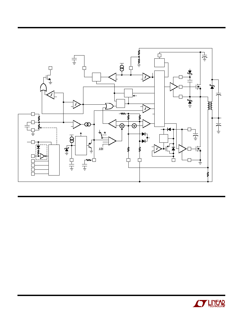
FU CTIO AL DIAGRA
U
U
W
OPERATIO
U
(Refer to Functional Diagram)
Main Control Loop
The LTC1736 uses a constant frequency, current mode
step-down architecture. During normal operation, the
top MOSFET is turned on each cycle when the oscillator
sets the RS latch, and turned off when the main current
comparator I1 resets the RS latch. The peak inductor
current at which I1 resets the RS latch is controlled by the
voltage on Pin I
TH
, which is the output of the error
amplifier EA. Pin V
OSENSE
, described in the Pin Functions,
allows EA to receive an output feedback voltage V
FB
from
the internal resistive divider. When the load current
increases, it causes a slight decrease in V
FB
relative to the
0.8V reference, which in turn causes the I
TH
voltage to
increase until the average inductor current matches the
new load current. While the top MOSFET is off, the
bottom MOSFET is turned on until either the inductor
current starts to reverse, as indicated by current com-
parator I2, or the beginning of the next cycle.
The top MOSFET driver is powered from a floating
bootstrap capacitor C
B
. This capacitor is normally re-
charged from INTV
CC
through an external Schottky diode
when the top MOSFET is turned off. As V
IN
decreases
towards V
OUT
, the converter will attempt to turn on the
top MOSFET continuously (`'dropout''). A dropout counter
detects this condition and forces the top MOSFET to turn
off for about 500ns every tenth cycle to recharge the
bootstrap capacitor.
SW
≠
+
+
≠
0.86V
0.74V
≠
+
0.55V
2.4V
0.8V
47pF
0.86V
I1
+
≠
I2
+
≠
EA
A
BURST
DISABLE
FC
OV
B
≠
+
4.8V
IREV
+
≠
+
≠
F
FC
S
R
Q
DROP
OUT
DET
0.8V
REF
SWITCH
LOGIC
SD
6V
RUN/SS
C
SS
R
C
V
FB
40k
1.2
µ
A
RUN
SOFT
START
+
OVER-
CURRENT
LATCH-OFF
SD
I
TH
C
C
0.17
µ
A
OSC
4(V
FB
)
BUFFERED
I
TH
SLOPE COMP
+
≠
≠
+
3mV
ICMP
R2
10k
R1
SGND
V
FB
V
OSENSE
2k
45k
BOT
TOP ON
FORCE BOT
45k
30k
30k
SENSE
+
SENSE
≠
SYNC
1.2V
0.8V
C
TOP
UVL
BOT
INTV
CC
5.2V
LDO
REG
V
IN
+
C
INTVCC
V
OUT
V
SEC
INTV
CC
BG
PGND
V
IN
V
IN
BOOST
TG
INTV
CC
C
B
D
B
D
1
C
OSC
+
C
IN
+
C
SEC
∑
∑
+
C
OUT
EXTV
CC
FCB
R4
R3
C
OSC
R
SENSE
1736 FD
1
PGOOD
6
9
10
5
VIDV
CC
VID4
INTV
CC
15
VID3 14
VID2 13
VID1 12
VID0 11
4
21
23
24
22
20
19
18
17
7
8
3
2
≠
+
VID
DECODER
16
g
m
=1.3m

9
LTC1736
OPERATIO
U
(Refer to Functional Diagram)
The main control loop is shut down by pulling Pin 2 (RUN/
SS) low. Releasing RUN/SS allows an internal 1.2
µ
A
current source to charge soft-start capacitor C
SS
. When
C
SS
reaches 1.5V, the main control loop is enabled with the
I
TH
voltage clamped at approximately 30% of its maximum
value. As C
SS
continues to charge, I
TH
is gradually re-
leased allowing normal operation to resume. If V
OUT
has
not reached 70% of its final value when C
SS
has charged
to 4.1V, latchoff can be invoked as described in the
Applications Information section.
The internal oscillator can be synchronized to an external
clock applied to the FCB pin and can lock to a frequency
between 90% and 130% of its nominal rate set by capaci-
tor C
OSC
.
An overvoltage comparator OV guards against transient
overshoots (> 7.5%) as well as other more serious condi-
tions that may overvoltage the output. In this case, the top
MOSFET is turned off and the bottom MOSFET is turned on
until the overvoltage condition is cleared.
Foldback current limiting for an output shorted to ground
is provided by amplifier A. As V
FB
drops below 0.6V, the
buffered I
TH
input to the current comparator is gradually
pulled down to a 0.86V clamp. This reduces peak inductor
current to about 1/4 of its maximum value.
Low Current Operation
The LTC1736 has three low current modes controlled by
the FCB pin. Burst Mode operation is selected when the
FCB pin is above 0.8V (typically tied to INTV
CC
). During
Burst Mode operation, if the error amplifier drives the I
TH
voltage below 0.86V, the buffered I
TH
input to the current
comparator will be clamped at 0.86V. The inductor current
peak is then held at approximately 20mV/R
SENSE
(about 1/
4 of maximum output current). If I
TH
then drops below
0.5V, the Burst Mode comparator B will turn off both
MOSFETs to maximize efficiency. The load current will be
supplied solely by the output capacitor until I
TH
rises
above the 60mV hysteresis of the comparator and switch-
ing is resumed. Burst Mode operation is disabled by
comparator F when the FCB pin is brought below 0.8V.
This forces continuous operation and can assist second-
ary winding regulation.
When the FCB pin is driven by an external oscillator, a low
noise cycle-skipping mode is invoked and the internal
oscillator is synchronized to the external clock by com-
parator C. In this mode the 25% minimum inductor
current clamp is removed, providing constant frequency
discontinuous operation over the widest possible output
current range. This constant frequency operation is not
quite as efficient as Burst Mode operation, but provides a
lower noise, constant frequency spectrum.
The FCB pin is tied to ground when forced continuous
operation is desired. This operation is the least efficient
mode, but is desirable in certain applications. The output
can source or sink current in this mode. When sinking
current while in forced continuous operation, current will
be forced back into the main power supply potentially
boosting the input supply to dangerous voltage levels--
BEWARE.
Foldback Current, Short-Circuit Detection
and Short-Circuit Latchoff
The RUN/SS capacitor, C
SS
, is used initially to limit the
inrush current of the switching regulator. After the con-
troller has been started and been given adequate time to
charge up the output capacitors and provide full load
current, C
SS
is used as a short-circuit time-out circuit. If
the output voltage falls to less than 70% of its nominal
output voltage, C
SS
begins discharging on the assumption
that the output is in an overcurrent and/or short-circuit
condition. If the condition lasts for a long enough period
as determined by the size of the C
SS
, the controller will be
shut down until the RUN/SS pin voltage is recycled. This
built-in latchoff can be overridden by providing a current
> 5
µ
A at a compliance of 5V to the RUN/SS pin. This
current shortens the soft-start period but also prevents net
discharge of C
SS
during an overcurrent and/or short-
circuit condition. Foldback current limiting is activated
when the output voltage falls below 70% of its nominal
level whether or not the short-circuit latchoff circuit is
enabled.

10
LTC1736
OPERATIO
U
(Refer to Functional Diagram)
INTV
CC
/EXTV
CC
Power
Power for the top and bottom MOSFET drivers and most
of the internal circuitry of the LTC1736 is derived from the
INTV
CC
pin. When the EXTV
CC
pin is left open, an internal
5.2V low dropout regulator supplies the INTV
CC
power
from V
IN
. If EXTV
CC
is raised above 4.7V, the internal
regulator is turned off and an internal switch connects
EXTV
CC
to INTV
CC
. This allows a high efficiency source,
such as the notebook main 5V system supply or a second-
ary output of the converter itself, to provide the INTV
CC
power. Voltages up to 7V can be applied to EXTV
CC
for
additional gate drive capability.
To provide clean start-up and to protect the MOSFETs,
undervoltage lockout is used to keep both MOSFETs off
until the input voltage is above 3.5V.
VID Control
Bits VID0 to VID4 are logic inputs setting the output volt-
age using an internal 5-bit DAC as a feedback resistive
voltage divider. The output voltage can be set in 50mV or
25mV increments from 0.925V to 2.0V according to
Table 1. Pins VID0 to VID4 are internally pulled up to
VIDV
CC
.
PGOOD
A window comparator monitors the output voltage and its
open-drain output is pulled low when the divided down
output voltage is not within
±
7.5% of the reference voltage
of 0.8V.
R
mV
I
SENSE
MAX
=
50
C
OSC
Selection for Operating Frequency
and Synchronization
The choice of operating frequency and inductor value is a
trade-off between efficiency and component size. Low
frequency operation improves efficiency by reducing
MOSFET switching losses, both gate charge loss and
transition loss. However, lower frequency operation re-
quires more inductance for a given amount of ripple
current.
The LTC1736 uses a constant-frequency architecture with
the frequency determined by an external oscillator capaci-
tor C
OSC
. Each time the topside MOSFET turns on, the
voltage on C
OSC
is reset to ground. During the on-time
C
OSC
is charged by a fixed current. When the voltage on the
capacitor reaches 1.19V, C
OSC
is reset to ground. The
process then repeats.
The value of C
OSC
is calculated from the desired operating
frequency assuming no external clock input on the FCB
pin:
APPLICATIO S I FOR ATIO
W
U
U
U
The basic LTC1736 application circuit is shown in
Figure 1 on the first page of this data sheet. External
component selection is driven by the load requirement
and begins with the selection of R
SENSE
. Once R
SENSE
is
known, C
OSC
and L can be chosen. Next, the power MOS-
FETs and D1 are selected. The operating frequency and the
inductor are chosen based largely on the desired amount
of ripple current. Finally, C
IN
is selected for its ability to
handle the large RMS current into the converter and C
OUT
is chosen with low enough ESR to meet the output voltage
ripple and transient specifications. The circuit shown in
Figure 1 can be configured for operation up to an input
voltage of 28V (limited by the external MOSFETs).
R
SENSE
Selection For Output Current
R
SENSE
is chosen based on the required output current.
The LTC1736 current comparator has a maximum thresh-
old of 75mV/R
SENSE
and an input common mode range of
SGND to 1.1(INTV
CC
). The current comparator threshold
sets the peak of the inductor current, yielding a maximum
average output current I
MAX
equal to the peak value less
half the peak-to-peak ripple current,
I
L
.
Allowing a margin for variations in the LTC1736 and
external component values yields:
11
LTC1736
APPLICATIO S I FOR ATIO
W
U
U
U
C
pF
Frequency
OSC
(
)
. (
)
≠
=
1 61 10
11
7
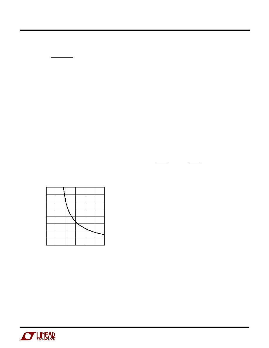
A graph for selecting C
OSC
versus frequency is given in
Figure 2. The maximum recommended switching fre-
quency is 550kHz .
The internal oscillator runs at its nominal frequency (f
O
)
when the FCB pin is pulled high to INTV
CC
or connected to
ground. Clocking the FCB pin above and below 0.8V will
cause the internal oscillator to lock to an external clock
signal with a frequency between 0.9f
O
and 1.3f
O
. The clock
high level must exceed 1.3V for at least 0.3
µ
s, and the
clock low level must be less than 0.3V for at least 0.3
µ
s.
The top MOSFET turn-on will synchronize with the rising
edge of the external clock.
Attempting to synchronize to too high an external fre-
quency (above 1.3f
O
) can result in inadequate slope com-
pensation and possible loop instability at high duty cycles.
If this condition exists simply lower the value of C
OSC
so
f
EXT
= f
O
according to Figure 2.
cycles to recharge the bootstrap capacitor. This minimizes
audible noise while maintaining reasonably high efficiency.
Inductor Value Calculation
The operating frequency and inductor selection are inter-
related in that higher operating frequencies allow the use
of smaller inductor and capacitor values. So why would
anyone ever choose to operate at lower frequencies with
larger components? The answer is efficiency. A higher
frequency generally results in lower efficiency because of
MOSFET gate-charge losses. In addition to this basic
trade-off, the effect of inductor value on ripple current and
low current operation must also be considered.
The inductor value has a direct effect on ripple current. The
inductor ripple current
I
L
decreases with higher induc-
tance or frequency and increases with higher V
IN
or V
OUT
:
I
f L
V
V
V
L
OUT
OUT
IN
=
1
1
( )( )
≠
Accepting larger values of
I
L
allows the use of low
inductances, but results in higher output voltage ripple
and greater core losses. A reasonable starting point for
setting ripple current is
I
L
= 0.3 to 0.4(I
MAX
). Remember,
the maximum
I
L
occurs at the maximum input voltage.
The inductor value also has an effect on low current
operation. The transition to low current operation begins
when the inductor current reaches zero while the bottom
MOSFET is on. Burst Mode operation begins when the
average inductor current required results in a peak current
below 25% of the current limit determined by R
SENSE
.
Lower inductor values (higher
I
L
) will cause this to occur
at higher load currents, which can cause a dip in efficiency
in the upper range of low current operation. In Burst Mode
operation, lower inductance values will cause the burst
frequency to decrease.
Inductor Core Selection
Once the value for L is known, the type of inductor must
be selected. High efficiency converters generally cannot
afford the core loss found in low cost powdered iron
cores, forcing the use of more expensive ferrite,
OPERATING FREQUENCY (kHz)
0
100
200
300
400
500
600
C
OSC
VALUE (pF)
1736 F02
100.0
87.5
75.0
62.5
50.0
37.5
25.0
12.5
0
When synchronized to an external clock, Burst Mode op-
eration is disabled but the inductor current is not allowed
to reverse. The 25% minimum inductor current clamp
present in Burst Mode operation is removed, providing
constant frequency discontinuous operation over the wid-
est possible output current range. In this mode the
synchronous MOSFET is forced on once every 10 clock
Figure 2. Timing Capacitor Value
12
LTC1736
APPLICATIO S I FOR ATIO
W
U
U
U
molypermalloy or Kool M
µ
Æ
cores. Actual core loss is
independent of core size for a fixed inductor value, but it
is very dependent on the inductance selected. As induc-
tance increases, core losses go down. Unfortunately,
increased inductance requires more turns of wire and
therefore copper losses will increase.
Ferrite designs have very low core loss and are preferred
at high switching frequencies, so design goals can con-
centrate on copper loss and preventing saturation. Ferrite
core material saturates "hard," which means that induc-
tance collapses abruptly when the peak design current is
exceeded. This results in an abrupt increase in inductor
ripple current and consequent output voltage ripple. Do
not allow the core to saturate!
Molypermalloy (from Magnetics, Inc.) is a very good, low
loss core material for toroids, but it is more expensive than
ferrite. A reasonable compromise from the same manu-
facturer is Kool M
µ
. Toroids are very space efficient,
especially when you can use several layers of wire. Be-
cause they generally lack a bobbin, mounting is more
difficult. However, designs for surface mount are available
that do not increase the height significantly.
Power MOSFET and D1 Selection
Two external power MOSFETs must be selected for use
with the LTC1736: An N-channel MOSFET for the top
(main) switch and an N-channel MOSFET for the bottom
(synchronous) switch.
The peak-to-peak gate drive levels are set by the INTV
CC
voltage. This voltage is typically 5.2V during start-up. (See
EXTV
CC
Pin Connection.) Consequently, logic-level thresh-
old MOSFETs must be used in most LTC1736 applica-
tions. The only exception is when low input voltage is
expected (V
IN
< 5V); then, sublogic level threshold
MOSFETs (V
GS(TH)
< 3V) should be used. Pay close
attention to the BV
DSS
specification for the MOSFETs as
well; most of the logic level MOSFETs are limited to 30V or
less.
Selection criteria for the power MOSFETs include the "ON"
resistance R
DS(ON)
, reverse transfer capacitance C
RSS
,
input voltage and maximum output current. When the
LTC1736 is operating in continuous mode the duty cycles
for the top and bottom MOSFETs are given by:
Main Switch Duty Cycle
V
V
Synchronous Switch Duty Cycle
V
V
V
OUT
IN
IN
OUT
IN
=
=
≠
The MOSFET power dissipations at maximum output
current are given by:
P
V
V
I
R
k V
I
C
f
P
V
V
V
I
R
MAIN
OUT
IN
MAX
DS ON
IN
MAX
RSS
SYNC
IN
OUT
IN
MAX
DS ON
=
( )
+
( )
+
( ) ( )( )( )
=
( )
+
( )
2
2
2
1
1
(
)
(
)
≠
where
is the temperature dependency of R
DS(ON)
and k
is a constant inversely related to the gate drive current.
Both MOSFETs have I
2
R losses while the topside
N-Channel equation includes an additional term for tran-
sition losses, which are highest at high input voltages. For
V
IN
< 20V the high current efficiency generally improves
with larger MOSFETs, while for V
IN
> 20V the transition
losses rapidly increase to the point that the use of a higher
R
DS(ON)
device with lower C
RSS
actually provides higher
efficiency. The synchronous MOSFET losses are greatest
at high input voltage or during a short circuit when the duty
cycle in this switch is nearly 100%.
The term (1 +
) is generally given for a MOSFET in the
form of a normalized R
DS(ON)
vs Temperature curve, but
= 0.005/
∞
C can be used as an approximation for low
voltage MOSFETs. C
RSS
is usually specified in the MOSFET
characteristics. The constant k = 1.7 can be used to
estimate the contributions of the two terms in the main
switch dissipation equation.
The Schottky diode D1 shown in Figure 1 conducts during
the dead-time between the conduction of the two power
MOSFETs. This prevents the body diode of the bottom
MOSFET from turning on and storing charge during the
dead-time, which could cost as much as 1% in efficiency.
A 3A Schottky is generally a good size for 10A to 12A
regulators due to the relatively small average current.
Kool M
µ
is a registered trademark of Magnetics, Inc.

13
LTC1736
APPLICATIO S I FOR ATIO
W
U
U
U
C
OUT
required ESR < 2.2 R
SENSE
C
OUT
> 1/(8fR
SENSE
)
The first condition relates to the ripple current into the ESR
of the output capacitance while the second term guaran-
tees that the output capacitance does not significantly
discharge during the operating frequency period due to
ripple current. The choice of using smaller output capaci-
tance increases the ripple voltage due to the discharging
term but can be compensated for by using capacitors of
very low ESR to maintain the ripple voltage at or below
50mV. The I
TH
pin OPTI-LOOP compensation compo-
nents can be optimized to provide stable, high perfor-
mance transient response regardless of the output capaci-
tors selected.
The selection of output capacitors for CPU or other appli-
cations with large load current transients is primarily
determined by the voltage tolerance specifications of the
load. The resistive component of the capacitor, ESR,
multiplied by the load current change plus any output
voltage ripple must be within the voltage tolerance of the
load (CPU).
The required ESR due to a load current step is:
R
ESR
<
V/
I
where
I is the change in current from full load to zero load
(or minimum load) and
V is the allowed voltage deviation
(not including any droop due to finite capacitance).
The amount of capacitance needed is determined by the
maximum energy stored in the inductor. The capacitance
must be sufficient to absorb the change in inductor current
when a high current to low current transition occurs. The
opposite load current transition is generally determined by
the control loop OPTI-LOOP components, so make sure
not to over compensate and slow down the response. The
minimum capacitance to assure the inductors' energy is
adequately absorbed is:
C
L
I
V V
OUT
OUT
>
( )
( )
2
2
where
I is the change in load current.
Larger diodes can result in additional transition losses due
to their larger junction capacitance. The diode may be
omitted if the efficiency loss can be tolerated.
C
IN
Selection
In continuous mode, the source current of the top
N-channel MOSFET is a square wave of duty cycle V
OUT
/
V
IN
. To prevent large voltage transients, a low ESR input
capacitor sized for the maximum RMS current must be
used. The maximum RMS capacitor current is given by:
I
I
V
V
V
V
RMS
O MAX
OUT
IN
IN
OUT
(
)
/
≠ 1
1 2
This formula has a maximum at V
IN
= 2V
OUT
, where I
RMS
= I
OUT
/2. This simple worst-case condition is commonly
used for design because even significant deviations do not
offer much relief. Note that capacitor manufacturers'
ripple current ratings are often based on only 2000 hours
of life. This makes it advisable to further derate the
capacitor, or to choose a capacitor rated at a higher
temperature than required. Several capacitors may also be
paralleled to meet size or height requirements in the
design. Always consult the manufacturer if there is any
question.
C
OUT
Selection
The selection of C
OUT
is primarily determined by the
effective series resistance (ESR) to minimize voltage ripple.
The output ripple (
V
OUT
) in continuous mode is deter-
mined by:
V
I ESR
fC
OUT
L
OUT
+
1
8
Where f = operating frequency, C
OUT
= output capaci-
tance, and
I
L
= ripple current in the inductor. The output
ripple is highest at maximum input voltage since
I
L
increases with input voltage. Typically, once the ESR
requirement for C
OUT
has been met, the RMS current
rating generally far exceeds the I
RIPPLE(P-P)
requirement.
With
I
L
= 0.3I
OUT(MAX)
the output ripple will be less than
50mV at max V
IN
assuming:

14
LTC1736
APPLICATIO S I FOR ATIO
W
U
U
U
Manufacturers such as Nichicon, United Chemicon and
Sanyo can be considered for high performance through-
hole capacitors. The OS-CON semiconductor dielectric
capacitor available from Sanyo has the lowest (ESR)(size)
product of any aluminum electrolytic at a somewhat
higher price. An additional ceramic capacitor in parallel
with OS-CON capacitors is recommended to reduce the
inductance effects.
In surface mount applications multiple capacitors may
need to be used in parallel to meet the ESR, RMS current
handling, and load step requirements of the application.
Aluminum electrolytic, dry tantalum and special polymer
capacitors are available in surface mount packages. Spe-
cial polymer surface mount capacitors offer very low ESR
but have much lower capacitive density per unit volume
than other capacitor types. These capacitors offer a very
cost-effective output capacitor solution and are an ideal
choice when combined with a controller having high loop
bandwidth. Tantalum capacitors offer the highest capaci-
tance density and are often used as output capacitors for
switching regulators having controlled soft-start. Several
excellent surge-tested choices are the AVX TPS, AVX
TPSV or the KEMET T510 series of surface mount
tantalums, available in case heights ranging from 2mm to
4mm. Aluminum electrolytic capacitors can be used in
cost-driven applications providing that consideration is
given to ripple current ratings, temperature and long-term
reliability. A typical application will require several to many
aluminum electrolytic capacitors in parallel. A combina-
tion of the above mentioned capacitors will often result in
maximizing performance and minimizing overall cost.
Other capacitor types include Nichicon PL series, NEC
Neocap, Panasonic SP and Sprague 595D series. Consult
manufacturers for other specific recommendations.
Like all components, capacitors are not ideal. Each ca-
pacitor has its own benefits and limitations. Combina-
tions of different capacitor types have proven to be a very
cost effective solution. Remember also to include high
frequency decoupling capacitors. They should be placed
as close as possible to the power pins of the load. Any
inductance present in the circuit board traces negates
their usefulness.
INTV
CC
Regulator
An internal P-channel low dropout regulator produces the
5.2V supply that powers the drivers and internal circuitry
within the LTC1736. The INTV
CC
pin can supply a maxi-
mum RMS current of 50mA and must be bypassed to
ground with a minimum of 4.7
µ
F tantalum, 10
µ
F special
polymer or low ESR type electrolytic capacitor. Good
bypassing is required to supply the high transient currents
required by the MOSFET gate drivers.
Higher input voltage applications in which large MOSFETs
are being driven at high frequencies may cause the
maximum junction temperature rating for the LTC1736 to
be exceeded. The system supply current is normally
dominated by the gate charge current. Additional loading
of INTV
CC
also needs to be taken into account for the
power dissipation calculations. The total INTV
CC
current
can be supplied by either the 5.2V internal linear regulator
or by the EXTV
CC
input pin. When the voltage applied to
the EXTV
CC
pin is less than 4.7V, all of the INTV
CC
current
is supplied by the internal 5.2V linear regulator. Power
dissipation for the IC in this case is highest: (V
IN
)(I
INTVCC
),
and overall efficiency is lowered. The gate charge is
dependent on operating frequency as discussed in the
Efficiency Considerations section. The junction tempera-
ture can be estimated by using the equations given in
Note 2 of the Electrical Characteristics. For example, the
LTC1736G is limited to less than 17mA from a 30V supply
when not using the EXTV
CC
pin as follows:
T
J
= 70
∞
C + (17mA)(30V)(110
∞
C/W) = 126
∞
C
Use of the EXTV
CC
input pin reduces the junction tempera-
ture to:
T
J
= 70
∞
C + (17mA)(5V)(110
∞
C/W) = 79
∞
C
To prevent maximum junction temperature from being
exceeded, the input supply current must be checked
operating in continuous mode at maximum V
IN
.
EXTV
CC
Connection
The LTC1736 contains an internal P-channel MOSFET
switch connected between the EXTV
CC
and INTV
CC
pins.
Whenever the EXTV
CC
pin is above 4.7V the internal 5.2V

15
LTC1736
APPLICATIO S I FOR ATIO
W
U
U
U
regulator shuts off, the switch closes and INTV
CC
power is
supplied via EXTV
CC
until EXTV
CC
drops below 4.5V. This
allows the MOSFET gate drive and control power to be
derived from the output or other external source during
normal operation. When the output is out of regulation
(start-up, short circuit) power is supplied from the internal
regulator. Do not apply greater than 7V to the EXTV
CC
pin
and ensure that EXTV
CC
< V
IN
.
Significant efficiency gains can be realized by powering
INTV
CC
from the output, since the V
IN
current resulting
from the driver and control currents will be scaled by a
factor of (Duty Cycle)/(Efficiency). For 5V regulators this
simply means connecting the EXTV
CC
pin directly to V
OUT
.
However, for VID programmed regulators and other lower
voltage regulators, additional circuitry is required to de-
rive INTV
CC
power from the output.
The following list summarizes the three possible connec-
tions for EXTV
CC:
1. EXTV
CC
Left Open (or Grounded). This will cause INTV
CC
to be powered from the internal 5.2V regulator resulting
in a low current efficiency penalty of up to 10% at high
input voltages.
2. EXTV
CC
Connected to an External Supply (this option is
the most likely used). If an external supply is available
in the 5V to 7V range, such as notebook main 5V
system power, it may be used to power EXTV
CC
provid-
ing it is compatible with the MOSFET gate drive
requirements. This is the typical case as the 5V power
is almost always present and is derived by another high
efficiency regulator.
3. EXTV
CC
Connected to an Output-Derived Boost Net-
work. For this low output voltage regulator, efficiency
gains can still be realized by connecting EXTV
CC
to an
output-derived voltage that has been boosted to greater
than 4.7V. This can be done with either the inductive
boost winding or the capacitive charge pump circuits.
Refer to the LTC1735 data sheet for details. The charge
pump has the advantage of simple magnetics.
Output Voltage Programming
The output voltage is digitally set to levels between 0.925V
and 2.00V using the voltage identification (VID) inputs
VID0 to VID4. The internal 5-bit DAC configured as a
precision resistive voltage divider sets the output voltage
in 50mV or 25mV increments according to Table 1.
The VID codes (00000-11110) are engineered to be com-
patible with Intel Mobile Pentium II
and Pentium III pro-
cessor specifications for output voltages from 0.925V to
2.00V.
The LSB (VID0) represents 50mV increments in the upper
voltage range (1.30V to 2.00V) and 25mV increments in
the lower voltage range (0.925V to 1.275V). The MSB is
VID4. When all bits are low, or grounded, the output
voltage is 2.00V.
Between the V
FB
pin and ground is a variable resistor, R1,
whose value is controlled by the five input pins (VID0 to
VID4). Another resistor, R2, between the V
OSENSE
and the
V
FB
pins completes the resistive divider. The output volt-
age is thus set by the ratio of (R1 + R2) to R1.
The LTC1736 has remote sense capability. The top of the
internal resistive divider is connected to V
OSENSE
, and it is
referenced to the SGND pin. This allows a kelvin connec-
tion for remotely sensing the output voltage directly across
the load, eliminating any PC board trace resistance errors.
Each VID digital input is pulled up by a 40k resistor in
series with a diode from VIDV
CC
. Therefore, it must be
grounded to get a digital low input, and can be either
floated or connected to VIDV
CC
to get a digital high input.
The series diode is used to prevent the digital inputs from
being damaged or clamped if they are driven higher than
VIDV
CC
. The digital inputs accept CMOS voltage levels.
VIDV
CC
is the supply voltage for the VID section. It is
normally connected to INTV
CC
but can be driven from
other sources such as a 3.3V supply. If it is driven from
another source, that source MUST be in the range of 2.7V
to 5.5V and MUST be alive prior to enabling the LTC1736.
16
LTC1736
APPLICATIO S I FOR ATIO
W
U
U
U
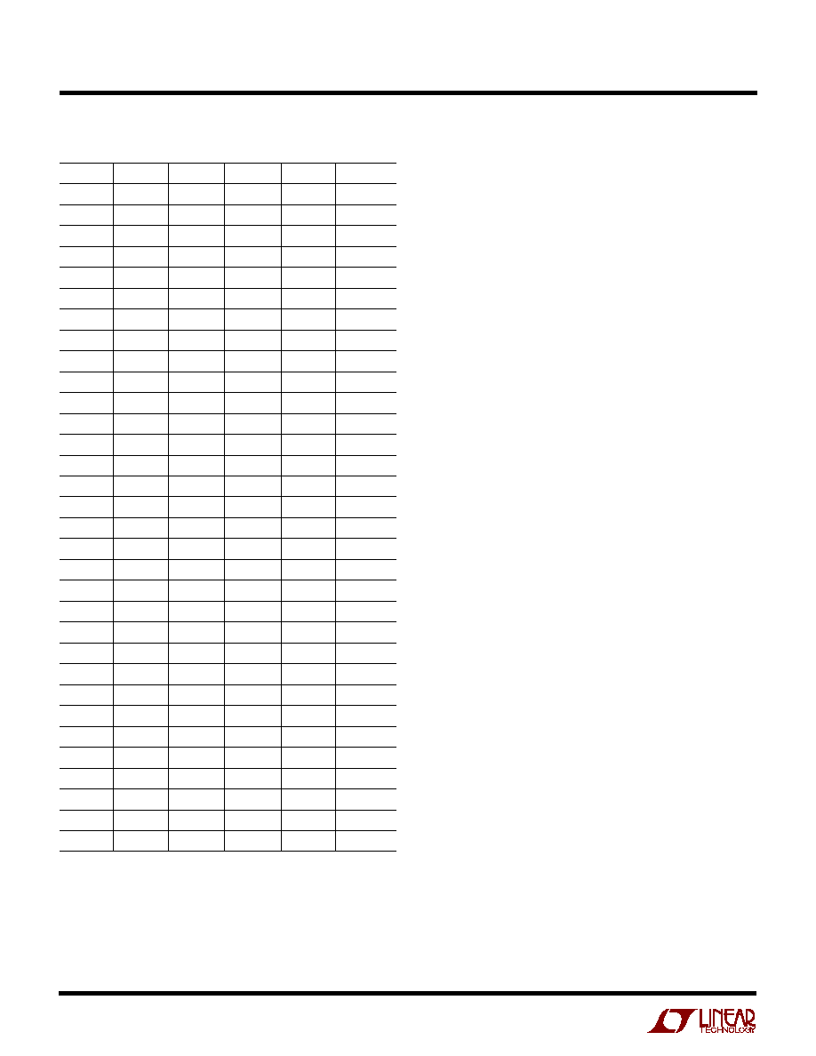
Table 1. VID Output Voltage Programming
VID4
VID3
VID2
VID1
VID0
V
OUT
(V)
0
0
0
0
0
2.000V
0
0
0
0
1
1.950V
0
0
0
1
0
1.900V
0
0
0
1
1
1.850V
0
0
1
0
0
1.800V
0
0
1
0
1
1.750V
0
0
1
1
0
1.700V
0
0
1
1
1
1.650V
0
1
0
0
0
1.600V
0
1
0
0
1
1.550V
0
1
0
1
0
1.500V
0
1
0
1
1
1.450V
0
1
1
0
0
1.400V
0
1
1
0
1
1.350V
0
1
1
1
0
1.300V
0
1
1
1
1
*
1
0
0
0
0
1.275V
1
0
0
0
1
1.250V
1
0
0
1
0
1.225V
1
0
0
1
1
1.200V
1
0
1
0
0
1.175V
1
0
1
0
1
1.150V
1
0
1
1
0
1.125V
1
0
1
1
1
1.100V
1
1
0
0
0
1.075V
1
1
0
0
1
1.050V
1
1
0
1
0
1.025V
1
1
0
1
1
1.000V
1
1
1
0
0
0.975V
1
1
1
0
1
0.950V
1
1
1
1
0
0.925V
1
1
1
1
1
**
Note: *, ** represents codes without a defined output voltage as specified in
Intel specifications. The LTC1736 interprets these codes as valid inputs and
produces output voltages as follows: [01111] = 1.250V, [11111] = 0.900V.
Topside MOSFET Driver Supply (C
B
, D
B
)
An external bootstrap capacitor C
B
connected to the BOOST
pin supplies the gate drive voltage for the topside MOSFET.
Capacitor C
B
in the Functional Diagram is charged though
external diode D
B
from INTV
CC
when the SW pin is low.
Note that the voltage across C
B
is about a diode drop below
INTV
CC
. When the topside MOSFET is to be turned on, the
driver places the C
B
voltage across the gate-source of the
MOSFET. This enhances the MOSFET and turns on the
topside switch. The switch node voltage SW rises to V
IN
and the BOOST pin rises to V
IN
+ INTV
CC
. The value of the
boost capacitor C
B
needs to be 100 times greater than the
total input capacitance of the topside MOSFET. In most
applications 0.1
µ
F to 0.33
µ
F is adequate. The reverse
breakdown on D
B
must be greater than V
IN(MAX) .
When adjusting the gate drive level, the final arbiter is the
total input current for the regulator. If you make a change
and the input current decreases, then you improve the
efficiency. If there is no change in input current, then there
is no change in efficiency.
SENSE
+
/SENSE
≠
Pins
The common mode input range of the current comparator
is from 0V to 1.1(INTV
CC
). Continuous linear operation is
guaranteed throughout this range allowing output volt-
ages anywhere from 0.8V to 7V (although the VID control
pins only program a 0.925V to 2.00V output range). A
differential NPN input stage is used and is biased with
internal resistors from an internal 2.4V source as shown
in the Functional Diagram. This causes current to flow out
of both sense pins to the main output. This forces a
minimum load current which is sunk by the internal
resistive divider resistors R1 and R2. The maximum
current flowing out of the sense pins is:
I
SENSE +
+ I
SENSE ≠
= (2.4V ≠ V
OUT
)/24k
Remember to take this current into account if resistance is
placed in series with the sense pins for filtering.
17
LTC1736
APPLICATIO S I FOR ATIO
W
U
U
U
Soft-Start/Run Function
The RUN/SS pin is a multipurpose pin that provides a soft-
start function and a means to shut down the LTC1736.
Soft-start reduces surge currents from V
IN
by gradually
increasing the controller's current limit I
TH(MAX)
. This pin
can also be used for power supply sequencing.
Pulling the RUN/SS pin below 1.5V puts the LTC1736 into
a low quiescent current shutdown (I
Q
< 25
µ
A). This pin can
be driven directly from logic as shown in Figure 3. Releas-
ing the RUN/SS pin allows an internal 1.2
µ
A current
source to charge up the external soft-start capacitor C
SS.
If RUN/SS has been pulled all the way to ground there is
a delay before starting of approximately:
t
V
A
C
s
F C
DELAY
SS
SS
=
µ
=
µ
(
)
1 5
1 2
1 25
.
.
.
/
When the voltage on RUN/SS reaches 1.5V the LTC1736
begins operating with a current limit at approximately
25mV/R
SENSE
. As the voltage on RUN/SS increases from
1.5V to 3.0V, the internal current limit is increased from
25mV/R
SENSE
to 75mV/R
SENSE
. The output current limit
ramps up slowly, taking an additional 1.25s/
µ
F to reach
full current. The output current thus ramps up slowly
reducing the starting surge current required from the input
power supply.
Diode D1 in Figure 3 reduces the start delay while allowing
C
SS
to charge up slowly for the soft-start function. This
diode and C
SS
can be deleted if soft-start is not needed.
The RUN/SS pin has an internal 6V zener clamp (See
Functional Diagram).
Fault Conditions: Overcurrent Latchoff
The RUN/SS pin also provides the ability to shut off the
controller and latchoff when an overcurrent condition is
detected. The RUN/SS capacitor C
SS
is used initially to
turn on and limit the inrush current of the controller. After
the controller has been started and given adequate time to
charge up the output capacitor and provide full load
current, C
SS
is used as a short-circuit timer. If the output
voltage falls to less than 70% of its nominal output voltage
after C
SS
reaches 4.1V, the assumption is made that the
output is in a severe overcurrent and/or short-circuit
condition and C
SS
begins discharging. If the condition
lasts for a long enough period as determined by the size of
C
SS
, the controller will be shut down until the RUN/SS pin
voltage is recycled.
This built-in latchoff can be overridden by providing a
current > 5
µ
A at a compliance of 5V to the RUN/SS pin as
shown in Figure 4. This current shortens the soft-start
period but also prevents net discharge of the RUN/SS
capacitor during a severe overcurrent and/or short-circuit
condition. When deriving the 5
µ
A current from V
IN
as in
Figure 4a, current latchoff is always defeated. A diode
connecting this pull-up resistor to INTV
CC
, as in Figure 4b,
eliminates any extra supply current during controller shut-
down while eliminating the INTV
CC
loading from prevent-
ing controller start-up. If the voltage on C
SS
does not exceed
4.1V, the overcurrent latch is not armed and the function
is disabled.
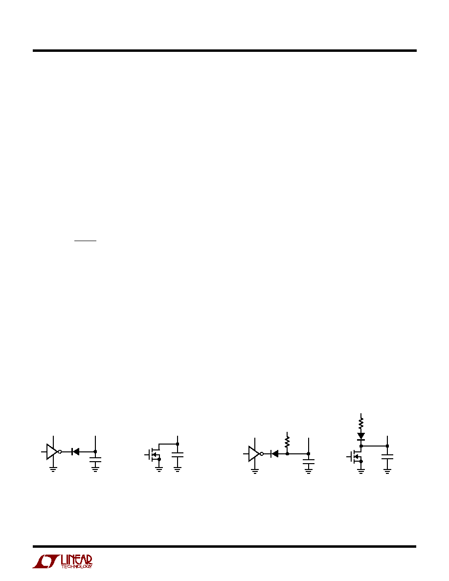
Figure 3. RUN/SS Pin Interfacing
3.3V OR 5V
RUN/SS
D1
RUN/SS
(a)
(b)
C
SS
C
SS
1736 F03
3.3V OR 5V
RUN/SS
V
IN
INTV
CC
RUN/SS
D1
(a)
(b)
D1
C
SS
R
SS
C
SS
R
SS
1736 F04
Figure 4. RUN/SS Pin Interfacing with Latchoff Defeated

18
LTC1736
APPLICATIO S I FOR ATIO
W
U
U
U
Why should you defeat overcurrent latchoff? During the
prototyping stage of a design, there may be a problem with
noise pickup or poor layout causing the protection circuit
to latch off. Defeating this feature will easily allow trouble-
shooting of the circuit and PC layout. The internal short-
circuit and foldback current limiting still remains active,
thereby protecting the power supply system from failure.
After the design is complete, a decision can be made
whether to enable the latchoff feature.
The value of the soft-start capacitor C
SS
will need to be
scaled with output voltage, output capacitance and load
current characteristics. The minimum soft-start capaci-
tance is given by:
C
SS
> (C
OUT
)(V
OUT
)(10
≠ 4
)(R
SENSE
)
The minimum recommended soft-start capacitor of C
SS
=
0.1
µ
F will be sufficient for most applications.
Fault Conditions: Current Limit and Current Foldback
The LTC1736 current comparator has a maximum sense
voltage of 75mV resulting in a maximum MOSFET current
of 75mV/R
SENSE
.
The LTC1736 includes current foldback to help further
limit load current when the output is shorted to ground.
The foldback circuit is active even when the overload
shutdown latch described above is defeated. If the output
falls by more than half, then the maximum sense voltage
is progressively lowered from 75mV to 30mV. Under
short-circuit conditions with very low duty cycle, the
LTC1736 will begin cycle skipping in order to limit the
short-circuit current. In this situation the bottom MOSFET
will be conducting the peak current. The short-circuit
ripple current is determined by the minimum on-time
t
ON(MIN)
of the LTC1736 (less than 200ns), the input
voltage, and inductor value:
I
L(SC)
= t
ON(MIN)
V
IN
/L.
The resulting short circuit current is:
I
mV
R
I
SC
SENSE
L SC
=
+
30
1
2
(
)
The current foldback function is always active and is not
effected by the current latchoff function.
Fault Conditions: Output Overvoltage Protection
(Crowbar)
The output overvoltage crowbar is designed to blow a
system fuse in the input lead when the output of the
regulator rises much higher than nominal levels. This
condition causes huge currents to flow, much greater than
in normal operation. This feature is designed to protect
against a shorted top MOSFET; it does not protect against
a failure of the controller itself.
The comparator (OV in the Functional Diagram) detects
overvoltage faults greater than 7.5% above the nominal
output voltage. When this condition is sensed, the top
MOSFET is turned off and the bottom MOSFET is forced
on. The bottom MOSFET remains on continuously for as
long as the OV condition persists; if V
OUT
returns to a safe
level, normal operation automatically resumes. Note that
VID controlled output voltage decreases may cause the
overvoltage protection to be momentarily activated. This
will not cause permanent latchoff nor will it disrupt the
desired voltage change.
With soft-latch overvoltage protection, dynamic VID code
changes are allowed and the overvoltage protection tracks
the new VID code, always protecting the load (CPU). If
dynamic VID code changes are anticipated and the mini-
mum load current is light, it may be necessary to either
force continuous operation by pulling FCB low during the
transition to maximize current sinking capability or con-
nect PGOOD to FCB to automatically force continuous
operation during VID transitions.
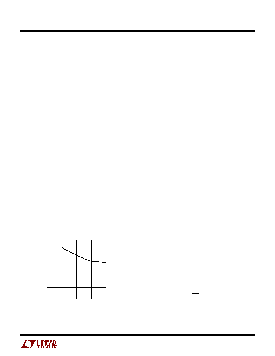
19
LTC1736
Minimum On-Time Considerations
Minimum on-time t
ON(MIN)
is the smallest amount of time
that the LTC1736 is capable of turning the top MOSFET on
and off again. It is determined by internal timing delays and
the gate charge required to turn on the top MOSFET. Low
duty cycle applications may approach this minimum on-
time limit and care should be taken to ensure that:
t
V
V f
ON MIN
OUT
IN
(
)
( )
<
If the duty cycle falls below what can be accommodated by
the minimum on-time, the LTC1736 will begin to skip
cycles. The output voltage will continue to be regulated,
but the ripple current and voltage will increase.
The minimum on-time for the LTC1736 in a properly
configured application is generally less than 200ns. How-
ever, as the peak sense voltage decreases, the minimum
on-time gradually increases as shown in Figure 5. This is
of particular concern in forced continuous applications
with low ripple current at light loads. If the duty cycle drops
below the minimum on-time limit in this situation, a
significant amount of cycle skipping can occur with corre-
spondingly larger current and voltage ripple.
If an application can operate close to the minimum on-
time limit, an inductor must be chosen that is low enough
in value to provide sufficient ripple amplitude to meet the
minimum on-time requirement.
As a general rule keep the
APPLICATIO S I FOR ATIO
W
U
U
U
inductor ripple current equal or greater than 30% of
I
OUT(MAX)
at V
IN(MAX)
.
FCB Pin Operation
When the DC voltage on the FCB pin drops below its 0.8V
threshold, continuous mode operation is forced. In this
case, the top and bottom MOSFETs continue to be driven
synchronously regardless of the load on the main output.
Burst Mode operation is disabled and current reversal is
allowed in the inductor.
In addition to providing a logic input to force continuous
synchronous operation and external synchronization, the
FCB pin provides a means to regulate a flyback winding
output. During continuous mode, current flows continu-
ously in the transformer primary. The secondary winding(s)
draw current only when the bottom synchronous switch is
on. When primary load currents are low and/or the
V
IN
/V
OUT
ratio is low, the synchronous switch may not be
on for a sufficient amount of time to transfer power from
the output capacitor to the secondary load. Forced con-
tinuous operation will support secondary windings pro-
vided there is sufficient synchronous switch duty factor.
Thus, the FCB input pin removes the requirement that
power must be drawn from the inductor primary in order
to extract power from the auxiliary windings. With the loop
in continuous mode, the auxiliary output may nominally be
loaded without regard to the primary output load.
The secondary output voltage V
SEC
is normally set as
shown in the Functional Diagram by the turns ratio N of the
transformer:
V
SEC
(N + 1) V
OUT
However, if the controller goes into Burst Mode operation
and halts switching due to a light primary load current,
then V
SEC
will droop. An external resistive divider from
V
SEC
to the FCB pin sets a minimum voltage V
SEC(MIN)
:
V
V
R
R
SEC MIN
(
)
.
+
0 8
1
4
3
If V
SEC
drops below this level, the FCB voltage forces
continuous switching operation until V
SEC
is again above
its minimum.
I
L
/I
OUT(MAX)
(%)
0
MINIMUM ON-TIME (ns)
100
150
40
1736 F05
50
0
10
20
30
250
200
Figure 5. Minimum On-Time vs
I
L

20
LTC1736
In order to prevent erratic operation if no external connec-
tions are made to the FCB pin, the FCB pin has a 0.17
µ
A
internal current source pulling the pin high. Remember to
include this current when choosing resistor values R3 and
R4.
The internal LTC1736 oscillator can be synchronized to an
external oscillator by clocking the FCB pin with a signal
above 1.5V
P-P
. When synchronized to an external fre-
quency, Burst Mode operation is disabled, but cycle skip-
ping is allowed at low load currents since current reversal
is inhibited. The bottom gate will come on every 10 clock
cycles to assure the boostrap cap, C
B
, is kept refreshed.
The rising edge of an external clock applied to the FCB pin
starts a new cycle.
The range of synchronization is from 0.9f
O
to 1.3f
O
, with
f
O
set by C
OSC
. Attempting to synchronize to a higher
frequency than 1.3f
O
can result in inadequate slope
comensation and cause loop instability with high duty
cycles. If loop instability is observed while synchronized,
additional slope compensation can be obtained by simply
decreasing C
OSC
.
The following table summarizes the possible states avail-
able on the FCB pin:
Table 2
FCB Pin
Condition
DC Voltage: 0V to 0.7V
Burst Disabled/Forced Continuous
Current Reversal Enabled
DC Voltage: > 0.9V
Burst Mode Operation, No Current Reversal
Feedback Resistors
Regulating a Secondary Winding
Ext Clock: (0V to V
FCBSYNC
)
Burst Mode Operation Disabled
(V
FCBSYNC
1.5V) No Current Reversal
Efficiency Considerations
The percent efficiency of a switching regulator is equal to
the output power divided by the input power times 100%.
It is often useful to analyze individual losses to determine
what is limiting the efficiency and which change would
produce the most improvement. Percent efficiency can be
expressed as:
%Efficiency = 100% - (L1 + L2 + L3 + ...)
APPLICATIO S I FOR ATIO
W
U
U
U
where L1, L2, etc., are the individual losses as a percent-
age of input power.
Although all dissipative elements in the circuit produce
losses, four main sources usually account for most of the
losses in LTC1736 circuits: 1) LTC1736 V
IN
current, 2)
INTV
CC
current, 3) I
2
R losses, 4) Topside MOSFET transi-
tion losses.
1. The V
IN
current is the DC supply current given in the
electrical characteristics which excludes MOSFET driver
and control currents. V
IN
current results in a small
(< 0.1%) loss that increases with V
IN
.
2. INTV
CC
current is the sum of the MOSFET driver and
control currents. The MOSFET driver current results
from switching the gate capacitance of the power
MOSFETs. Each time a MOSFET gate is switched from
low to high to low again, a packet of charge dQ moves
from INTV
CC
to ground. The resulting dQ/dt is a current
out of INTV
CC
that is typically much larger than the
control circuit current. In continuous mode, I
GATECHG
=
f(Q
T
+ Q
B
), where Q
T
and Q
B
are the gate charges of the
topside and bottom-side MOSFETs.
Supplying INTV
CC
power through the EXTV
CC
switch
input from an output-derived or other high efficiency
source will scale the V
IN
current required for the driver
and control circuits by a factor of (Duty Cycle)/(Effi-
ciency). For example, in a 15V to 1.8V application, 10mA
of INTV
CC
current results in approximately 1.2mA of V
IN
current. This reduces the low current loss from 10% or
more (if the driver was powered directly from V
IN
) to only
a few percent.
3. I
2
R Losses are predicted from the DC resistances of the
MOSFETs, inductor and current shunt. In continuous
mode the average output current flows through L and
R
SENSE
, but is "chopped" between the topside main
MOSFET and the synchronous MOSFET. If the two
MOSFETs have approximately the same R
DS(ON)
, then
the resistance of one MOSFET can simply be summed
with the resistances of L and R
SENSE
to obtain I
2
R
losses. For example, if each R
DS(ON)
= 0.02
, R
L
=
0.03
, and R
SENSE
= 0.01
, then the total resistance is

21
LTC1736
APPLICATIO S I FOR ATIO
W
U
U
U
0.06
. This results in losses ranging from 3% to 17%
as the output current increases from 1A to 5A for a 1.8V
output, or 4% to 20% for a 1.5V output. Efficiency
varies as the inverse square of V
OUT
for the same
external components and power level. I
2
R losses cause
the efficiency to drop at high output currents.
4. Transition losses apply only to the topside MOSFET(s),
and only become significant when operating at high
input voltages (typically 12V or greater). Transition
losses can be estimated from:
Transition Loss = (1.7)(V
IN
2
)(I
O(MAX)
)(C
RSS
)(f)
Other "hidden" losses such as copper trace and internal
battery resistances can account for an additional 5% to
10% efficiency degradation in portable systems. It is very
important to include these "system" level losses in the
design of a system. The internal battery and fuse resis-
tance losses can be minimized by making sure that C
IN
has
adequate charge storage and very low ESR at the switch-
ing frequency. A 25W supply will typically require a
minimum of 20
µ
F to 40
µ
F of capacitance having a maxi-
mum of 0.01
to 0.02
of ESR. Other losses including
Schottky conduction losses during dead-time and induc-
tor core losses generally account for less than 2% total
additional loss.
Checking Transient Response
The regulator loop response can be checked by looking at
the load current transient response. Switching regulators
take several cycles to respond to a step in DC (resistive)
load current. When a load step occurs, V
OUT
shifts by an
amount equal to
I
LOAD
(ESR), where ESR is the effective
series resistance of C
OUT
.
I
LOAD
also begins to charge or
discharge C
OUT
generating the feedback error signal that
forces the regulator to adapt to the current change and
return V
OUT
to its steady-state value. During this recovery
time V
OUT
can be monitored for excessive overshoot or
ringing, which would indicate a stability problem. OPTI-
LOOP compensation allows the transient response to be
optimized over a wide range of output capacitance and
ESR values. The availability of the I
TH
pin not only allows
optimization of control loop behavior but also provides a
DC coupled and AC filtered closed-loop response test
point. The DC step, rise time and settling at this test point
truly reflects the closed-loop response. Assuming a pre-
dominantly second order system, phase margin and/or
damping factor can be estimated using the percentage of
overshoot seen at this pin. The bandwidth can also be
estimated by examining the rise time at the pin. The I
TH
external components shown in the Figure 1 circuit will
provide an adequate starting point for most applications.
The I
TH
series R
C
-C
C
filter sets the dominant pole-zero
loop compensation. The values can be modified slightly
(from 0.5 to 2 times their suggested values) to optimize
transient response once the final PC layout is done and the
particular output capacitor type and value have been
determined. The output capacitors need to be selected
because the various types and values determine the loop
feedback factor gain and phase. An output current pulse of
20% to 100% of full-load current having a rise time of 1
µ
s
to 10
µ
s will produce output voltage and I
TH
pin waveforms
that will give a sense of the overall loop stability without
breaking the feedback loop. The initial output voltage step
may not be within the bandwidth of the feedback loop, so
the standard second-order overshoot/DC ratio cannot be
used determine phase margin. The gain of the loop will be
increased by increasing R
C
and the bandwidth of the loop
will be increased by decreasing C
C
. If R
C
is increased by the
same factor that C
C
is decreased, the zero frequency will
be kept the same, thereby keeping the phase the same in
the most critical frequency range of the feedback loop. The
output voltage settling behavior is related to the stability of
the closed-loop system and will demonstrate the actual
overall supply performance. For a detailed explanation of
optimizing the compensation components, including a
review of control loop theory, refer to Application Note 76.
Improve Transient Response and Reduce Output
Capacitance with Active Voltage Positioning
Fast load transient response, limited board space and low
cost are requirements of microprocessor power supplies.
Active voltage positioning improves transient response
and reduces the output capacitance required to power a
microprocessor where a typical load step can be from 0.2A

22
LTC1736
to 15A in 100ns or 15A to 0.2A in 100ns. The voltage at the
microprocessor must be held to about
±
0.1V of nominal
in spite of these load current steps. Since the control loop
cannot respond this fast, the output capacitors must
supply the load current until the control loop can respond.
Capacitor ESR and ESL primarily determine the amount of
droop or overshoot in the output voltage. Normally, sev-
eral capacitors in parallel are required to meet micropro-
cessor transient requirements.
Active voltage positioning is a form of deregulation. It
sets the output voltage high for light loads and low for
heavy loads. When load current suddenly increases, the
output voltage starts from a level higher than nominal so
the output voltage can droop more and stay within the
specified voltage range. When load current suddenly
decreases the output voltage starts at a level lower than
nominal so the output voltage can have more overshoot
and stay within the specified voltage range. Less output
capacitance is required when voltage positioning is used
because more voltage variation is allowed on the output
capacitors.
Active voltage positioning can be implemented using the
OPTI-LOOP architecture of the LTC1736 with two external
resistors. An input voltage offset is introduced when the
error amplifier has to drive a resistive load. This offset is
limited to
±
30mV at the input of the error amplifier. The
resulting change in output voltage is the product of input
offset and the feedback voltage divider ratio.
Figure 6 shows a CPU-core-voltage regulator with active
voltage positioning. Resistors R1 and R5 force the input
voltage offset that sets the output voltage according to the
load current level. To select values for R1 and R5, first
determine the amount of output deregulation allowed. The
actual specification for a typical microprocessor allows
the output to vary
±
0.112V. The LTC1736 output voltage
1
2
3
4
5
6
7
8
9
10
11
12
24
23
22
21
20
19
18
17
16
15
14
13
C
OSC
RUN/SS
I
TH
FCB
SGND
PGOOD
SENSE
≠
SENSE
+
V
FB
V
OSENSE
VID0
VID1
TG
BOOST
SW
V
IN
INTV
CC
BG
PGND
EXTV
CC
VIDV
CC
VID4
VID3
VID2
LTC1736
C5
1000pF
C6
47pF
VID0
VID1
VID2
VID3
VID4
VID
INPUT
C7 330pF
C3
100pF
C1 39pF
C4 100pF
C2
0.1
µ
F
POWER
GOOD
R2
100k
R5
100k
R4
100k
R3
680k
R1
27k
+
C10
1
µ
F
5V (OPTIONAL)
C18
1
µ
F
C12 TO C14
10
µ
F
35V
C11
4.7
µ
F
10V
D1
CMDSH-3
C8
0.1
µ
F
D2
MBRS340
C9
0.22
µ
F
M1
FDS6680A
L1
1
µ
H
R6
0.003
M2, M3
FDS6680A
◊
2
1736 F06
C15 TO C17
180
µ
F/4V
◊
4
V
OUT
0.9V TO 2V
15A
GND
GND
V
IN
7.5V TO 24V
+
C10, C18: TAIYO YUDEN JMK107BJ105
C11: KEMET T494A475M010AS
C12 TO C14: TAIYO YUDEN GMK325F106
C15 TO C17: PANASONIC EEFUE0G181R
D1: CENTRAL SEMI CMDSH-3
D2: MOTOROLA MBRS340
L1: PANASONIC ETQP6F1R0SA
M1 TO M3: FAIRCHILD FDS6680A
R6: IRC LRF2512-01-R003-J
U1: LINEAR TECHNOLOGY LTC1736CG
Figure 6. CPU-Core-Voltage Regulator with Active Voltage Positioning
APPLICATIO S I FOR ATIO
W
U
U
U
23
LTC1736
accuracy is
±
1%, so the output transient voltage cannot
exceed
±
0.097V. At V
OUT
= 1.5V, the maximum output
voltage change controlled by the I
TH
pin would be:
=
=
±
= ±
V
Input Offset V
V
V
V
mV
OSENSE
OUT
REF
∑
.
∑ .
.
0 03
1 5
0 8
56
With optimum resistor values at the I
TH
pin, the output
voltage will swing from 1.55V at minimum load to 1.44V
at full load. At this output voltage, active voltage position-
ing provides an additional 56mV to the allowable transient
voltage on the output capacitors, a 58% improvement
over the 97mV allowed without active voltage positioning.
The next step is to calculate the I
TH
pin voltage, V
ITH
, scale
factor. The V
ITH
scale factor reflects the I
TH
pin voltage
required for a given load current. V
ITH
controls the peak
sense resistor voltage, which represents the DC output
current plus one half of the peak-to-peak inductor current.
The no load to full load V
ITH
range is from 0.3V to 2.4V,
which controls the sense resistor voltage from 0V to the
V
SENSE(MAX)
voltage of 75mV. The calculated V
ITH
scale
factor with a 0.003
sense resistor is:
V
Scale Factor
V
Range Sense
sistor Value
V
V
V
V
V A
ITH
ITH
SENSE MAX
=
=
=
∑
Re
( .
≠ .
) ∑ .
.
.
/
(
)
2 4
0 3
0 003
0 075
0 084
V
ITH
at any load current is:
V
I
I
V
Scale Factor
V
Offset
ITH
OUT DC
L
ITH
ITH
=
+
+
(
)
∑
2
At full load current:
V
A
A
V A
V
V
ITH MAX
P P
(
)
∑ .
/
.
.
=
+
+
=
-
15
5
2
0 084
0 3
1 77
At minimum load current:
V
A
A
V A
V
V
ITH MIN
P P
(
)
.
∑ .
/
.
.
=
+
+
=
-
0 2
2
2
0 084
0 3
0 40
In this circuit, V
ITH
changes from 0.40V at light load to
1.77V at full load, a 1.37V change. Notice that
I
L
, the
peak-to-peak inductor current, changes from light load to
full load. Increasing the DC inductor current decreases the
permeability of the inductor core material, which de-
creases the inductance and increases
I
L
. The amount of
inductance change is a function of the inductor design.
To create the 30mV input offset, the gain of the error
amplifier must be limited. The desired gain is:
A
V
Input Offset
V
V
V
ITH
=
=
=
1 37
2 0 03
22 8
.
( .
)
.
Connecting a resistor to the output of the transconductance
error amplifier will limit the voltage gain. The value of this
resistor is:
R
A
Error Amplifier g
ms
k
ITH
V
m
=
=
=
22 8
1 3
17 54
.
.
.
To center the output voltage variation, V
ITH
must be
centered so that no I
TH
pin current flows when the output
voltage is nominal. V
ITH(NOM)
is the average voltage be-
tween V
ITH
at maximum output current and minimum
output current:
V
V
V
V
V
V
V
V
ITH NOM
ITH MAX
ITH MIN
ITH MIN
(
)
(
)
(
)
(
)
≠
.
≠ .
.
.
=
+
=
+
=
2
1 77
0 40
2
0 40
1 085
The Thevenin equivalent of the gain limiting resistance
value of 17.54k is made up of a resistor R5 that sources
current into the I
TH
pin and resistor R1 that sinks current
to SGND.
APPLICATIO S I FOR ATIO
W
U
U
U
24
LTC1736
V
IN
= 12V
V
OUT
= 1.5V
1.5V
100mV/DIV
15A
0A
10A/DIV
OUTPUT
VOLTAGE
LOAD
CURRENT
50
µ
s/DIV
1736 F07
Figure 7. Normal Transient Response (Without R1, R5)
V
IN
= 12V
V
OUT
= 1.5V
1.582V
1.5V
1.418V
100mV/DIV
15A
0A
10A/DIV
50
µ
s/DIV
1736 F08
Figure 8. Transient Response with Active Voltage Positioning
OUTPUT
VOLTAGE
LOAD
CURRENT
To calculate the resistor values, first determine the ratio
between them:
k
V
V
V
V
V
V
INTVCC
ITH NOM
ITH NOM
=
=
=
≠
.
≠ .
.
.
(
)
(
)
5 2
1 085
1 085
3 79
V
INTVCC
is equal to V
EXTVCC
or 5.2V if EXTVCC is not used.
Resistor R5 is:
R
k
R
k
k
ITH
4
1
3 79 1 17 54
84 0
= +
=
+
=
(
) ∑
( .
) ∑
.
.
Resistor R1 is:
R
k
R
k
k
k
ITH
1
1
3 79 1 17 54
3 79
22 17
= +
=
+
=
(
) ∑
( .
) ∑
.
.
.
Unfortunately, PCB noise can add to the voltage developed
across the sense resistor, R6, causing the ITH pin voltage
to be slightly higher than calculated for a given output
current. The amount of noise is proportional to the output
current level. This PCB noise does not present a serious
problem but it does change the effective value of R6 so the
calculated values of R1 and R5 may need to be adjusted to
achieve the required results. Since PCB noise is a function
of the layout, it will be the same on all boards with the same
layout.
Figures 7 and 8 show the transient response before and
after active voltage positioning is implemented. Notice
that the output voltage droop and overshoot levels don't
change but the peak-to-peak output voltage reduces con-
siderably with active voltage positioning.
Refer to Design Solutions 10 for more information about
active voltage positioning.
Automotive Considerations:
Plugging into the Cigarette Lighter
As battery-powered devices go mobile, there is a natural
interest in plugging into the cigarette lighter in order to
conserve or even recharge battery packs during operation.
But before you connect, be advised: you are plugging into
the supply from hell. The main power line in an automobile
is the source of a number of nasty potential transients,
including load dump, reverse battery, and double battery.
Load dump is the result of a loose power cable. When the
cable breaks connection, the field collapse in the alternator
can cause a positive spike as high as 60V which takes
several hundred milliseconds to decay. Reverse battery is
just what it says, while double battery is a consequence of
tow truck operators finding that a 24V jump start cranks
cold engines faster than 12V.
The network shown in Figure 9 is the most straight forward
approach to protect a DC/DC converter from the ravages
of an automotive power line. The series diode prevents
current from flowing during reverse battery, while the
transient suppressor clamps the input voltage during load
dump. Note that the transient suppressor should not
conduct during double-battery operation, but must still
clamp the input voltage below breakdown of the converter.
Although the LTC1736 has a maximum input voltage of
36V, most applications will be limited to 30V by the
MOSFET BV
DSS
.
APPLICATIO S I FOR ATIO
W
U
U
U
FIGURE 6 CIRCUIT
FIGURE 6 CIRCUIT

25
LTC1736
APPLICATIO S I FOR ATIO
W
U
U
U
Design Example
As a design example, assume V
IN
= 12V(nominal), V
IN
=
22V(max), V
OUT
= 1.6V(nominal), 1.8V to 1.3V range, I
MAX
= 12A and f = 275kHz. R
SENSE
and C
OSC
can immediately
be calculated:
R
SENSE
= 50mV/12A = 0.0042
C
OSC
= 1.61(10
7
)/(275kHz) ≠ 11pF = 47pF
Assume a 1.2
µ
H inductor and check the actual value of the
ripple current. The following equation is used :
I
V
f L
V
V
L
OUT
OUT
IN
=
( )( )
≠
1
The highest value of the ripple current occurs at the
maximum input and output voltages:
I
V
kHz
H
V
V
A
L
=
µ
=
1 8
275
1 2
1
1 8
22
5
.
( .
)
≠
.
The maximum ripple current is 42% of maximum output
current, which is about right.
Next, verify the minimum on-time of 200ns is not violated.
The minimum on-time occurs at maximum V
IN
and mini-
mum V
OUT
.
t
V
V
f
V
V
kHz
ns
ON MIN
OUT
IN MAX
(
)
(
)
.
(
)
=
( )
=
=
1 3
22 275
215
The power dissipation on the topside MOSFET can be
easily estimated. Choosing a Fairchild FDS6612A results
in: R
DS(ON)
= 0.03
, C
RSS
= 80pF. At maximum input
voltage with T(estimated) = 50
∞
C:
P
V
V
C
C
V
A
pF
kHz
mW
MAIN
=
( )
+
∞
∞
[
]
(
)
+
( ) ( )( )(
)
=
1 6
22
12
1
0 005 50
25
0 03
1 7 22
12
80
275
571
2
2
.
( .
)(
≠
)
.
.
Because the duty cycle of the bottom MOSFET is much
greater than the top, two larger MOSFETs must be paral-
leled. Choosing Fairchild FDS6680A MOSFETs yields a
parallel R
DS(ON)
of 0.0065
. The total power dissipaton
for both bottom MOSFETs, again assuming T = 50
∞
C, is:
P
V
V
V
A
mW
SYNC
=
( ) ( )
(
)
=
22
1 6
22
12
1 1 0 0065
955
2
≠ .
.
.
Thanks to current foldback, the bottom MOSFET dissipaton
in short circuit will be less than under full-load conditions.
C
IN
is chosen for an RMS current rating of at least 6A at
temperature. C
OUT
is chosen with an ESR of 0.01
for low
output ripple. The output ripple in continuous mode will be
highest at the maximum input voltage. The output voltage
ripple due to ESR is approximately:
V
ORIPPLE
= R
ESR
(
I
L
) = 0.01
(5A) = 50mV
P-P
PC Board Layout Checklist
When laying out the printed circuit board, the following
checklist should be used to ensure proper operation of the
LTC1736. These items are also illustrated graphically in
the layout diagram of Figure 10. Check the following in
your layout:
1. Are the signal and power grounds segregated? The
LTC1736 PGND pin should tie to the GND plane close to
the input capacitor. The SGND pin should then connect
to PGND and all components that connect to SGND
should make a single point tie to the SGND pin. The low
side FET source pins should connect directly to the
input capacitor ground.
Figure 9. Plugging into the Cigarette Lighter
V
IN
50A I
PK
RATING
1736 F09
LTC1736
12V
TRANSIENT VOLTAGE
SUPPRESSOR
GENERAL INSTRUMENT
1.5KA24A
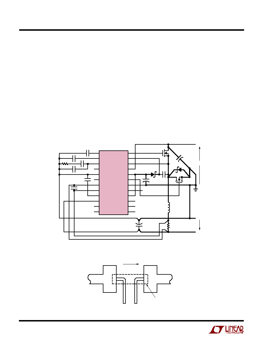
26
LTC1736
APPLICATIO S I FOR ATIO
W
U
U
U
Figure 10. LTC1736 Layout Diagram
1
2
3
4
5
6
7
8
9
10
11
12
24
23
22
21
20
19
18
17
16
15
14
13
C
OSC
RUN/SS
I
TH
FCB
SGND
PGOOD
SENSE
≠
SENSE
+
V
FB
V
OSENSE
VID0
VID1
TG
BOOST
SW
V
IN
INTV
CC
BG
PGND
EXTV
CC
VIDV
CC
VID4
VID3
VID2
LTC1736
1000pF
47pF
C
C1
C
OSC
C
C2
C
SS
R
C
+
4.7
µ
F
L1
EXTERNAL EXTV
CC
CONNECTION
D
B
C
IN
≠
≠
+
+
C
B
D1
M1
M2
+
R
SENSE
C
OUT
+
V
IN
V
OUT
1736 F10
SENSE
+
SENSE
≠
HIGH CURRENT PATH
1736 F11
CURRENT SENSE
RESISTOR
(R
SENSE
)
Figure 11. Kelvin Sensing R
SENSE
2. Does the V
OSENSE
pin connect as close as possible to
the load? The optional 50pF to 100pF capacitor from
V
FB
to SGND should be as close as possible to the
LTC1736.
3. Are the SENSE
≠
and SENSE
+
leads routed together with
minimum PC trace spacing? The filter capacitor be-
tween SENSE
+
and SENSE
≠
should be as close as
possible to the LTC1736. Ensure accurate current sens-
ing with kelvin connections as shown in Figure 11.
Series resistance can be added to the SENSE lines to
increase noise rejection.
4. Does the (+) terminal of C
IN
connect to the drain of the
topside MOSFET(s) as closely as possible? This capaci-
tor provides the AC current to the MOSFET(s).
5. Is the INTV
CC
decoupling capacitor connected closely
between
INTV
CC
and the power ground pin? This ca-
pacitor carries the MOSFET driver peak currents. An
additional 1
µ
F ceramic capacitor placed immediately
next to the INTV
CC
and PGND pins can help improve
noise performance.
6. Keep the switching node (SW), Top Gate node (TG) and
Boost node (BOOST) away from sensitive small-signal
nodes, especially from the voltage and current sensing
feedback pins. All of these nodes have very large and
fast moving signals and therefore should be kept on the
"output side" (Pins 13 to 24) of the LTC1736 and
occupy minimum PC trace area.
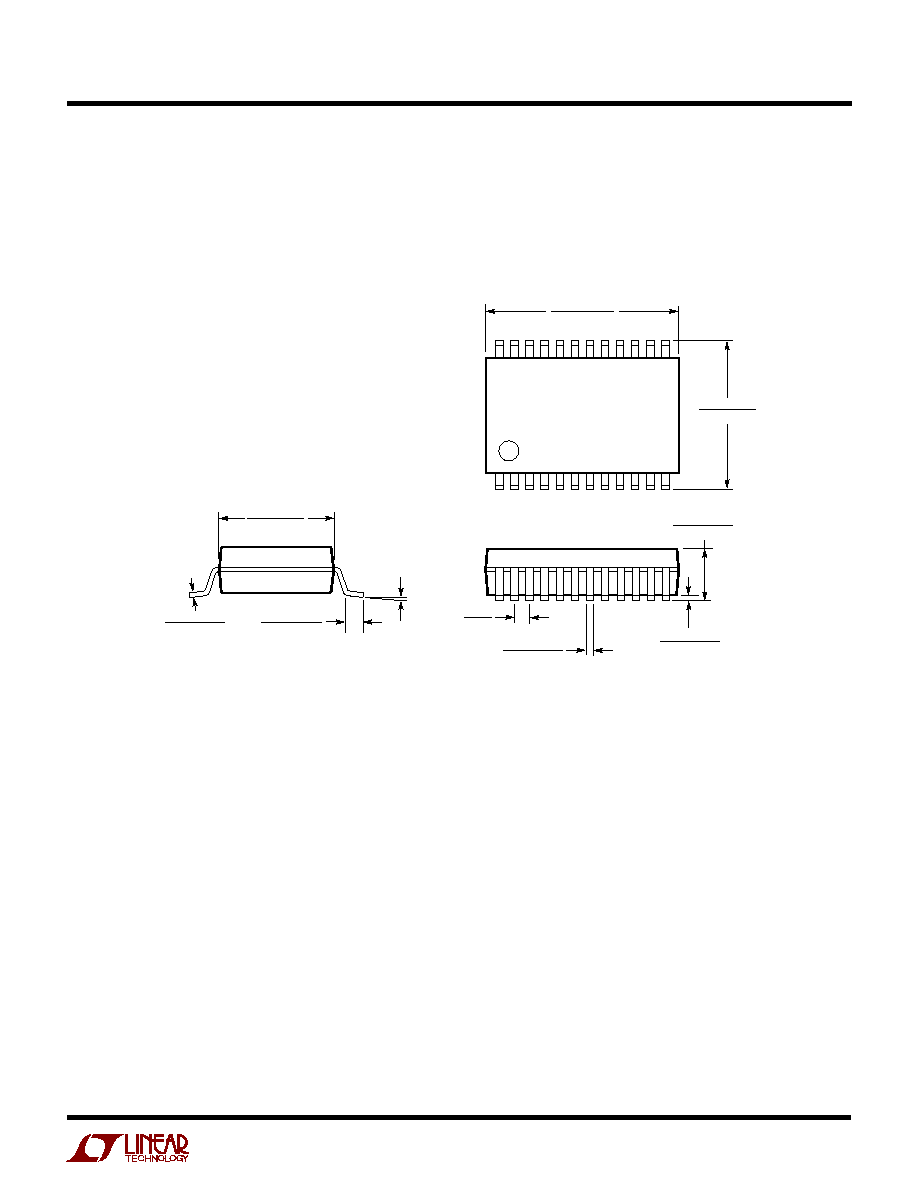
27
LTC1736
PACKAGE DESCRIPTIO
N
U
Dimensions in inches (millimeters) unless otherwise noted.
G Package
24-Lead Plastic SSOP (0.209)
(LTC DWG # 05-08-1640)
Information furnished by Linear Technology Corporation is believed to be accurate and reliable.
However, no responsibility is assumed for its use. Linear Technology Corporation makes no represen-
tation that the interconnection of its circuits as described herein will not infringe on existing patent rights.
G24 SSOP 1098
0.13 ≠ 0.22
(0.005 ≠ 0.009)
0
∞
≠ 8
∞
0.55 ≠ 0.95
(0.022 ≠ 0.037)
5.20 ≠ 5.38**
(0.205 ≠ 0.212)
7.65 ≠ 7.90
(0.301 ≠ 0.311)
1
2 3
4
5
6 7 8
9 10 11 12
8.07 ≠ 8.33*
(0.318 ≠ 0.328)
21
22
18 17 16 15 14 13
19
20
23
24
1.73 ≠ 1.99
(0.068 ≠ 0.078)
0.05 ≠ 0.21
(0.002 ≠ 0.008)
0.65
(0.0256)
BSC
0.25 ≠ 0.38
(0.010 ≠ 0.015)
NOTE: DIMENSIONS ARE IN MILLIMETERS
DIMENSIONS DO NOT INCLUDE MOLD FLASH. MOLD FLASH
SHALL NOT EXCEED 0.152mm (0.006") PER SIDE
DIMENSIONS DO NOT INCLUDE INTERLEAD FLASH. INTERLEAD
FLASH SHALL NOT EXCEED 0.254mm (0.010") PER SIDE
*
**
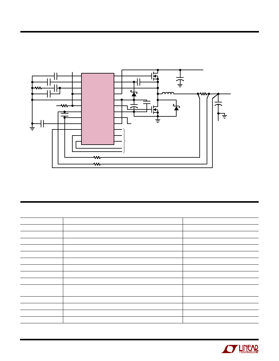
28
LTC1736
©
LINEAR TECHNOLOGY CORPORATION 1999
1736f LT/TP 1299 4K ∑ PRINTED IN USA
TYPICAL APPLICATIO
U
Linear Technology Corporation
1630 McCarthy Blvd., Milpitas, CA 95035-7417
(408) 432-1900
q
FAX: (408) 434-0507
q
www.linear-tech.com
12A Converter with FCB Tied to PGOOD for CPU Power; Optimized for Output Voltages of 1.3V to 1.6V
1
2
3
4
5
6
7
8
9
10
11
12
24
23
22
21
20
19
18
17
16
15
14
13
C
OSC
RUN/SS
I
TH
FCB
SGND
PGOOD
SENSE
≠
SENSE
+
V
FB
V
OSENSE
VID0
VID1
TG
BOOST
SW
V
IN
INTV
CC
BG
PGND
EXTV
CC
VIDV
CC
VID4
VID3
VID2
LTC1736
1000pF
47pF
C
C1
330pF
PGOOD
C
OSC
47pF
C
C2
47pF
C
SS
01.
µ
F
R
C
33k
100k
INTV
CC
+
4.7
µ
F
1
µ
F
D
B
CMDSH-3
D1
MBRS340T3
C
IN
22
µ
F/30V
◊
2
OS-CON
C
B
0.22
µ
F
M1
FDS6680A
L1
1.2
µ
H
R
SENSE
0.004
SGND
M2
FDS6680A
◊
2
OUTPUT VOLTAGE
PROGRAMMING
C
OUT
: 4-180
µ
F/4V PANASONIC EEFUEOG181R (AS SHOWN)
3-470
µ
F/6.3V KEMIT T51CX447M006AS (ALTERNATE)
1-820
µ
F/4V SANYO 4SP820M + 1-180
µ
F/4V PANASONIC EEFUE0G181R (ALTERNATE)
C
IN
: SANYO OS-CON 305C22M
L1: PANASONIC ETQP6RZ1RZ0HFA
10
OPTIONAL:
CONNECT
TO 5V
1736 TA02
+
C
OUT
180
µ
F/4V
◊
4
V
OUT
1.35V TO 1.6V
12A
V
IN
4.75V TO 24V
+
10
RELATED PARTS
PART NUMBER
DESCRIPTION
COMMENTS
LTC1147
High Efficiency Step-Down Controller
100% DC, Burst Mode Operation, SO-8
LTC1148HV/LTC1148
High Efficiency Synchronous Step-Down Controllers
100% DC, Burst Mode Operation, V
IN
< 20V
LTC1149
High Efficiency Synchronous Step-Down Controller
100% DC, Std Threshold MOSFETs, V
IN
< 48V
LTC1159
High Efficiency Synchronous Step-Down Controller
100% DC, Logic Level MOSFETs, V
IN
< 40V
LTC1265
1.2A Monolithic High Efficiency Step-Down Switching Regulator
100% DC, Burst Mode Operation, 14-Pin SO
LT1375/LT1376
1.5A 500kHz Step-Down Switching Regulators
High Efficiency, Constant Frequency, SO-8
LTC1435A
High Efficiency Synchronous Step-Down Controller, N-Ch Drive
Burst Mode Operation, 16-Pin Narrow SO
LTC1436A/LTC1436A-PLL High Efficiency Low Noise Synchronous Step-Down Converters, N-Ch Drive
Adaptive Power
TM
Mode, 20-Pin/24-Pin SSOP
LTC1474/LTC1475
Ultralow Quiescent Current Step-Down Monolithic Switching Regulators
I
Q
= 10
µ
A, 100% DC, 8-Pin MSOP
LTC1625/LTC1775
No R
SENSE
TM
Current Mode Synchronous Step-Down Controllers
Up to 97% Efficiency, Burst Mode Operation,
16-Pin SSOP
LTC1628
Dual High Efficiency 2-Phase Step-Down Controller
Antiphase Drive, 28-Pin SSOP Package
LTC1703
550kHz Dual Output Synchronous Step-Down DC/DC Controller
5-Bit, Mobile VID On Output 1, No R
SENSE
LTC1735
High Efficiency Synchronous Step-Down Controller, N-Ch Drive
Burst Mode Operation, 16-Pin Narrow SSOP
LTC1735-1
High Efficiency Step-Down Controller with Power Good
Output Fault Protection, 16-Pin SSOP and SO-8
Adaptive Power and No R
SENSE
are trademarks of Linear Technology Corporaton.