LTC2255/LTC2254
1
22554f
FEATURES
DESCRIPTIO
U
APPLICATIO S
U
TYPICAL APPLICATIO
U
Sample Rate: 125Msps/105Msps
Single 3V Supply (2.85V to 3.4V)
Low Power: 395mW/320mW
72.4dB SNR
88dB SFDR
No Missing Codes
Flexible Input: 1V
P-P
to 2V
P-P
Range
640MHz Full Power Bandwidth S/H
Clock Duty Cycle Stabilizer
Shutdown and Nap Modes
Pin Compatible Family
125Msps: LTC2253 (12-Bit), LTC2255 (14-Bit)
105Msps: LTC2252 (12-Bit), LTC2254 (14-Bit)
80Msps: LTC2229 (12-Bit), LTC2249 (14-Bit)
65Msps: LTC2228 (12-Bit), LTC2248 (14-Bit)
40Msps: LTC2227 (12-Bit), LTC2247 (14-Bit)
25Msps: LTC2226 (12-Bit), LTC2246 (14-Bit)
10Msps: LTC2225 (12-Bit), LTC2245 (14-Bit)
32-Pin (5mm
� 5mm) QFN Package
14-Bit, 125/105Msps
Low Power 3V ADCs
The LTC
�
2255/LTC2254 are 14-bit 125Msps/105Msps,
low power 3V A/D converters designed for digitizing high
frequency, wide dynamic range signals. The LTC2255/
LTC2254 are perfect for demanding imaging and commu-
nications applications with AC performance that includes
72.3dB SNR and 85dB SFDR for signals at the Nyquist
frequency.
DC specs include
�1LSB INL (typ), �0.5LSB DNL (typ) and
no missing codes over temperature. The transition noise
is a low 1.3 LSB
RMS
.
A single 3V supply allows low power operation. A separate
output supply allows the outputs to drive 0.5V to 3.3V
logic.
A single-ended CLK input controls converter operation. An
optional clock duty cycle stabilizer allows high perfor-
mance at full speed for a wide range of clock duty cycles.
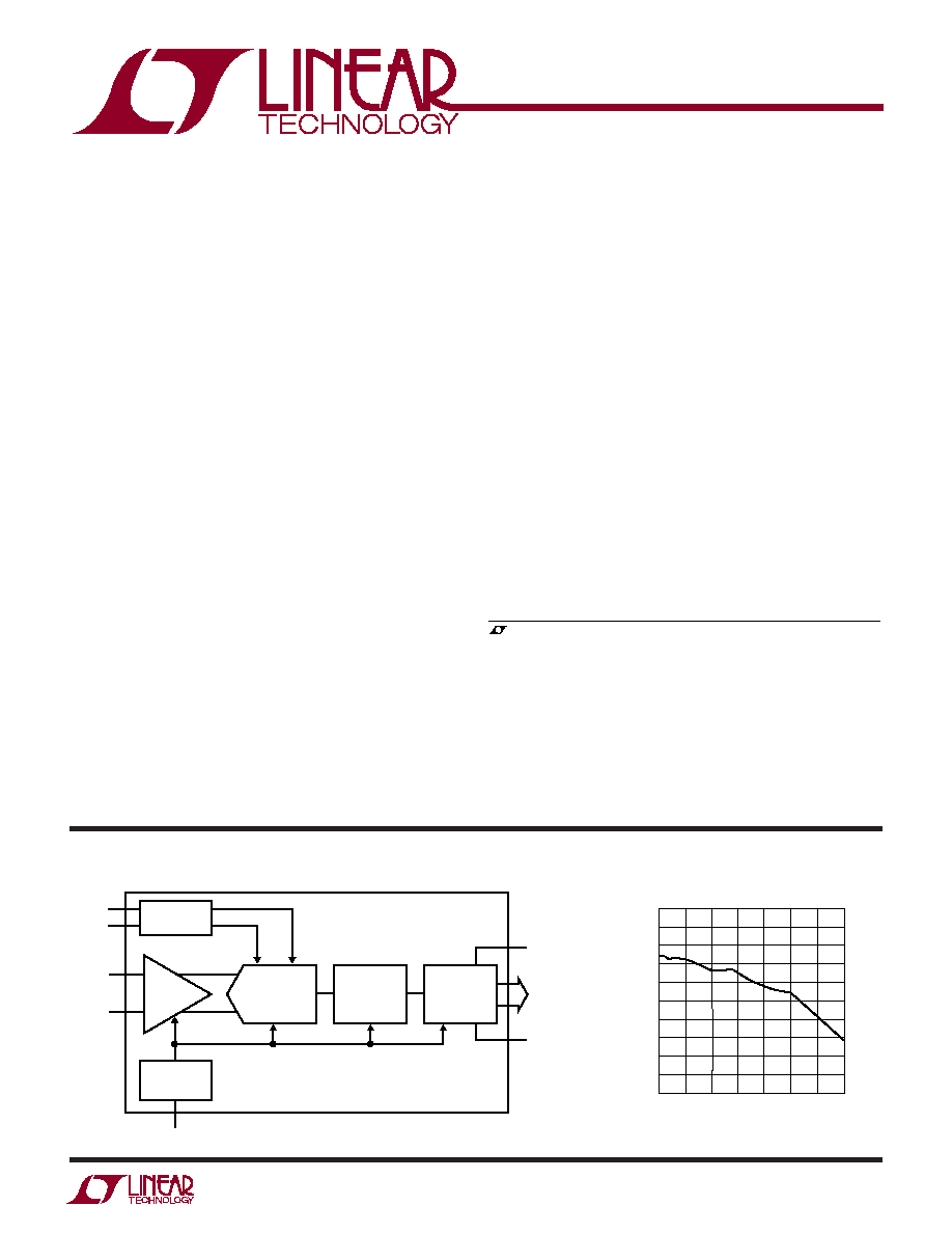
LTC2255: SNR vs Input Frequency,
�1dB, 2V Range, 125Msps
Wireless and Wired Broadband Communication
Imaging Systems
Ultrasound
Spectral Analysis
Portable Instrumentation
�
+
INPUT
S/H
CORRECTION
LOGIC
OUTPUT
DRIVERS
14-BIT
PIPELINED
ADC CORE
CLOCK/DUTY
CYCLE
CONTROL
FLEXIBLE
REFERENCE
D13
�
�
�
D0
CLK
REFH
REFL
ANALOG
INPUT
22554 TA01a
OV
DD
OGND
, LTC and LT are registered trademarks of Linear Technology Corporation.
All other trademarks are the property of their respective owners.
INPUT FREQUENCY (MHz)
0
65
SNR (dBFS)
66
68
69
70
75
72
100
200
250
33554 G09
67
73
74
71
50
150
300
350
LTC2255/LTC2254
2
22554f
ABSOLUTE AXI U
RATI GS
W
W
W
U
PACKAGE/ORDER I FOR ATIO
U
U
W
OV
DD
= V
DD
(Notes 1, 2)
Supply Voltage (V
DD
) ................................................. 4V
Digital Output Ground Voltage (OGND) ....... �0.3V to 1V
Analog Input Voltage (Note 3) ..... �0.3V to (V
DD
+ 0.3V)
Digital Input Voltage .................... �0.3V to (V
DD
+ 0.3V)
Digital Output Voltage ................ �0.3V to (OV
DD
+ 0.3V)
Power Dissipation ............................................ 1500mW
Operating Temperature Range
LTC2255C, LTC2254C ............................. 0
�C to 70�C
LTC2255I, LTC2254I ...........................�40
�C to 85�C
Storage Temperature Range ..................�65
�C to 125�C
Lead Temperature (Soldering, 10 sec).................. 300
�C
ORDER PART
NUMBER
QFN PART*
MARKING
T
JMAX
= 125
�C,
JA
= 34
�C/W
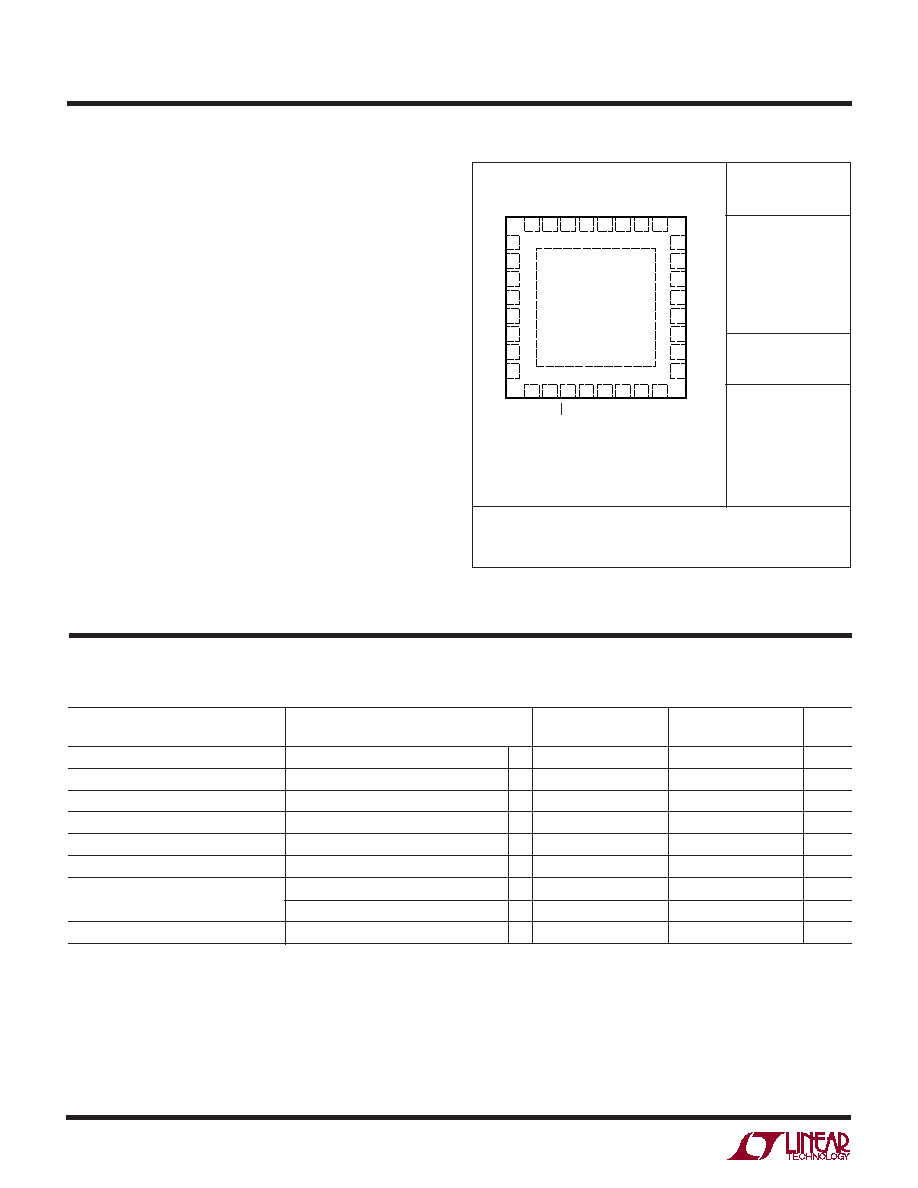
EXPOSED PAD (PIN 33) IS GND
MUST BE SOLDERED TO PCB
2255
2254
LTC2255CUH
LTC2255IUH
LTC2254CUH
LTC2254IUH
Consult LTC Marketing for parts specified with wider operating temperature ranges.
*The temperature grade is identified by a label on the shipping container.
32 31 30 29 28 27 26 25
9
10 11 12
TOP VIEW
UH PACKAGE
32-LEAD (5mm
� 5mm) PLASTIC QFN
13 14 15 16
17
18
19
20
21
22
23
24
8
7
6
5
4
3
2
1
AIN
+
AIN
�
REFH
REFH
REFL
REFL
V
DD
GND
D10
D9
D8
OV
DD
OGND
D7
D6
D5
V
DD
V
CM
SENSE
MODE
OF
D13
D12
D11
CLK
SHDN
OE
D0
D1
D2
D3
D4
33
The
denotes the specifications which apply over the full operating
temperature range, otherwise specifications are at T
A
= 25
�C. (Note 4)
LTC2255
LTC2254
PARAMETER
CONDITIONS
MIN
TYP
MAX
MIN
TYP
MAX
UNITS
Resolution (No Missing Codes)
14
14
Bits
Integral Linearity Error
Differential Analog Input (Note 5)
�5
�1
5
�5.5
�1
5.5
LSB
Differential Linearity Error
Differential Analog Input
�1
�0.5
1
�1
�0.5
1
LSB
Offset Error
(Note 6)
�12
�2
12
�12
�2
12
mV
Gain Error
External Reference
�2.5
�0.5
2.5
�2.5
�0.5
2.5
%FS
Offset Drift
�10
�10
�V/�C
Full-Scale Drift
Internal Reference
�30
�30
ppm/
�C
External Reference
�5
�5
ppm/
�C
Transition Noise
SENSE = 1V
1.3
1.3
LSB
RMS
CO VERTER CHARACTERISTICS
U
Order Options Tape and Reel: Add #TR
Lead Free: Add #PBF Lead Free Tape and Reel: Add #TRPBF
Lead Free Part Marking:
http://www.linear.com/leadfree/
LTC2255/LTC2254
3
22554f
LTC2255
LTC2254
SYMBOL
PARAMETER
CONDITIONS
MIN
TYP
MAX
MIN
TYP
MAX
UNITS
SNR
Signal-to-Noise Ratio
5MHz Input
72.4
72.5
dB
30MHz Input
72.3
72.4
dB
70MHz Input
68.9
72.1
69.4
72.3
dB
140MHz Input
71.7
71.7
dB
SFDR
5MHz Input
88
88
dB
30MHz Input
85
88
dB
70MHz Input
73
82
71
84
dB
140MHz Input
78
80
dB
SFDR
5MHz Input
90
90
dB
30MHz Input
90
90
dB
70MHz Input
77
90
79
90
dB
140MHz Input
90
90
dB
S/(N+D)
5MHz Input
72.2
72.4
dB
30MHz Input
72
72.2
dB
70MHz Input
68
71.9
68.5
72
dB
140MHz Input
70.2
70.6
dB
IMD
Intermodulation
f
IN1
= 28.2MHz
85
85
dB
Distortion
f
IN2
= 26.8MHz
SYMBOL
PARAMETER
CONDITIONS
MIN
TYP
MAX
UNITS
V
IN
Analog Input Range (A
IN
+
�A
IN
�
)
2.85V < V
DD
< 3.4V (Note 7)
�0.5V to �1V
V
V
IN,CM
Analog Input Common Mode
Differential Input (Note 7)
1
1.5
1.9
V
I
IN
Analog Input Leakage Current
0V < A
IN
+
, A
IN
�
< V
DD
�1
1
�A
I
SENSE
SENSE Input Leakage
0V < SENSE < 1V
�3
3
�A
I
MODE
MODE Pin Leakage
�3
3
�A
t
AP
Sample-and-Hold Acquisition Delay Time
0
ns
t
JITTER
Sample-and-Hold Acquisition Delay Time Jitter
0.2
ps
RMS
CMRR
Analog Input Common Mode Rejection Ratio
80
dB
Full Power Bandwidth
Figure 8 Test Circuit
640
MHz
The
denotes the specifications which apply over the full operating temperature range,
otherwise specifications are at T
A
= 25
�C. A
IN
= �1dBFS. (Note 4)
A ALOG I PUT
U
U
DY
A
IC ACCURACY
U
W
The
denotes the specifications which apply over the full operating temperature range, otherwise
specifications are at T
A
= 25
�C. (Note 4)
Signal-to-Noise Plus
Distortion Ratio
Spurious Free Dynamic Range
4th Harmonic or Higher
Spurious Free Dynamic Range
2nd or 3rd Harmonic
LTC2255/LTC2254
4
22554f
DIGITAL I PUTS A D DIGITAL OUTPUTS
U
U
The
denotes the specifications which apply over the
full operating temperature range, otherwise specifications are at T
A
= 25
�C. (Note 4)
I TER AL REFERE CE CHARACTERISTICS
U
U
U
(Note 4)
POWER REQUIRE E TS
W
U
The
denotes the specifications which apply over the full operating temperature
range, otherwise specifications are at T
A
= 25
�C. (Note 8)
LTC2255
LTC2254
SYMBOL
PARAMETER
CONDITIONS
MIN
TYP
MAX
MIN
TYP
MAX
UNITS
V
DD
Analog Supply Voltage
(Note 9)
2.85
3
3.4
2.85
3
3.4
V
OV
DD
Output Supply Voltage
(Note 9)
0.5
3
3.6
0.5
3
3.6
V
IV
DD
Supply Current
132
156
107
126
mA
P
DISS
Power Dissipation
395
468
320
378
mW
P
SHDN
Shutdown Power
SHDN = H,
2
2
mW
OE = H, No CLK
P
NAP
Nap Mode Power
SHDN = H,
15
15
mW
OE = L, No CLK
PARAMETER
CONDITIONS
MIN
TYP
MAX
UNITS
V
CM
Output Voltage
I
OUT
= 0
1.475
1.500
1.525
V
V
CM
Output Tempco
�25
ppm/
�C
V
CM
Line Regulation
2.85V < V
DD
< 3.4V
3
mV/V
V
CM
Output Resistance
�1mA < I
OUT
< 1mA
4
SYMBOL
PARAMETER
CONDITIONS
MIN
TYP
MAX
UNITS
LOGIC INPUTS (CLK, OE, SHDN)
V
IH
High Level Input Voltage
V
DD
= 3V
2
V
V
IL
Low Level Input Voltage
V
DD
= 3V
0.8
V
I
IN
Input Current
V
IN
= 0V to V
DD
�10
10
�A
C
IN
Input Capacitance
(Note 7)
3
pF
LOGIC OUTPUTS
OV
DD
= 3V
C
OZ
Hi-Z Output Capacitance
OE = High (Note 7)
3
pF
I
SOURCE
Output Source Current
V
OUT
= 0V
50
mA
I
SINK
Output Sink Current
V
OUT
= 3V
50
mA
V
OH
High Level Output Voltage
I
O
= �10
�A
2.995
V
I
O
= �200
�A
2.7
2.99
V
V
OL
Low Level Output Voltage
I
O
= 10
�A
0.005
V
I
O
= 1.6mA
0.09
0.4
V
OV
DD
= 2.5V
V
OH
High Level Output Voltage
I
O
= �200
�A
2.49
V
V
OL
Low Level Output Voltage
I
O
= 1.6mA
0.09
V
OV
DD
= 1.8V
V
OH
High Level Output Voltage
I
O
= �200
�A
1.79
V
V
OL
Low Level Output Voltage
I
O
= 1.6mA
0.09
V
LTC2255/LTC2254
5
22554f
TI I G CHARACTERISTICS
U
W
The
denotes the specifications which apply over the full operating temperature
range, otherwise specifications are at T
A
= 25
�C. (Note 4)
Note 1: Absolute Maximum Ratings are those values beyond which the life
of a device may be impaired.
Note 2: All voltage values are with respect to ground with GND and OGND
wired together (unless otherwise noted).
Note 3: When these pin voltages are taken below GND or above V
DD
, they
will be clamped by internal diodes. This product can handle input currents
of greater than 100mA below GND or above V
DD
without latchup.
Note 4: V
DD
= 3V, f
SAMPLE
= 125MHz (LTC2255) or 105MHz (LTC2254),
input range = 2V
P-P
with differential drive, clock duty cycle stabilizer on,
unless otherwise noted.
Note 5: Integral nonlinearity is defined as the deviation of a code from a
straight line passing through the actual endpoints of the transfer curve.
The deviation is measured from the center of the quantization band.
Note 6: Offset error is the offset voltage measured from �0.5 LSB when
the output code flickers between 00 0000 0000 0000 and
11 1111 1111 1111.
Note 7: Guaranteed by design, not subject to test.
Note 8: V
DD
= 3V, f
SAMPLE
= 125MHz (LTC2255) or 105MHz (LTC2254),
input range = 1V
P-P
with differential drive.
Note 9: Recommended operating conditions.
LTC2255
LTC2254
SYMBOL
PARAMETER
CONDITIONS
MIN
TYP
MAX
MIN
TYP
MAX
UNITS
f
s
Sampling Frequency
(Note 9)
1
125
1
105
MHz
t
L
CLK Low Time
Duty Cycle Stabilizer Off
3.8
4
500
4.5
4.76
500
ns
Duty Cycle Stabilizer On
3
4
500
3
4.76
500
ns
(Note 7)
t
H
CLK High Time
Duty Cycle Stabilizer Off
3.8
4
500
4.5
4.76
500
ns
Duty Cycle Stabilizer On
3
4
500
3
4.76
500
ns
(Note 7)
t
AP
Sample-and-Hold
0
0
ns
Aperture Delay
t
D
CLK to DATA delay
C
L
= 5pF (Note 7)
1.4
2.7
5.4
1.4
2.7
5.4
ns
Data Access Time
C
L
= 5pF (Note 7)
4.3
10
4.3
10
ns
After OE
BUS Relinquish Time
(Note 7)
3.3
8.5
3.3
8.5
ns
Pipeline Latency
6
6
Cycles