 | ÐлекÑÑоннÑй компоненÑ: LTC1753CG | СкаÑаÑÑ:  PDF PDF  ZIP ZIP |
Äîêóìåíòàöèÿ è îïèñàíèÿ www.docs.chipfind.ru
1
LTC1753
5-Bit Programmable
Synchronous Switching
Regulator Controller for
Pentium
®
III Processor
The LTC
®
1753 is a high power, high efficiency switching
regulator controller optimized for 5V input to a digitally
programmable 1.3V-3.5V output. The internal 5-bit DAC
programs the output voltage from 1.3V to 2.05V in 50mV
increments and from 2.1V to 3.5V in 100mV increments. The
precision internal reference and an internal feedback system
provide an output accuracy of
±
1.5% at room temperature
and typically
±
2% over temperature, load current and line
voltage shifts. The LTC1753 uses a synchronous switching
architecture with two external N-channel output devices,
providing high efficiency and eliminating the need for a high
power, high cost P-channel device. Additionally, it senses the
output current across the on-resistance of the upper N-
channel FET, providing an adjustable current limit without an
external low value sense resistor.
The LTC1753 free-runs at 300kHz and can be synchronized
to a faster external clock if desired. It provides a phase lead
compensation scheme and under harsh loading conditions,
the PWM duty cycle can be momentarily forced to 0% or
100% to reduce the output voltage recovery time.
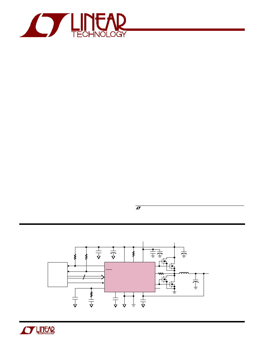
Figure 1. 5V to 1.3V-3.5V Supply Application
, LTC and LT are registered trademarks of Linear Technology Corporation.
Pentium is a registered trademark of Intel Corporation.
AMD-K6 is a registered trademark of Advanced Micro Devices, Inc.
s
5-Bit Digitally Programmable 1.3V to 3.5V Fixed
Output Voltage, VRM 8.4 Compliant
s
Fast Transient Response: 0% to 100% Duty Cycle
s
Phase Lead Compensation for Remote Sensing
s
Overtemperature Protection
s
Flags for Power Good and Overvoltage Fault
s
19A Output Current Capability from a 5V Supply
s
Dual N-Channel MOSFET Synchronous Driver
s
Initial Output Accuracy:
±
1.5%
s
Excellent Output Accuracy:
±
2% Typ Over Line,
Load and Temperature Variations
s
High Efficiency: Over 95% Possible
s
Adjustable Current Limit Without External Sense
Resistors
s
Available in 2O-Lead SSOP and SW Packages
s
Power Supply for Pentium
®
III, AMD-K6
®
-2, SPARC,
ALPHA and PA-RISC Microprocessors
s
High Power 5V to 1.3V-3.5V Regulators
PWRGD
FAULT
VID0 TO VID4
OUTEN
COMP
SS
SGND
GND
SENSE
10
µ
F
Q1*
20
Q2*
Q2A*
Q1A*
0.1
µ
F
V
CC
I
MAX
PV
CC
PV
CC
12V
V
IN
5V
L
O
1.3
µ
H
18A
LTC1753
G1
I
FB
V
FB
+
1
µ
F
NC
1753 F01
C
C
4700pF
R
C
15k
600
5.6k
5.6k
C
SS
0.1
µ
F
+
0.1
µ
F
10
µ
F
C
IN
**
1200
µ
F
×
4
V
OUT
1.3V TO
3.5V
14A
C
OUT
2700
µ
F
×
5
+
C1
150pF
+
5
* SILICONIX SUD50N03-10
** SANYO 10MV1200GX
PANASONIC ETQP 6FIR3LFA
SANYO 6MV2700GX
CPU
G2
DESCRIPTIO
U
FEATURES
APPLICATIO S
U
TYPICAL APPLICATIO
U
2
LTC1753
ORDER PART
NUMBER
Consult factory for Industrial and Military grade parts.
T
JMAX
= 125
°
C,
JA
= 100
°
C/ W (G)
T
JMAX
= 125
°
C,
JA
= 100
°
C/ W (SW)
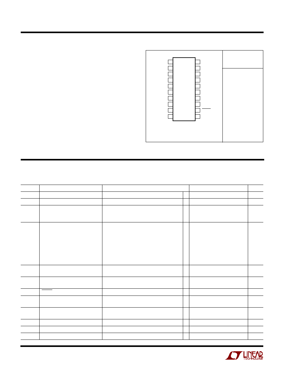
1
2
3
4
5
6
7
8
9
10
TOP VIEW
G PACKAGE
20-LEAD PLASTIC SSOP
SW PACKAGE
20-LEAD PLASTIC SO
20
19
18
17
16
15
14
13
12
11
G2
PV
CC
GND
SGND
V
CC
SENSE
I
MAX
I
FB
SS
COMP
G1
OUTEN
VID0
VID1
VID2
VID3
VID4
PWRGD
FAULT
V
FB
LTC1753CG
LTC1753CSW
(Note 1)
Supply Voltage
V
CC
........................................................................ 7V
PV
CC
................................................................... 14V
Input Voltage
I
FB
(Note 2) ............................................ PV
CC
+ 0.3V
I
MAX
........................................................ 0.3V to 9V
All Other Inputs ...................... 0.3V to (V
CC
+ 0.3V)
Digital Output Voltage ................................. 0.3V to 9V
I
FB
Input Current (Notes 2, 3) .......................... 100mA
Junction Temperature .......................................... 125
°
C
Operating Temperature Range ..................... 0
°
C to 70
°
C
Storage Temperature Range ................. 65
°
C to 150
°
C
Lead Temperature (Soldering, 10 sec.)................. 300
°
C
SYMBOL
PARAMETER
CONDITIONS
MIN
TYP
MAX
UNITS
V
CC
Supply Voltage
q
4.5
6
V
PV
CC
Supply Voltage for G1, G2
q
13.2
V
V
FB
Internal Feedback Voltage
1.3V Output Voltage
0.5
V
2.1V Initial Output Voltage
0.8
V
3.5V Initial Output Voltage
1.34
V
V
OUT
1.3V Initial Output Voltage
With Respect to Rated Output Voltage (Figure 2)
20 ( 1.5%)
20 (+ 1.5%)
mV
1.8V Initial Output Voltage
27 ( 1.5%)
27 (+ 1.5%)
mV
2.8V Initial Output Voltage
42 ( 1.5%)
42 (+ 1.5%)
mV
3.5V Initial Output Voltage
52 ( 1.5%)
52 (+ 1.5%)
mV
1.3V Initial Output Voltage
q
26 ( 2%)
26 (+ 2%)
mV
1.8V Initial Output Voltage
q
36 ( 2%)
36 (+ 2%)
mV
2.8V Initial Output Voltage
q
56 ( 2%)
56 (+ 2%)
mV
3.5V Initial Output Voltage
q
70 ( 2%)
70 (+ 2%)
mV
V
OUT
Output Load Regulation
I
OUT
= 0 to 14A (Figure 2)
5
mV
Output Line Regulation
V
IN
= 4.75V to 5.25V, I
OUT
= 0 (Figure 2)
±
1
mV
V
PWRGD
Positive Power Good Trip Point
% Above Output Voltage (Note 4) (Figure 2)
q
3
6
%
Negative Power Good Trip Point
% Below Output Voltage (Note 4) (Figure 2)
q
6
3
%
V
FAULT
FAULT Trip Point
% Above Output Voltage (Note 4) (Figure 2)
q
8
13
18
%
I
CC
Operating Supply Current
OUTEN = V
CC
= 5V (Note 5)(Figure 3)
q
800
1200
µ
A
Shutdown Supply Current
OUTEN = 0, VID0 to VID4 Floating (Figure 3)
q
130
250
µ
A
I
PVCC
Supply Current
PV
CC
= 12V, OUTEN = V
CC
(Note 6) (Figure 3)
15
mA
PV
CC
= 12V, OUTEN = 0, VID0 to VID4 Floating
1
µ
A
f
OSC
Internal Oscillator Frequency
(Figure 4)
q
250
300
350
kHz
V
SAWL
V
COMP
at Minimum Duty Cycle
(Note 11)
1.8
V
V
SAWH
V
COMP
at Maximum Duty Cycle
(Note 11)
2.8
V
ABSOLUTE AXI U RATI GS
W
W
W
U
PACKAGE/ORDER I FOR ATIO
U
U
W
ELECTRICAL CHARACTERISTICS
The
q
denotes specifications which apply over the full operating temperature range, otherwise specifications are at T
A
= 25
°
C.
V
CC
= 5V, PV
CC
= 12V, unless otherwise noted. (Note 3)
3
LTC1753
Note 1: Absolute Maximum Ratings are those values beyond which the life
of a device may be impaired.
Note 2: When I
FB
is taken below GND, it will be clamped by an internal diode.
This pin can handle input currents greater than 100mA below GND without
latchup. In the positive direction, it is not clamped to V
CC
or PV
CC
.
Note 3: All currents into device pins are positive; all currents out of the
device pins are negative. All voltages are referenced to ground unless
otherwise specified.
Note 4: The Power Good and FAULT trip thresholds are tested at the 1.8V
output voltage code. The Power Good and FAULT trip thresholds are
guaranteed by design for all other output voltage codes to the same
specification.
Note 5: The LTC1753 goes into the shutdown mode if VID0 to VID4 are
floating. Due to the internal pull-up resistors, there will be an additional
0.25mA/pin if any of the VID0 to VID4 pins are pulled low.
Note 6: Supply current in normal operation is dominated by the current
needed to charge and discharge the external FET gates. This will vary with
SYMBOL
PARAMETER
CONDITIONS
MIN
TYP
MAX
UNITS
G
ERR
Error Amplifier Open-Loop DC Gain
(Note 7)
q
40
54
dB
g
mERR
Error Amplifier Transconductance
(Note 7)
q
0.9
1.6
2.3
millimho
BW
ERR
Error Amplifier 3dB Bandwidth
COMP = Open (Note 11)
400
kHz
I
IMAX
I
MAX
Sink Current
V
IMAX
= V
CC
q
150
190
230
µ
A
I
SS
Soft-Start Source Current
V
SS
= 0V, V
IMAX
= 0V, V
IFB
= V
CC
q
16
12
8
µ
A
I
SSIL
Maximum Soft-Start Sink Current
V
SENSE
= V
OUT
, V
IMAX
= V
CC
, V
IFB
= 0V
q
30
60
150
µ
A
Under Current Limit
(Notes 8, 9), V
SS
= V
CC
I
SSHIL
Soft-Start Sink Current Under Hard
V
SENSE
= 0V, V
IMAX
= V
CC
, V
IFB
= 0V
q
20
45
mA
Current Limit
t
SSHIL
Hard Current Limit Hold Time
V
SENSE
= 0V, V
IMAX
= 4V, V
IFB
from 5V
500
µ
s
t
PWRGD
Power Good Response Time
V
SENSE
from 0V to Rated V
OUT
q
0.5
1
2
ms
t
PWRBAD
Power Good Response Time
V
SENSE
from Rated V
OUT
to 0V
q
200
500
1000
µ
s
t
FAULT
FAULT Response Time
V
SENSE
from Rated V
OUT
to V
CC
q
200
500
1000
µ
s
V
OTDD
Overtemperature Driver Disable
OUTEN
, VID0 to VID4 = 0 (Note 10) (Figure 3)
q
1.6
1.7
1.8
V
V
SHDN
Shutdown
OUTEN
, VID0 to VID4 = 0 (Note 10) (Figure 3)
q
0.8
V
t
r
, t
f
Driver Rise and Fall Time
(Figure 4)
q
90
150
ns
t
NOL
Driver Nonoverlap Time
(Figure 4)
q
30
100
ns
V
IH
VID0 to VID4 Input High Voltage
q
2
V
V
IL
VID0 to VID4 Input Low Voltage
q
0.8
V
R
SENSE
SENSE Input Resistance
108
k
R
VID
VID0 to VID4 Internal Pull-Up
q
10
20
k
Resistance
I
SINK
Digital Output Sink Current
q
10
mA
the LTC1753 operating frequency, supply voltage and the external FETs
used.
Note 7: The open-loop DC gain and transconductance from the SENSE pin to
COMP pin will be (G
ERR
)(1.26/3.3) and (g
mERR
)(1.26/3.3) respectively.
Note 8: The current limiting amplifier can sink but cannot source current.
Under normal (not current limited) operation, the output current will be zero.
Note 9: Under typical soft current limit, the net soft-start discharge current
will be 60
µ
A (I
SSIL
) + [ 12
µ
A(I
SS
)]
48
µ
A. The soft-start sink-to-source
current ratio is designed to be 5:1.
Note 10: When VID0 to VID4 are all HIGH, the LTC1753 will be forced to
shut down internally. The OUTEN trip voltages are guaranteed by design for
all other input codes.
Note 11: This parameter is guaranteed by design and correlation and is not
tested in production.
ELECTRICAL CHARACTERISTICS
The
q
denotes specifications which apply over the full operating temperature range, otherwise specifications are at T
A
= 25
°
C.
V
CC
= 5V, PV
CC
= 12V, unless otherwise noted. (Note 3)
4
LTC1753
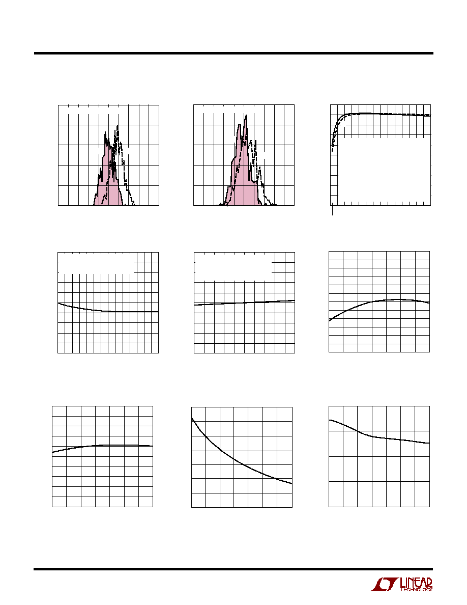
Efficiency vs Load Current
LOAD CURRENT (A)
0
EFFICIENCY (%)
60
80
100
4
1753 G03
40
20
50
70
90
A
30
10
0
0.3
2
6
8
10
12
14
B
REFER TO TYPICAL APPLICATION
CIRCUIT FIGURE 1
V
IN
= 5V, PV
CC
= 12V, V
OUT
= 2.8V,
C
OUT
= 330
µ
F
×
7, L
O
= 2
µ
H
A: Q1 = 1
×
SUD50N03-10
Q2 = 1
×
SUD50N03-10
B: Q1 = 2
×
SUD50N03-10
Q2 = 1
×
SUD50N03-10
NO FAN
Q1 IS MOUNTED ON 1IN
2
COPPER AREA
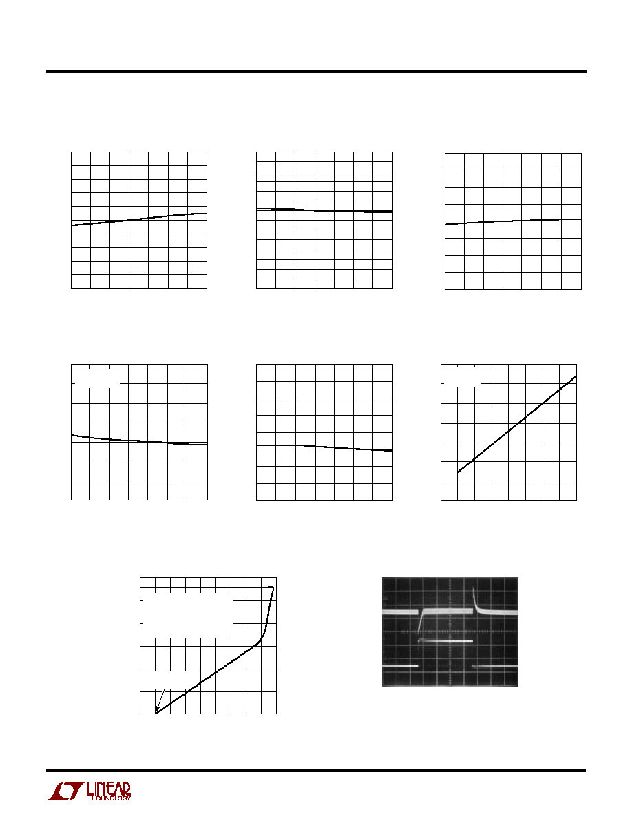
Error Amplifier Open-Loop
DC Gain vs Temperature
Overtemperature Driver Disable
vs Temperature
Load Regulation
Line Regulation
OUTPUT CURRENT (A)
0
OUTPUT VOLTAGE (V)
2.825
4
1753 G04
2.820
2.815
2.810
2.805
2.800
2.795
2.790
2.785
2.780
2.775
1 2 3
5 6 7 8 9 10 11 12 13 14
REFER TO TYPICAL APPLICATION
CIRCUIT FIGURE 1
V
IN
= 5V, PV
CC
= 12V, T
A
= 25
°
C
INPUT VOLTAGE (V)
4.75
OUTPUT VOLTAGE (V)
2.825
2.820
2.815
2.810
2.805
2.800
2.795
2.790
2.785
2.780
2.775
5.15
1753 G05
4.85
4.95
5.05
5.25
REFER TO TYPICAL APPLICATION
CIRCUIT FIGURE 1
OUTPUT = NO LOAD
T
A
= 25
°
C
Output Temperature Drift
TEMPERATURE (
°
C)
50
OUTPUT VOLTAGE (V)
2.860
2.850
2.840
2.830
2.820
2.810
2.800
2.790
2.780
2.770
2.750
2.760
2.740
0
50
75
1753 G06
25
25
100
125
TEMPERATURE (
°
C)
50
1.60
OVER-TEMPERATURE DRIVER DISABLE (V)
1.62
1.66
1.68
1.70
1.80
1.74
0
50
75
1753 G07
1.64
1.76
1.78
1.72
25
25
100
125
TEMPERATURE (
°
C)
50
40
ERROR AMPLIFIER OPEN-LOOP DC GAIN (dB)
45
50
55
60
25
0
25
50
1753 G09
75
100
125
Typical 1.3V V
OUT
Distribution
OUTPUT VOLTAGE (V)
1.275
NUMBER OF UNITS
30
40
50
1.315
1753 G01
20
10
0
1.285
1.295
1.305
1.325
100
°
C
TOTAL SAMPLE SIZE = 500
25
°
C
Error Amplifier Transconductance
vs Temperature
TEMPERATURE (
°
C)
50
1.7
1.9
2.3
25
75
1753 G08
1.5
1.3
25
0
50
100
125
1.1
0.9
2.1
ERROR AMPLIFIER TRANSCONDUCTANCE (millimho)
OUTPUT VOLTAGE (V)
2.75
NUMBER OF UNITS
30
40
50
2.83
1753 G02
20
10
0
2.77
2.79
2.81
2.85
100
°
C
TOTAL SAMPLE SIZE = 500
25
°
C
Typical 2.8V V
OUT
Distribution
TYPICAL PERFOR A CE CHARACTERISTICS
U
W
5
LTC1753
Soft-Start Source Current
vs Temperature
Oscillator Frequency
vs Temperature
I
MAX
Sink Current
vs Temperature
TEMPERATURE (
°
C)
50
250
OSCILLATOR FREQUENCY (kHz)
260
280
290
300
350
320
0
50
75
1753 G10
270
330
340
310
25
25
100
125
TEMPERATURE (
°
C)
50
150
I
MAX
SINK CURRENT (
µ
A)
160
170
180
220
200
25
25
50
125
1753 G11
210
190
0
75
100
TEMPERATURE (
°
C)
50
SOFT START SOURCE CURRENT (
µ
A)
9
8
25
75
1753 G12
10
11
25
0
50
100
125
12
13
14
16
15
V
CC
Operating Supply Current
vs Temperature
PV
CC
Supply Current
vs Gate Capacitance
V
CC
Shutdown Supply Current
vs Temperature
50
µ
s/DIV
1753 G17
Transient Response, V
OUT
= 2.8V
Output Over Current Protection
TEMPERATURE (
°
C)
50
0.9
1.0
1.2
25
75
1753 G13
0.8
0.7
25
0
50
100
125
0.6
0.5
1.1
V
CC
OPERATING SUPPLY CURRENT (mA)
V
CC
= 5V
f
OSC
= 300kHz
TEMPERATURE (
°
C)
50
V
CC
SHUTDOWN SUPPLY CURRENT (
µ
A)
225
25
1753 G14
150
100
25
0
50
75
50
250
200
175
125
75
100
125
GATE CAPACITANCE (pF)
0
PV
CC
SUPPLY CURRENT (mA)
40
50
60
6000
1753 G15
30
20
2000
4000
8000
10
0
70
PV
CC
= 12V
T
A
= 25
°
C
OUTPUT CURRENT (A)
0
0
OUTPUT VOLTAGE (V)
0.5
1.5
2.0
2.5
4
8
10
18
1753 G16
1.0
2
6
12
14
16
3.0
Q1 CASE = 90
°
C, V
OUT
= 2.8V
Q1 = 2
×
MTD20N03HDL
Q2 = 1
×
MTD20N03HDL
R
IMAX
= 2.7k, R
IFB
= 20
,
SS CAP = 0.01
µ
F
SHORT-CIRCUIT
CURRENT
V
OUT
50mV/DIV
0
I
LOAD
5A/DIV
10
TYPICAL PERFOR A CE CHARACTERISTICS
U
W