1772f Layout
1
LTC1772
1772fs, sn1772
Constant Frequency
Current Mode Step-Down
DC/DC Controller in SOT-23
The LTC
®
1772 is a constant frequency current mode step-
down DC/DC controller providing excellent AC and DC load
and line regulation. The device incorporates an accurate
undervoltage lockout feature that shuts down the LTC1772
when the input voltage falls below 2.0V.
The LTC1772 provides a
±
2.5% output voltage accuracy
and consumes only 270
µ
A of quiescent current. For
applications where efficiency is a prime consideration, the
LTC1772 is configured for Burst Mode operation, which
enhances efficiency at low output current.
To further maximize the life of a battery source, the
external P-channel MOSFET is turned on continuously in
dropout (100%dutycycle).In shutdown, the device draws
a mere 8
µ
A. High constant operating frequency of 550kHz
allows the use of a small external inductor.
The LTC1772 is available in a small footprint 6-lead
SOT-23.
s
One or Two Lithium-Ion-Powered Applications
s
Cellular Telephones
s
Wireless Modems
s
Portable Computers
s
Distributed 3.3V, 2.5V or 1.8V Power Systems
s
Scanners
s
High Efficiency: Up to 94%
s
High Output Currents Easily Achieved
s
Wide V
IN
Range: 2.5V to 9.8V
s
Constant Frequency 550kHz Operation
s
Burst Mode
®
Operation at Light Load
s
Low Dropout: 100% Duty Cycle
s
Tiny 6-Lead SOT-23 Package
s
0.8V Reference Allows Low Output Voltages
s
Current Mode Operation for Excellent Line and Load
s
Transient Response
s
Low Quiescent Current: 270
µ
A
s
Shutdown Mode Draws Only 8
µ
A Supply Current
s
±
2.5% Reference Accuracy
, LTC and LT are registered trademarks of Linear Technology Corporation.
Burst Mode is a registered trademark of Linear Technology Corporation.
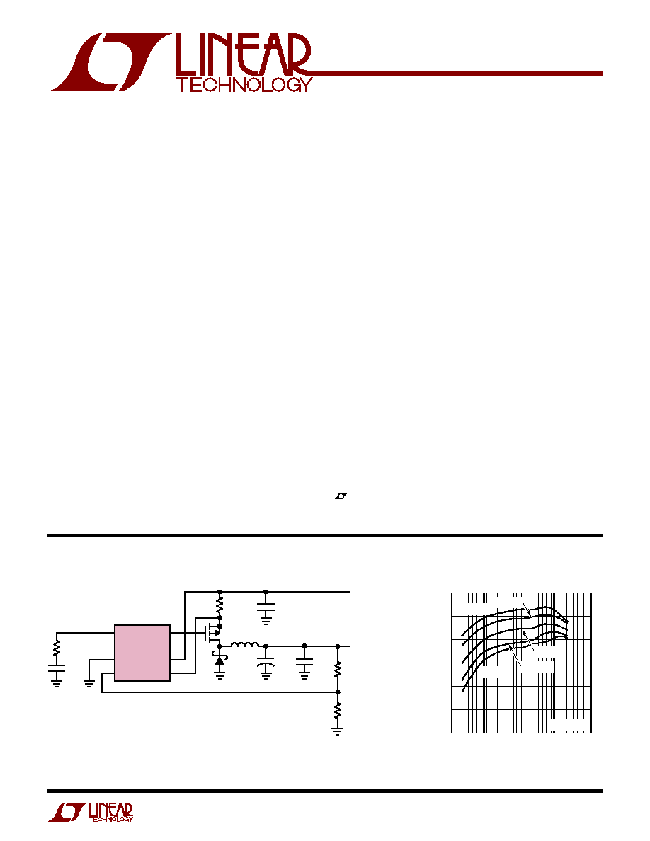
Figure 1. High Efficiency, High Output Current 2.5V/2A Regulator
APPLICATIO S
U
FEATURES
TYPICAL APPLICATIO
U
DESCRIPTIO
U
I
TH
/RUN
LTC1772
10k
R1
0.03
174k
80.6k
L1
4.7
µ
H
M1
D1
220pF
C1: TAIYO YUDEN LMK325BJ106K-T
C2A: SANYO 6TPA47M
C2B: AVX 0805ZC105KAT1A
D1: MOTOROLA MBRM120T3
L1: MURATA LQN6C-4R7
M1: FAIRCHILD FDC638P
R1: IRC LRC-LR1206-01-R030F
GND
V
FB
6
5
4
1772 F01a
1
2
3
PGATE
V
IN
SENSE
C1
10
µ
F
10V
C2B
1
µ
F
10V
V
IN
2.5V
TO 9.8V
V
OUT
2.5V
2A
C2A
47
µ
F
6V
+
LOAD CURRENT (mA)
EFFICIENCY (%)
100
90
80
70
60
50
40
100
1000
10000
10
1
V
OUT
= 2.5V
V
IN
= 6V
1772 F01b
V
IN
= 8.4V
V
IN
= 9.8V
V
IN
= 3.3V
V
IN
= 4.2V
Efficiency vs Load Current
2
LTC1772
1772fs, sn1772
Note 1: Absolute Maximum Ratings are those values beyond which the life
of a device may be impaired.
Note 2: The LTC1772E is guaranteed to meet specifications from 0
°
C to
70
°
C. Specifications over the 40
°
C to 85
°
C operating temperature range
are assured by design, characterization and correlation with statistical
process controls. The LTC1772I is guaranteed to meet specified
performance from 40
°
C to 85
°
C.
Note 3: T
J
is calculated from the ambient temperature T
A
and power
dissipation P
D
according to the following formula:
T
J
= T
A
+ (P
D
·
JA
°
C/W)
Note 4: Dynamic supply current is higher due to the gate charge being
delivered at the switching frequency.
Note 5: The LTC1772 is tested in a feedback loop that servos V
FB
to the
output of the error amplifier.
Note 6: Peak current sense voltage is reduced dependent on duty cycle to
a percentage of value as given in Figure 2.
ABSOLUTE
M
AXI
M
U
M
RATINGS
W
W
W
U
PACKAGE/ORDER I
N
FOR
M
ATIO
N
W
U
U
T
JMAX
= 150
°
C,
JA
= 230
°
C/ W
S6 PART MARKING
ORDER PART NUMBER
LTC1772CS6
LTC1772ES6
LTC1772IS6
LTIL
LTIM
LTB7
Consult LTC Marketing for parts specified with wider operating temperature ranges.
ELECTRICAL CHARACTERISTICS
The
q
denotes specifications that apply over the full operating temperature
range, otherwise specifications are at T
A
= 25
°
C. V
IN
= 4.2V unless otherwise specified. (Note 2)
PARAMETER
CONDITIONS
MIN
TYP
MAX
UNITS
Input DC Supply Current
Typicals at V
IN
= 4.2V (Note 4)
Normal Operation
2.4V
V
IN
9.8V
270
420
µ
A
Sleep Mode
2.4V
V
IN
9.8V
230
370
µ
A
Shutdown
2.4V
V
IN
9.8V, V
ITH
/RUN = 0V
8
22
µ
A
UVLO
V
IN
< UVLO Threshold
6
10
µ
A
Undervoltage Lockout Threshold
V
IN
Falling (LTC1772C)
q
1.60
2.00
2.30
V
V
IN
Falling (LTC1772E, LTC1772I)
q
1.55
2.00
2.35
V
V
IN
Rising
1.85
2.10
2.40
V
Shutdown Threshold (at I
TH
/RUN)
(LTC1772C)
q
0.20
0.35
0.50
V
(LTC1772E, LTC1772I)
q
0.15
0.35
0.55
V
Start-Up Current Source
V
ITH
/RUN = 0V
0.25
0.5
0.85
µ
A
Regulated Feedback Voltage
(Note 5) (LTC1772C)
q
0.780
0.800
0.820
V
(Note 5) (LTC1772E, LTC1772I )
q
0.770
0.800
0.830
V
Output Voltage Line Regulation
2.4V
V
IN
9.8V (Note 5)
0.05
mV/V
Output Voltage Load Regulation
I
TH
/RUN Sinking 5
µ
A (Note 5)
2.5
mV/
µ
A
I
TH
/RUN Sourcing 5
µ
A (Note 5)
2.5
mV/
µ
A
V
FB
Input Current
(Note 5)
10
50
nA
Overvoltage Protect Threshold
Measured at V
FB
0.820
0.860
0.895
V
Overvoltage Protect Hysteresis
20
mV
Oscillator Frequency
V
FB
= 0.8V
500
550
650
kHz
V
FB
= 0V
120
kHz
Gate Drive Rise Time
C
LOAD
= 3000pF
40
ns
Gate Drive Fall Time
C
LOAD
= 3000pF
40
ns
Peak Current Sense Voltage
(Note 6)
120
mV
(Note 1)
Input Supply Voltage (V
IN
)......................... 0.3V to 10V
SENSE
, PGATE Voltages ............. 0.3V to (V
IN
+ 0.3V)
V
FB
, I
TH
/RUN Voltages ............................. 0.3V to 2.4V
PGATE Peak Output Current (<10
µ
s) ......................... 1A
Storage Ambient Temperature Range ... 65
°
C to 150
°
C
Operating Temperature Range
LTC1772CS6 ........................................... 0
°
C to 70
°
C
LTC1772ES6 (Note 2) ........................ 40
°
C to 85
°
C
LTC1772IS6 (Note 2) ......................... 40
°
C to 85
°
C
Junction Temperature (Note 3) ............................. 150
°
C
Lead Temperature (Soldering, 10 sec).................. 300
°
C
1
2
3
I
TH
/RUN
GND
V
FB
6
5
4
PGATE
V
IN
SENSE
TOP VIEW
S6 PACKAGE
6-LEAD PLASTIC SOT-23
3
LTC1772
1772fs, sn1772
PI
N
FU
N
CTIO
N
S
U
U
U
I
TH
/RUN (Pin 1): This pin performs two functions. It
serves as the error amplifier compensation point as well as
the run control input. The current comparator threshold
increases with this control voltage. Nominal voltage range
for this pin is 0.7V to 1.9V. Forcing this pin below 0.35V
causes the device to be shut down. In shutdown all
functions are disabled and the PGATE pin is held high.
GND (Pin 2): Ground Pin.
V
FB
(Pin 3): Receives the feedback voltage from an exter-
nal resistive divider across the output.
SENSE
(Pin 4): The Negative Input to the Current Com-
parator.
V
IN
(Pin 5): Supply Pin. Must be closely decoupled to GND
Pin 2.
PGATE (Pin 6): Gate Drive for the External P-Channel
MOSFET. This pin swings from 0V to VIN.
TYPICAL PERFOR A CE CHARACTERISTICS
U
W
Reference Voltage
vs Temperature
Normalized Frequency
vs Temperature
Undervoltage Lockout Trip
Voltage vs Temperature
TEMPERATURE (
°
C)
55 35 15
5
25
45
65
85 105 125
V
FB
VOLTAGE (mV)
1772 G01
825
820
815
810
805
800
795
790
785
780
775
V
IN
= 4.2V
TEMPERATURE (
°
C)
55 35 15
5
25
45
65
85 105 125
NORMALIZED FREQUENCY (%)
1772 G02
10
8
6
4
2
0
2
4
6
8
10
V
IN
= 4.2V
TEMPERATURE (
°
C)
55 35 15
5
25
45
65
85 105 125
TRIP VOLTAGE (V)
1772 G03
2.24
2.20
2.16
2.12
2.08
2.04
2.00
1.96
1.92
1.88
1.84
V
IN
FALLING
DUTY CYCLE (%)
20
30
40
50
60
70
80
90
100
TRIP VOLTAGE (mV)
1772 G04
130
120
110
100
90
80
70
60
50
V
IN
= 4.2V
T
A
= 25
°
C
TEMPERATURE (
°
C)
55 35 15
5
25
45
65
85 105 125
I
TH
/RUN VOLTAGE (mV)
1772 G05
600
560
520
480
440
400
360
320
280
240
200
V
IN
= 4.2V
Maximum (V
IN
SENSE
) Voltage
vs Duty Cycle
Shutdown Thresehold
vs Temperature
4
LTC1772
1772fs, sn1772
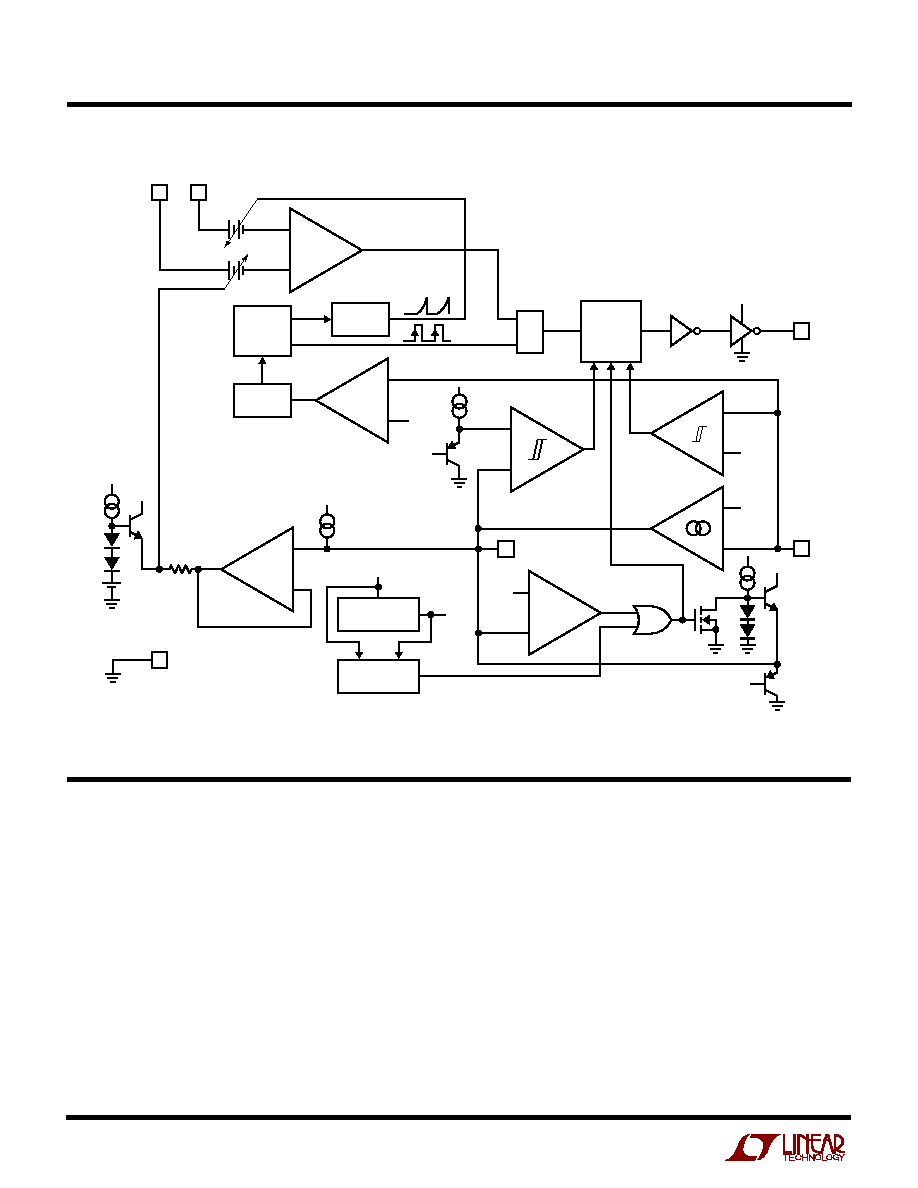
Main Control Loop
The LTC1772 is a constant frequency current mode switch-
ing regulator. During normal operation, the external
P-channel power MOSFET is turned on each cycle when
the oscillator sets the RS latch (RS1) and turned off when
the current comparator (ICMP) resets the latch. The peak
inductor current at which ICMP resets the RS latch is
controlled by the voltage on the I
TH
/RUN pin, which is the
output of the error amplifier EAMP. An external resistive
divider connected between V
OUT
and ground allows the
EAMP to receive an output feedback voltage V
FB
. When the
FU
N
CTIO
N
AL DIAGRA
U
U
W
SWITCHING
LOGIC AND
BLANKING
CIRCUIT
+
+
0.5
µ
A
0.3V
0.3V
OVP
SHORT-CIRCUIT
DETECT
SHDN
1.2V
UV
1772 FD
V
REF
+
60mV
V
REF
0.8V
V
IN
RS1
VOLTAGE
REFERENCE
SLOPE
COMP
ICMP
R
S
Q
FREQ
FOLDBACK
OSC
SENSE
V
IN
5
2
4
+
4
EAMP
V
FB
+
3
PGATE
V
IN
6
I
TH
/RUN
V
IN
0.35V
V
REF
0.8V
1
+
SHDN
CMP
GND
+
UNDERVOLTAGE
LOCKOUT
V
IN
0.15V
+
BURST
CMP
SLEEP
OPERATIO
U
(Refer to Functional Diagram)
load current increases, it causes a slight decrease in V
FB
relative to the 0.8V reference, which in turn causes the
I
TH
/RUN voltage to increase until the average inductor
current matches the new load current.
The main control loop is shut down by pulling the I
TH
/RUN
pin low. Releasing I
TH
/RUN allows an internal 0.5
µ
A
current source to charge up the external compensation
network. When the I
TH
/RUN pin reaches 0.35V, the main
control loop is enabled with the I
TH
/RUN voltage then
pulled up to its zero current level of approximately 0.7V.
As the external compensation network continues to charge
5
LTC1772
1772fs, sn1772
OPERATIO
U
(Refer to Functional Diagram)
Short-Circuit Protection
When the output is shorted to ground, the frequency of the
oscillator will be reduced to about 120kHz. This lower
frequency allows the inductor current to safely discharge,
thereby preventing current runaway. The oscillator's fre-
quency will gradually increase to its designed rate when
the feedback voltage again approaches 0.8V.
Overvoltage Protection
As a further protection, the overvoltage comparator in the
LTC1772 will turn the external MOSFET off when the
feedback voltage has risen 7.5% above the reference
voltage of 0.8V. This comparator has a typical hysteresis
of 20mV.
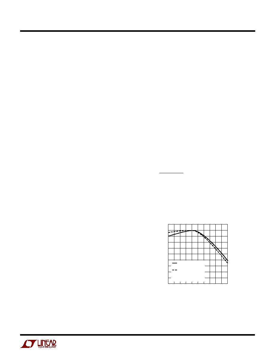
Slope Compensation and Inductor's Peak Current
The inductor's peak current is determined by:
I
V
R
PK
ITH
SENSE
=
(
)
.
0 7
10
when the LTC1772 is operating below 40% duty cycle.
However, once the duty cycle exceeds 40%, slope com-
pensation begins and effectively reduces the peak induc-
tor current. The amount of reduction is given by the curves
in Figure 2.
up, the corresponding output current trip level follows,
allowing normal operation.
Comparator OVP guards against transient overshoots
> 7.5% by turning off the external P-channel power
MOSFET and keeping it off until the fault is removed.
Burst Mode Operation
The LTC1772 enters Burst Mode operation at low load
currents. In this mode, the peak current of the inductor is
set as if V
ITH
/RUN = 1V (at low duty cycles) even though
the voltage at the I
TH
/RUN pin is at a lower value. If the
inductor's average current is greater than the load require-
ment, the voltage at the I
TH
/RUN pin will drop. When the
I
TH
/RUN voltage goes below 0.85V, the sleep signal goes
high, turning off the external MOSFET. The sleep signal
goes low when the I
TH
/RUN voltage goes above 0.925V
and the LTC1772 resumes normal operation. The next
oscillator cycle will turn the external MOSFET on and the
switching cycle repeats.
Dropout Operation
When the input supply voltage decreases towards the
output voltage, the rate of change of inductor current
during the ON cycle decreases. This reduction means that
the external P-channel MOSFET will remain on for more
than one oscillator cycle since the inductor current has not
ramped up to the threshold set by EAMP. Further reduc-
tion in input supply voltage will eventually cause the
P-channel MOSFET to be turned on 100%, i.e., DC. The
output voltage will then be determined by the input voltage
minus the voltage drop across the MOSFET, the sense
resistor and the inductor.
Undervoltage Lockout
To prevent operation of the P-channel MOSFET below safe
input voltage levels, an undervoltage lockout is incorpo-
rated into the LTC1772. When the input supply voltage
drops below approximately 2.0V, the P-channel MOSFET
and all circuitry is turned off except the undervoltage block,
which draws only several microamperes.
DUTY CYCLE (%)
0
10 20 30 40 50 60 70 80 90 100
SF = I
OUT
/I
OUT(MAX)
(%)
1772 F02
110
100
90
80
70
60
50
40
30
20
10
I
RIPPLE
= 0.4I
PK
AT 5% DUTY CYCLE
I
RIPPLE
= 0.2I
PK
AT 5% DUTY CYCLE
V
IN
= 4.2V
Figure 2. Maximum Output Current vs Duty Cycle