 | ÐлекÑÑоннÑй компоненÑ: LTC1775 | СкаÑаÑÑ:  PDF PDF  ZIP ZIP |
Äîêóìåíòàöèÿ è îïèñàíèÿ www.docs.chipfind.ru
1
LTC1775
DESCRIPTIO
U
FEATURES
APPLICATIO S
U
TYPICAL APPLICATIO
N
U
High Power
No R
SENSE
TM
Current Mode
Synchronous Step-Down
Switching Regulator
s
Highest Efficiency Current Mode Controller
s
No Sense Resistor Required
s
300mV Maximum Current Sense Voltage
s
Stable High Current Operation
s
Dual N-Channel MOSFET Synchronous Drive
s
Wide V
IN
Range: 4V to 36V
s
Wide V
OUT
Range: 1.19V to V
IN
s
±
1% 1.19V Reference
s
Programmable Fixed Frequency with Injection Lock
s
Very Low Drop Out Operation: 99% Duty Cycle
s
Forced Continuous Mode Control Pin
s
Optional Programmable Soft Start
s
Pin Selectable Output Voltage
s
Foldback Current Limit
s
Output Overvoltage Protection
s
Logic Controlled Micropower Shutdown: I
Q
< 30
µ
A
s
Available in 16-Lead Narrow SSOP and SO Packages
The LTC
®
1775 is a synchronous step-down switching
regulator controller that drives external N-channel power
MOSFETs using few external components. Current mode
control with MOSFET V
DS
sensing eliminates the need for
a sense resistor and improves efficiency. Largely similar
to the LTC1625, the LTC1775 has twice the maximum
sense voltage for high current applications. The frequency
of a nominal 150kHz internal oscillator can be synchro-
nized to an external clock over a 1.5:1 frequency range.
Burst Mode
TM
operation at low load currents reduces
switching losses and low dropout operation extends oper-
ating time in battery-powered systems. A forced continu-
ous mode control pin can assist secondary winding
regulation by disabling Burst Mode operation when the
main output is lightly loaded.
Fault protection is provided by foldback current limiting
and an output overvoltage comparator. An external ca-
pacitor attached to the RUN/SS pin provides soft start
capability for supply sequencing. A wide supply range
allows operation from 4V (4.3V for LTC1775I) to 36V at the
input and 1.19V to V
IN
at the output.
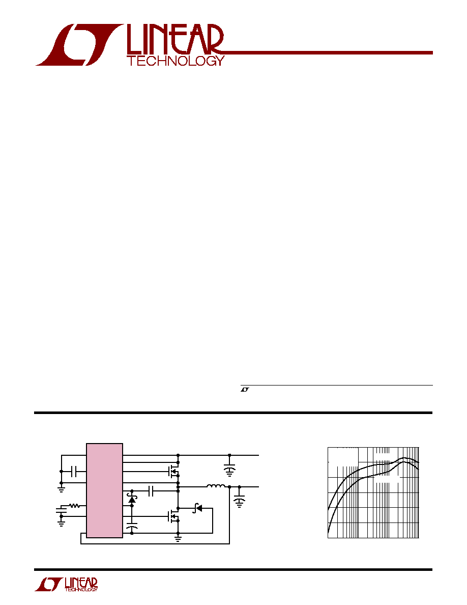
Figure 1. High Efficiency Step-Down Converter
Efficiency vs Load Current
s
Notebook Computers
s
Automotive Electronics
s
Battery Chargers
s
Distributed Power Systems
, LTC and LT are registered trademarks of Linear Technology Corporation.
No R
SENSE
and Burst Mode are trademarks of Linear Technology Corporation.
+
V
IN
TK
SYNC
LTC1775
RUN/SS
V
OSENSE
TG
SW
C
B
0.33
µ
F
D
B
CMDSH-3
C
C
2.2nF
R
C
10k
M2
SUD50N03-10
D1
MBRS340
M1
SUD50N03-10
C
VCC
4.7
µ
F
1775 F01
L1
6
µ
H
C
IN
22
µ
F
30V
×
4
BOOST
INTV
CC
BG
V
PROG
I
TH
SGND
PGND
+
C
OUT
680
µ
F
6.3V
V
OUT
3.3V
10A
V
IN
5V TO
28V
C
SS
0.1
µ
F
+
LOAD CURRENT (A)
0.01
70
EFFICIENCY (%)
90
95
100
0.1
1
10
1775 F01b
85
80
75
V
IN
= 10V
f = 150kHz
FCB = INTV
CC
V
OUT
= 5V
V
OUT
= 3.3V
2
LTC1775
(Note 1)
Input Supply Voltage (V
IN
, TK) ................. 36V to 0.3V
Boosted Supply Voltage (BOOST) ............. 42V to 0.3V
Boosted Driver Voltage (BOOST SW) ...... 7V to 0.3V
Switch Voltage (SW) ....................................36V to 5V
EXTV
CC
Voltage ...........................................7V to 0.3V
I
TH
Voltage ................................................2.7V to 0.3V
FCB, RUN/SS, SYNC Voltages .....................7V to 0.3V
V
OSENSE
, V
PROG
Voltages ........(INTV
CC
+ 0.3V) to 0.3V
Peak Driver Output Current < 10
µ
s (TG, BG) ............ 2A
INTV
CC
Output Current ........................................ 50mA
Operating Ambient Temperature Range
LTC1775C .............................................. 0
°
C to 70
°
C
LTC1775I (Note 5) .............................. 40
°
C to 85
°
C
Junction Temperature (Note 2) ............................. 125
°
C
Storage Temperature Range ................ 65
°
C to 150
°
C
Lead Temperature (Soldering, 10 sec)................. 300
°
C
SYMBOL
PARAMETER
CONDITIONS
MIN
TYP
MAX
UNITS
Main Control Loop
I
IN
V
OSENSE
Feedback Current
V
PROG
Pin Open, I
TH
= 1.19V (Note 3)
10
50
nA
V
OUT
Regulated Output Voltage
I
TH
= 1.19V (Note 3)
1.19V (Adjustable) Selected
V
PROG
Pin Open
q
1.178
1.190
1.202
V
3.3V Selected
V
PROG
= 0V
q
3.220
3.300
3.380
V
5V Selected
V
PROG
= INTV
CC
q
4.900
5.000
5.100
V
V
LINEREG
Reference Voltage Line Regulation
V
IN
= 4V to 20V, I
TH
= 1.19V (Note 3),
0.001
0.01
%/V
V
PROG
Pin Open
V
LOADREG
Output Voltage Load Regulation
I
TH
= 2V (Note 3)
q
0.020
0.2
%
I
TH
= 0.5V (Note 3)
q
0.035
0.2
%
V
FCB
Forced Continuous Threshold
V
FCB
Ramping Negative
q
1.16
1.19
1.22
V
I
FCB
Forced Continuous Bias Current
V
FCB
= 1.19V
1
2
µ
A
V
OVL
Output Overvoltage Lockout
V
PROG
Pin Open
1.24
1.28
1.32
V
I
PROG
V
PROG
Input Current
3.3V V
OUT
V
PROG
= 0V
3.5
7
µ
A
5V V
OUT
V
PROG
= 5V
3.5
7
µ
A
I
Q
Input DC Supply Current
Normal Mode
EXTV
CC
= 5V (Note 4)
500
µ
A
Shutdown
V
RUN/SS
= 0V, 4V < V
IN
< 15V
15
30
µ
A
V
RUN/SS
RUN/SS Pin Threshold
q
0.8
1.4
2
V
I
RUN/SS
Soft Start Current Source
V
RUN/SS
= 0V
1.2
2.5
4
µ
A
V
SENSE(MAX)
Maximum Current Sense Threshold
V
OSENSE
= 1V, V
PROG
Pin Open
260
300
340
mV
ORDER PART
NUMBER
LTC1775CGN
LTC1775CS
LTC1775IGN
LTC1775IS
Consult factory for Military grade parts.
T
JMAX
= 125
°
C,
JA
= 130
°
C/W (GN)
T
JMAX
= 125
°
C,
JA
= 110
°
C/W (S)
The
q
denotes specifications which apply over the full operating temperature
range, otherwise specifications are at T
A
= 25
°
C. V
IN
= 15V unless otherwise noted.
TOP VIEW
S PACKAGE
16-LEAD PLASTIC SO
GN PACKAGE
16-LEAD NARROW
PLASTIC SSOP
1
2
3
4
5
6
7
8
16
15
14
13
12
11
10
9
EXTV
CC
SYNC
RUN/SS
FCB
I
TH
SGND
V
OSENSE
V
PROG
V
IN
TK
SW
TG
BOOST
INTV
CC
BG
PGND
GN PART MARKING
1775
1775I
ABSOLUTE AXI U RATI GS
W
W
W
U
PACKAGE/ORDER I FOR ATIO
U
U
W
ELECTRICAL CHARACTERISTICS
3
LTC1775
Note 1: Absolute Maximum Ratings are those values beyond which the life
of a device may be impaired.
Note 2: T
J
is calculated from the ambient temperature T
A
and power
dissipation P
D
according to the following formula:
LTC1775CGN/LTC1775IGN: T
J
= T
A
+ (P
D
· 130
°
C/W)
LTC1775CS/LTC1775IS: T
J
= T
A
+ (P
D
· 110
°
C/W)
Note 3: The LTC1775 is tested in a feedback loop that adjusts V
OSENSE
to
achieve a specified error amplifier output voltage (I
TH
).
Note 4: Typical in application circuit with EXTV
CC
tied to V
OUT
= 5V,
I
OUT
= 0A and FCB = INTV
CC
. Dynamic supply current is higher due
to the gate charge being delivered at the switching frequency. See
Applications Information.
Note 5: Minimum input supply voltage is 4.3V at 40
°
C for industrial
grade parts.
Note 6: Rise and fall times are measured at 10% to 90% levels.
The
q
denotes specifications which apply over the full operating temperature
range, otherwise specifications are at T
A
= 25
°
C. V
IN
= 15V unless otherwise noted.
SYMBOL
PARAMETER
CONDITIONS
MIN
TYP
MAX
UNITS
TG Transition Time
(Note 6)
TG t
R
Rise Time
C
LOAD
= 3300pF
50
150
ns
TG t
F
Fall Time
C
LOAD
= 3300pF
50
150
ns
BG Transition Time
(Note 6)
BG t
R
Rise Time
C
LOAD
= 3300pF
50
150
ns
BG t
F
Fall Time
C
LOAD
= 3300pF
50
150
ns
Internal V
CC
Regulator
V
INTVCC
Internal V
CC
Voltage
6V < V
IN
< 30V, V
EXTVCC
= 4V
q
5.0
5.2
5.4
V
V
LDOINT
INTV
CC
Load Regulation
I
CC
= 20mA, V
EXTVCC
= 4V
0.2
1
%
V
LDOEXT
EXTV
CC
Voltage Drop
I
CC
= 20mA, V
EXTVCC
= 5V
180
300
mV
V
EXTVCC
EXTV
CC
Switchover Voltage
I
CC
= 20mA, V
EXTVCC
Ramping Positive
q
4.5
4.7
V
Oscillator
f
OSC
Oscillator Freqency
SYNC = 0V
135
150
165
kHz
f
H
/f
OSC
Maximum Synchronized Frequency Ratio
1.5
V
SYNC
SYNC Pin Threshold (Figure 4)
Ramping Positive
0.9
1.2
V
R
SYNC
SYNC Pin Input Resistance
50
k
ELECTRICAL CHARACTERISTICS
4
LTC1775
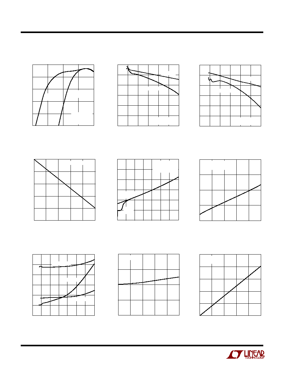
LOAD CURRENT (A)
0.001
EFFICIENCY (%)
10
1775 · G01
0.01
0.1
1.0
100
90
80
70
60
50
CONTINUOUS
MODE
BURST
MODE
V
IN
= 10V
V
OUT
= 5V
EXTV
CC
= V
OUT
INPUT VOLTAGE (V)
0
EFFICIENCY (%)
100
95
90
85
80
75
70
5
10
15
20
1775 · G02
25
30
I
LOAD
= 5A
I
LOAD
= 500mA
V
OUT
= 5V
FIGURE 1 CIRCUIT
INPUT VOLTAGE (V)
0
5
10
15
20
25
30
100
95
90
85
80
75
70
1775 · G03
EFFICIENCY (%)
I
LOAD
= 5A
I
LOAD
= 500mA
V
OUT
= 3.3V
FIGURE 1 CIRCUIT
LOAD CURRENT (A)
0
V
OUT
(%)
0
0.1
0.2
0.3
0.4
0.5
8
1775 · G04
2
4
6
10
FIGURE 1 CIRCUIT
CURRENT LOAD (A)
0
V
IN
V
OUT
(mV)
10
1775 · G06
2
4
6
8
400
300
200
100
0
FIGURE 1 CIRCUIT
V
OUT
= 5V, 5% DROP
LOAD CURRENT (A)
0
V
ITH
(V)
3.0
2.5
2.0
1.5
1.0
0.5
0
6
10
1775 · G05
2
4
8
12
14
FIGURE 1 CIRCUIT
V
IN
= 20V
V
OUT
= 5V
CONTINUOUS
MODE
BURST
MODE
INTV
CC
LOAD CURRENT (mA)
0
EXTV
CC
INTV
CC
(mV)
500
400
300
200
100
0
40
1775 · G09
10
20
30
50
V
IN
= 15V
EXTV
CC
= 5V
INPUT VOLTAGE (V)
0
INPUT CURRENT (
µ
A)
SHUTDOWN CURRENT (
µ
A)
1200
1000
800
600
400
200
0
15
25
1775 · G07
5
10
20
30
35
60
50
40
30
20
10
0
EXTV
CC
= 5V
SHUTDOWN
EXTV
CC
OPEN
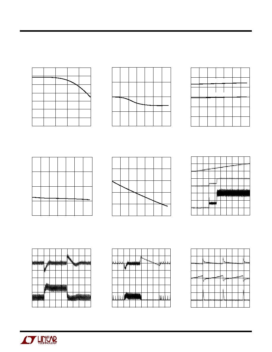
Efficiency vs Load Current
Efficiency vs Input Voltage
Efficiency vs Input Voltage
Load Regulation
V
IN
V
OUT
Dropout Voltage
vs Load Current
I
TH
Pin Voltage vs Load Current
Input and Shutdown Current
vs Input Voltage
INTV
CC
Load Regulation
EXTV
CC
Switch Drop
vs INTV
CC
Load Current
INTV
CC
LOAD CURRENT (mA)
0
INTV
CC
(%)
50
1775 · G08
10
20
30
40
1.0
0.5
0
0.5
1.0
V
IN
= 15V
TYPICAL PERFOR A CE CHARACTERISTICS
U
W
5
LTC1775
DUTY CYCLE
0
350
300
250
200
150
100
50
0
0.6
1775 · G10
0.2
0.4
0.8
1.0
MAXIMUM CURRENT SENSE VOLTAGE (mV)
TEMPERATURE (
°
C)
40
MAXIMUM CURRENT SENSE VOLTAGE (mV)
320
310
300
290
280
35
85
1775 · G11
15
10
60
110
135
TEMPERATURE (
°
C)
40
FREQUENCY (kHz)
300
250
200
150
100
50
0
35
85
1775 · G12
15
10
60
110
135
SYNC = 1.5V
SYNC = 0V
Maximum Current Sense Voltage
vs Duty Cycle
Maximum Current Sense Voltage
vs Temperature
Oscillator Frequency
vs Temperature
1530 G15
V
OUT
50mV
/DIV
I
TH
100mV
/DIV
I
L
2A/DIV
V
IN
= 20V
V
OUT
= 5V
I
LOAD
= 100mA
FIGURE 1 CIRCUIT
20
µ
s/DIV
FCB Pin Current vs Temperature
RUN/SS Pin Current vs
Temperature
Burst Mode Operation
TEMPERATURE (
°
C)
40
FCB CURRENT (
µ
A)
35
85
1775 · G13
15
10
60
110
135
0
0.5
1.0
1.5
2.0
TEMPERATURE (
°
C)
40
RUN/SS CURRENT (
µ
A)
0
1
2
3
4
5
35
85
1775 · G14
15
10
60
110
135
Soft Start
1530 G16
RUN/SS
5V/DIV
V
OUT
5V/DIV
I
L
5A/DIV
V
IN
= 20V
V
OUT
= 5V
R
LOAD
= 0.5
FIGURE 1 CIRCUIT
20ms/DIV
1530 G17
V
OUT
100mV
/DIV
I
L
5A/DIV
V
IN
= 20V
V
OUT
= 5V
I
LOAD
= 100mA TO 2A
FIGURE 1 CIRCUIT
200
µ
s/DIV
1530 G18
V
OUT
100mV
/DIV
I
L
5A/DIV
V
IN
= 20V
V
OUT
= 5V
I
LOAD
= 2A TO 8A
FIGURE 1 CIRCUIT
100
µ
s/DIV
Transient Response
(Burst Mode Operation)
Transient Response
TYPICAL PERFOR A CE CHARACTERISTICS
U
W