Äîêóìåíòàöèÿ è îïèñàíèÿ www.docs.chipfind.ru
1
LTC1841/LTC1842/LTC1843
Ultralow Power Dual
Comparators with Reference
LTC1843 Supply Current
vs Supply Voltage
SUPPLY VOLTAGE (V)
0
SUPPLY CURRENT (
µ
A)
3
4
5
8
1841/43 TA02
2
1
0
2
4
6
10
12
T
A
= 25
°
C
The LTC
®
1841/LTC1842/LTC1843 are ultralow power dual
comparators with built-in reference (LTC1842/LTC1843).
The comparators feature less than 5.7
µ
A supply current
over temperature, a 1.182V
±
1% reference, program-
mable hysteresis and open-drain outputs that sink cur-
rent. The reference output can drive a bypass capacitor of
up to 0.01
µ
F without oscillation.
The LTC1841 operates from a single 2V to 11V supply or
a dual
±
1V to
±
5.5V supply. The LTC1842/LTC1843
operate from a single 2.5V to 11V supply or a dual
±
1.25V
to
±
5.5V supply. The LTC1842/LTC1843 hysteresis is
easily programmed by using two resistors and the HYST
pin. The comparators' input operates from the negative
supply to within 1.3V of the positive supply. The compara-
tors' output stage can typically sink greater than 20mA. By
eliminating the cross-conduction current that normally
happens when the comparators change logic states, power
supply glitches are eliminated.
The LTC1841/LTC1842/LTC1843 are available in SO-8
packages.
FEATURES
DESCRIPTIO
N
U
s
Ultralow Quiescent Current: 3.5
µ
A Typ
s
Open-Drain Outputs Typically Sink
Greater Than 20mA
s
Wide Supply Range: (LTC1841)
Single: 2V to 11V
Dual:
±
1V to
±
5.5V
s
Input Voltage Range Includes the Negative Supply
s
Reference Output Drives 0.01
µ
F Capacitor
s
Adjustable Hysteresis
s
12
µ
s Propagation Delay with 10mV Overdrive
s
No Current Spike When Switching
R4
20k
R
C
20k
C
C
0.0
µ
F
R7
500k
OUTPUT
5V
600mA
LBO
R5
1.1M
R3
1M
R2
100k
R1
1.5M
C1
100
µ
F
1-CELL
Li-Ion
BATTERY
R6
25k
7
8
6
7
D1
L1
10
µ
H
4
8
3
1
2
1
6
C1, C2: SANYO OS-CON
D1: MOTOROLA MBRS130LT3
L1: COILTRONICS CTX10-3
2
5
1841/43 TA01
3
4
+
C2
100
µ
F
Si9924DY
+
+
+
V
CC
OUT B
LTC1843
OUT A
REF
V
HYST
IN A
+
IN B
V
IN
SW
LT1302-5
SHDN
PGND
I
T
SENSE
V
C
GND
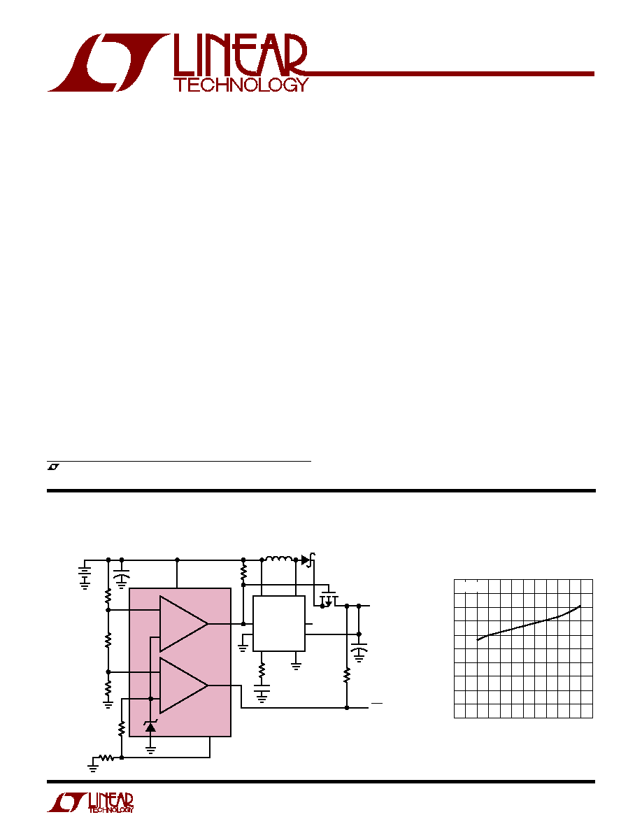
TYPICAL APPLICATIO
N
U
Single Li-Ion Cell to 5V Supply
, LTC and LT are registered trademarks of Linear Technology Corporation.
APPLICATIO
N
S
U
s
Battery-Powered System Monitoring
s
Threshold Detectors
s
Window Comparators
s
Oscillator Circuits
2
LTC1841/LTC1842/LTC1843
ABSOLUTE
M
AXI
M
U
M
RATINGS
W
W
W
U
(Note 1)
Voltage
V
+
to V
................................................12V to 0.3V
IN
+
, IN
, HYST ................. (V
+
+ 0.3V) to (V
0.3V)
REF ................................... (V
+
+ 0.3V) to (V
0.3V)
OUT ................................................ 12V to (V
0.3V)
Current
IN
+
, IN
, HYST ................................................. 20mA
REF ................................................................... 20mA
OUT .................................................................. 50mA
OUT Short-Circuit Duration (V
+
5.5V) ...... Continuous
Power Dissipation ............................................. 500mW
Operating Temperature Range
LTC1841C/LTC1842C/LTC1843C ........... 0
°
C to 70
°
C
LTC1841I/LTC1842I/LTC1843I .......... 40
°
C to 85
°
C
Storage Temperature Range ................ 65
°
C to 150
°
C
Lead Temperature (Soldering, 10 sec).................. 300
°
C
PACKAGE/ORDER I
N
FOR
M
ATIO
N
W
U
U
1
2
3
4
8
7
6
5
TOP VIEW
OUT A
V
IN A
+
IN A
OUT B
V
+
IN B
+
IN B
S8 PACKAGE
8-LEAD PLASTIC SO
1841
1841I
S8 PART
MARKING
1
2
3
4
8
7
6
5
TOP VIEW
OUT A
V
IN A
+
IN B
+
OUT B
V
+
REF
HYST
S8 PACKAGE
8-LEAD PLASTIC SO
1
2
3
4
8
7
6
5
TOP VIEW
OUT A
V
IN A
+
IN B
OUT B
V
+
REF
HYST
S8 PACKAGE
8-LEAD PLASTIC SO
T
JMAX
= 150
°
C,
JA
= 125
°
C/ W
T
JMAX
= 150
°
C,
JA
= 125
°
C/ W
T
JMAX
= 150
°
C,
JA
= 125
°
C/ W
ORDER PART
NUMBER
LTC1841CS8
LTC1841IS8
S8 PART
MARKING
ORDER PART
NUMBER
S8 PART
MARKING
1842
1842I
LTC1842CS8
LTC1842IS8
ORDER PART
NUMBER
LTC1843CS8
LTC1843IS8
1843
1843I
ELECTRICAL CHARACTERISTICS
V
+
= 5V, V
= 0V, T
A
= 25
°
C unless otherwise noted.
Consult factory for Military grade parts.
SYMBOL PARAMETER
CONDITIONS
MIN
TYP
MAX
UNITS
Power Supply
V
+
Supply Voltage Range
LTC1841
q
2.0
11
V
LTC1842/LTC1843
q
2.5
11
V
I
CC
Supply Current
HYST = REF (Note 2)
q
3.5
5.7
µ
A
Comparator
V
OS
Comparator Input Offset Voltage
(Note 3)
q
±
3
±
10
mV
I
IN
Input Leakage Current (IN
+
, IN
)
IN
+
= IN
= 2.5V (LTC1841),
q
±
0.01
±
1.0
nA
IN
+
= IN
= V
REF
(LTC1842/LTC1843)
V
IN
Comparator Input Voltage Range
q
V
V
+
1.3V
V
PSRR
Power Supply Rejection Ratio
V
+
= 2V to 11V (LTC1841),
0.1
1
mV/V
V
+
= 2.5V to 11V (LTC1842/LTC1843)
CMRR
Common Mode Rejection Ratio
V
CM
= V
to (V
+
1.3V) LTC1841
q
0.1
1
mV/V
V
HYST
Hysteresis Input Voltage Range
LTC1842/LTC1843
q
V
REF
50mV
V
REF
V

3
LTC1841/LTC1842/LTC1843
ELECTRICAL CHARACTERISTICS
V
+
= 5V, V
= 0V, T
A
= 25
°
C unless otherwise noted.
SYMBOL PARAMETER
CONDITIONS
MIN
TYP
MAX
UNITS
t
PD
Propagation Delay
C
OUT
= 10pF, R
PULL-UP
= 100k
Overdrive = 10mV
12
µ
s
Overdrive = 100mV
4
µ
s
I
LEAK
Output Leakage Current
V
OUT
= 12V (Note 2)
q
1
100
nA
V
OL
Output Low Voltage
I
OUT
= 1.8mA
q
V
+ 0.4V
V
Reference (LTC1842/LTC1843)
V
REF
Reference Voltage
No Load
25
°
C
1.174
1.182
1.190
V
0
°
C to 70
°
C
q
1.170
1.194
V
40
°
C to 85
°
C
q
1.164
1.200
V
V
REF
Load Regulation
I
SOURCE
= 1mA
q
1
3
mV
I
SINK
=10
µ
A
1.75
4
mV
q
6
mV
e
n
Voltage Noise
100Hz to 100kHz
100
µ
V
RMS
V
+
= 3V, V
= 0V, T
A
= 25
°
C unless otherwise noted.
SYMBOL PARAMETER
CONDITIONS
MIN
TYP
MAX
UNITS
Power Supply
V
+
Supply Voltage Range
LTC1841
q
2.0
11
V
LTC1842/LTC1843
q
2.5
11
V
I
CC
Supply Current
HYST = REF (Note 2)
q
3.5
5.5
µ
A
Comparator
V
OS
Comparator Input Offset Voltage
(Note 3)
q
±
3
±
10
mV
I
IN
Input Leakage Current (IN
+
, IN
)
IN
+
= IN
= 1.5V (LTC1841),
q
±
0.01
±
1
nA
IN
+
= IN
= V
REF
(LTC1842/LTC1843)
V
IN
Comparator Input Voltage Range
q
V
V
+
1.3V
V
PSRR
Power Supply Rejection Ratio
V
+
= 2V to 11V (LTC 1841),
0.1
1
mV/V
V
+
= 2.5V to 11V (LTC1842/LTC1843)
CMRR
Common Mode Rejection Ratio
V
CM
= V
to (V
+
1.3V) LTC1841
q
0.1
1
mV/V
V
HYST
Hysteresis Input Voltage Range
LTC1842/LTC1843
q
V
REF
50mV
V
REF
V
t
PD
Propagation Delay
C
OUT
= 10pF, R
PULL-UP
= 100k
Overdrive = 10mV
14
µ
s
Overdrive = 100mV
5
µ
s
I
LEAK
Output Leakage Current
V
OUT
= 12V (Note 2)
q
1
100
nA
V
OL
Output Low Voltage
I
O
= 0.8mA
q
V
+ 0.4V
V
Reference (LTC1842/LTC1843)
V
REF
Reference Voltage
No Load
25
°
C
1.174
1.182
1.190
V
0
°
C to 70
°
C
q
1.170
1.194
V
40
°
C to 85
°
C
q
1.164
1.200
V
V
REF
Load Regulation
I
SOURCE
= 1mA
q
2
6
mV
I
SINK
=10
µ
A
1.75
4
mV
q
6
mV
e
n
Voltage Noise
100Hz to 100kHz
100
µ
V
RMS
The
q
denotes specifications which apply over the full operating
temperature range.
Note 1: Absolute Maximum Ratings are those values beyond which the life
of a device may be impaired.
Note 2: IN
+
= IN
+ 80mV, output is in high impedance state.
Note 3: V
CM
= 1/2(V
+
V
) for LTC1841, V
CM
= V
REF
for LTC1842/
LTC1843.

4
LTC1841/LTC1842/LTC1843
TYPICAL PERFOR
M
A
N
CE CHARACTERISTICS
U
W
Comparator Response Time vs
Input Overdrive, with R
PULL-UP
= 5k
Comparator Response Time vs
Input Overdrive, with R
PULL-UP
= 5k
RESPONSE TIME (
µ
s)
1
INPUT VOLTAGE (mV)
OUTPUT VOLTAGE (V)
0
0
1
6
14
18
5
1440/1/2/3 G02
100
2
10
4
12
16
0
8
2
3
4
100mV
10mV
50mV
20mV
T
A
= 25
°
C
Comparator Short-Circuit Sink
Current vs Supply Voltage
SUPPLY VOLTAGE (V)
0
SINK CURRENT (mA)
200
180
160
140
120
100
80
60
40
20
0
8
1440/1/2/3 G03
2
1
3
5
7
9
4
6
10
OUT CONNECTED TO V
+
T
A
= 25
°
C
Comparator Response Time vs
Load Capacitance with 100mV
Input Overdrive
LOAD CAPACITANCE (nF)
0
RESPONSE TIME (
µ
s)
12
10
8
6
4
2
80
1440/1/2/3 G04
20
40
60
100
t
PHL
t
PLH
Comparator Response Time at
Low Supply Voltage
SUPPLY VOLTAGE (V)
1.0
RESPONSE TIME (
µ
s)
10000
1000
100
10
1
1.2
1.4
1.6
1.1
1.3
1.5
1440/1/2/3 G05
20mV OVERDRIVE
100mV OVERDRIVE
Comparator Output Voltage Low
vs Load Current
LOAD CURRENT (mA)
0
OUTPUT VOLTAGE HIGH (V)
1.5
2.0
2.5
30
50
80
1440/1/2/3 G06
1.0
0.5
0
10
20
40
60
70
V
+
= 2V
V
+
= 3V
V
+
= 5V
T
A
= 25
°
C
RESPONSE TIME (
µ
s)
1
INPUT VOLTAGE (mV)
OUTPUT VOLTAGE (V)
100
0
1
6
4
5
1440/1/2/3 G01
0
2
0
10
8
2
3
4
100mV
10mV
50mV
20mV
T
A
= 25
°
C
5
LTC1841/LTC1842/LTC1843
TYPICAL PERFOR
M
A
N
CE CHARACTERISTICS
U
W
LTC1842/LTC1843
Hysteresis Control
LTC1842/LTC1843
Supply Current vs Temperature
V
REF
V
HYST
(mV)
0
POSITIVE-TO-NEGATIVE INPUT VOLTAGE (mV)
30
50
1440/1/2/3 G07
10
20
40
80
60
40
20
0
20
40
60
80
OUTPUT HIGH
OUTPUT LOW
TEMPERATURE (
°
C)
60
SUPPLY CURRENT (
µ
A)
4.5
4.0
3.5
3.0
2.5
2.0
100
1440/1/2/3 G08
20
40
20 40
80
120
0
60
140
V
+
= 5V
V
= 5V
V
+
= 5V
V
= 0V
V
+
= 3V
V
= 0V
OUTPUT LOAD CURRENT (mA)
0
1.190
1.185
1.180
1.175
1.170
1.165
1.160
1.155
1.5
2.5
1841/2/3 G09
0.5
1.0
2.0
3.0
3.5
REFERENCE OUTPUT VOLTAGE (V)
V
CC
= 5V
SOURCE
Reference Output Voltage vs
Output Load Current
Reference Output Voltage vs Output
Load Current (Sink)
OUTPUT LOAD CURRENT (
µ
A)
0
REFERENCE OUTPUT VOLTAGE (V)
1.200
1.195
1.190
1.185
1.180
1.175
1.170
5
10
15
20
1440/1/2/3 G10
25
30
V
CC
= 5V
SINK
V
CC
= 2V
TEMPERATURE (
°
C)
60
REFERENCE VOLTAGE (V)
1.186
1.184
1.182
1.180
1.178
1.176
1.174
1.172
1.170
100
1440/1/2/3 G11
20
40
20 40
80
120
0
60
140
Reference Voltage vs
Temperature