Äîêóìåíòàöèÿ è îïèñàíèÿ www.docs.chipfind.ru
1
LTC1844 Series
1844ia
150mA, Micropower,
Low Noise, VLDO
Linear Regulator
May 2003
s
Very Low Dropout:
90mV at 150mA
30mV at 50mA (LTC1844-3.3)
s
Wide Input Voltage Range: 1.6V to 6.5V
s
Low 35
µ
A Supply Current, Even in Dropout
s
Low Noise: 30
µ
V
RMS
(10Hz to 100kHz)
s
±
1.75% Voltage Accuracy Over Temperature,
Voltage and Current Ranges
s
Fast Transient Response
s
10nA Supply Current in Shutdown
s
Fixed Output Voltages: 1.5V, 1.8V, 2.5V, 2.8V, 3.3V
s
Adjustable Output Voltage: 1.25V to 6V
s
Output Current Limit
s
Reverse-Battery and Reverse-Current Protection
s
No Protection Diodes Needed
s
Stable with 1
µ
F Output Capacitor
s
Stable with Ceramic Capacitors
s
Short-Circuit and Thermal Overload Protection
s
Low Profile (1mm) SOT-23 Package
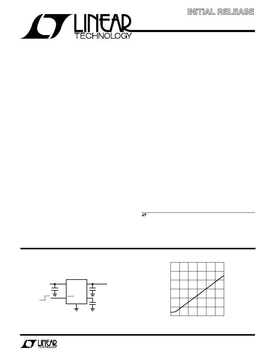
Fixed Voltage Low Noise, VLDO Linear Regulator
s
Bluetooth/802.11 Cards
s
PDAs and Notebook Computers
s
Portable Instruments and Battery-Powered Systems
s
Cellular Phones
FEATURES
DESCRIPTIO
U
APPLICATIO S
U
TYPICAL APPLICATIO
U
The LTC
®
1844 Series are low noise VLDO
TM
(very low
dropout) linear regulators designed for low power/portable
applications. These regulators can operate from input
voltages as low as 1.6V. Typical output noise is only
30
µ
V
RMS
and typical dropout for the LTC1844-3.3 is just
90mV at the maximum load current of 150mA, reducing to
30mV at 50mA.
The internal P-channel MOSFET pass transistor requires
no base current, allowing the device to draw only 35
µ
A
during normal operation, independent of the dropout
voltage and load current. The quiescent current falls to a
negligible 10nA during shutdown.
Other features include high output voltage accuracy,
excellent transient response, stablity with ultralow ESR
ceramic capacitors as small as 1
µ
F, reverse-battery and
reverse-current protection, short-circuit and thermal
overload protection and output current limiting.
The LTC1844 regulators are available in a low profile
(1mm) SOT-23 (ThinSOT
TM
) package.
, LTC and LT are registered trademarks of Linear Technology Corporation.
Final Electrical Specifications
Information furnished by Linear Technology Corporation is believed to be accurate and reliable.
However, no responsibility is assumed for its use. Linear Technology Corporation makes no represen-
tation that the interconnection of its circuits as described herein will not infringe on existing patent rights.
IN
SHDN
1844 TA01
1
µ
F
LTC1844-3.3
OUT
V
OUT
3.3V
V
IN
3.3V TO 6.5V
BYP
GND
0.1
µ
F
1
µ
F
OFF ON
5
4
2
3
1
VLDO and ThinSOT are trademarks of Linear Technology Corporation.
LTC1844-3.3 Dropout Voltage vs Load Current
I
OUT
(mA)
0
0
DROPOUT VOLTAGE (mV)
20
40
60
80
120
100
25
50
75
100
1844 TA02
125
150
2
LTC1844 Series
1844ia
(Note 1)
Supply Voltage (IN) ....................................... 7V to 7V
Input Voltage
SHDN, BYP, ADJ .................................... 0.3V to 7V
Output Voltage
OUT ........................................................ 0.3V to 7V
OUT to IN .................................................. 7V to 7V
ABSOLUTE AXI U RATI GS
W
W
W
U
ELECTRICAL CHARACTERISTICS
SYMBOL
PARAMETER
CONDITIONS
MIN
TYP
MAX
UNITS
V
IN
Input Voltage
q
1.6
6.5
V
I
IN
Quiescent Current
SHDN = V
IN
35
55
µ
A
q
80
µ
A
I
INSHDN
V
IN
Shutdown Supply Current
SHDN = 0V
q
0.01
1
µ
A
V
OUT%
Regulated Output Voltage
LTC1844-3.3
V
IN
= 3.8V to 6.5V, I
OUT
= 0mA to 150mA
1.50
1.50
%V
OUT
(Notes 3, 4, 5)
LTC1844-3.3
V
IN
= 3.8V to 6.5V, I
OUT
= 0mA to 150mA
q
1.75
1.75
%V
OUT
LTC1844-2.8
V
IN
= 3.3V to 6.5V, I
OUT
= 0mA to 150mA
1.50
1.50
%V
OUT
LTC1844-2.8
V
IN
= 3.3V to 6.5V, I
OUT
= 0mA to 150mA
q
1.75
1.75
%V
OUT
LTC1844-2.5
V
IN
= 3.0V to 6.5V, I
OUT
= 0mA to 150mA
1.50
1.50
%V
OUT
LTC1844-2.5
V
IN
= 3.0V to 6.5V, I
OUT
= 0mA to 150mA
q
1.75
1.75
%V
OUT
LTC1844-1.8
V
IN
= 2.3V to 6.5V, I
OUT
= 0mA to 150mA
1.50
1.50
%V
OUT
LTC1844-1.8
V
IN
= 2.3V to 6.5V, I
OUT
= 0mA to 150mA
q
1.75
1.75
%V
OUT
The
q
denotes specifications which apply over the full operating
temperature range, otherwise specifications are at T
A
= 25
°
C. V
IN
= V
OUT
+ 0.5V, unless otherwise noted. (Note 2)
Output Short-Circut Duration .......................... Indefinite
Operating Junction Temperature Range
(Notes 2, 10) .....................................40
°
C to 125
°
C
Storage Temperature Range ................. 65
°
C to 150
°
C
Lead Temperature (Soldering, 10 sec).................. 300
°
C
PACKAGE/ORDER I FOR ATIO
U
U
W
LTC1844ES5-1.5
LTC1844ES5-1.8
LTC1844ES5-2.5
LTC1844ES5-2.8
LTC1844ES5-3.3
ORDER PART
NUMBER
T
JMAX
= 150
°
C,
JA
= 250
°
C/ W,
JC
= 90
°
C/ W
SEE THE APPLICATIONS INFORMATION SECTION
S5 PART
MARKING
LTF1
LTF2
LTF3
LTQK
LTF4
5 OUT
4 BYP
IN 1
GND 2
TOP VIEW
S5 PACKAGE
5-LEAD PLASTIC TSOT-23
SHDN 3
Consult LTC Marketing for parts specified with wider operating temperature ranges.
T
JMAX
= 150
°
C,
JA
= 250
°
C/ W,
JC
= 90
°
C/ W
SEE THE APPLICATIONS INFORMATION SECTION
T
JMAX
= 150
°
C,
JA
= 250
°
C/ W,
JC
= 90
°
C/ W
SEE THE APPLICATIONS INFORMATION SECTION
LTC1844ES5-SD
ORDER PART
NUMBER
S5 PART
MARKING
LTE8
LTC1844ES5-BYP
ORDER PART
NUMBER
S5 PART
MARKING
LTE9
5 OUT
4 ADJ
IN 1
GND 2
TOP VIEW
S5 PACKAGE
5-LEAD PLASTIC TSOT-23
SHDN 3
5 OUT
4 ADJ
IN 1
GND 2
TOP VIEW
S5 PACKAGE
5-LEAD PLASTIC TSOT-23
BYP 3
3
LTC1844 Series
1844ia
SYMBOL
PARAMETER
CONDITIONS
MIN
TYP
MAX
UNITS
LTC1844-1.5
V
IN
= 2.0V to 6.5V, I
OUT
= 0mA to 150mA
1.50
1.50
%V
OUT
LTC1844-1.5
V
IN
= 2.2V to 6.5V, I
OUT
= 0mA to 150mA
q
2.00
2.00
%V
OUT
LTC1844-1.5
V
IN
= 2.0V to 6.5V, I
OUT
= 0mA to 150mA
q
2.50
2.00
%V
OUT
LTC1844-BYP
V
IN
= 1.75V to 6.5V, I
OUT
= 0mA to 150mA
1.50
1.50
%V
OUT
LTC1844-BYP
V
IN
= 2.2V to 6.5V, I
OUT
= 0mA to 150mA
q
1.75
1.75
%V
OUT
LTC1844-BYP
V
IN
= 1.75V to 6.5V, I
OUT
= 0mA to 150mA
q
3.50
1.75
%V
OUT
LTC1844-SD
V
IN
= 1.75V to 6.5V, I
OUT
= 0mA to 150mA
1.50
1.50
%V
OUT
LTC1844-SD
V
IN
= 2.2V to 6.5V, I
OUT
= 0mA to 150mA
q
1.75
1.75
%V
OUT
LTC1844-SD
V
IN
= 1.75V to 6.5V, I
OUT
= 0mA to 150mA
q
3.50
1.75
%V
OUT
V
LNR
Line Regulation (Notes 3, 5)
LTC1844-3.3
V
IN
= 3.4V to 6.5V, I
L
= 1mA
q
4
20
mV
LTC1844-2.8
V
IN
= 2.9V to 6.5V, I
L
= 1mA
q
4
20
mV
LTC1844-2.5
V
IN
= 2.6V to 6.5V, I
L
= 1mA
q
4
20
mV
LTC1844-1.8
V
IN
= 2.2V to 6.5V, I
L
= 1mA
q
4
20
mV
V
IN
= 1.9V to 6.5V, I
L
= 1mA
4
20
mV
V
IN
= 1.9V to 6.5V, I
L
= 1mA
q
4
30
mV
LTC1844-1.5
V
IN
= 2.2V to 6.5V, I
L
= 1mA
q
4
20
mV
V
IN
= 1.6V to 6.5V, I
L
= 1mA
4
20
mV
V
IN
= 1.6V to 6.5V, I
L
= 1mA
q
4
80
mV
LTC1844-BYP
V
IN
= 2.2V to 6.5V, I
L
= 1mA
q
4
20
mV
V
IN
= 1.6V to 6.5V, I
L
= 1mA
4
20
mV
V
IN
= 1.6V to 6.5V, I
L
= 1mA
q
4
80
mV
LTC1844-SD
V
IN
= 2.2V to 6.5V, I
L
= 1mA
q
4
20
mV
V
IN
= 1.6V to 6.5V, I
L
= 1mA
4
20
mV
V
IN
= 1.6V to 6.5V, I
L
= 1mA
q
4
80
mV
V
LDR
Load Regulation (Notes 3, 5)
LTC1844-3.3
V
IN
= 3.8V, I
OUT
= 0mA to 150mA
q
9
20
mV
LTC1844-2.8
V
IN
= 3.3V, I
OUT
= 0mA to 150mA
q
9
20
mV
LTC1844-2.5
V
IN
= 3.0V, I
OUT
= 0mA to 150mA
q
9
20
mV
LTC1844-1.8
V
IN
= 2.3V, I
OUT
= 0mA to 150mA
q
9
20
mV
LTC1844-1.5
V
IN
= 2.2V, I
OUT
= 0mA to 150mA
q
9
20
mV
V
IN
= 2.0V, I
OUT
= 0mA to 150mA
q
9
40
mV
LTC1844-BYP
V
IN
= 2.2V, I
OUT
= 0mA to 150mA
q
9
20
mV
V
IN
= 1.75V, I
OUT
= 0mA to 150mA
q
9
50
mV
LTC1844-SD
V
IN
= 2.2V, I
OUT
= 0mA to 150mA
q
9
20
mV
V
IN
= 1.75V, I
OUT
= 0mA to 150mA
q
9
50
mV
V
DO
Dropout Voltage (Notes 6, 7)
LTC1844-3.3
I
OUT
= 50mA
q
30
55
mV
I
OUT
= 150mA
q
90
150
mV
LTC1844-2.8
I
OUT
= 50mA
q
35
60
mV
I
OUT
= 150mA
q
105
165
mV
LTC1844-2.5
I
OUT
= 50mA
q
45
75
mV
I
OUT
= 150mA
q
135
200
mV
LTC1844-1.8
I
OUT
= 50mA
q
85
120
mV
I
OUT
= 150mA
q
230
300
mV
LTC1844-1.5
I
OUT
= 50mA
q
115
160
mV
I
OUT
= 150mA
q
350
450
mV
LTC1844-BYP
I
OUT
= 50mA
q
45
75
mV
I
OUT
= 150mA
q
135
200
mV
LTC1844-SD
I
OUT
= 50mA
q
45
75
mV
I
OUT
= 150mA
q
135
200
mV
ELECTRICAL CHARACTERISTICS
The
q
denotes specifications which apply over the full operating
temperature range, otherwise specifications are at T
A
= 25
°
C. V
IN
= V
OUT
+ 0.5V, unless otherwise noted. (Note 2)
4
LTC1844 Series
1844ia
ELECTRICAL CHARACTERISTICS
The
q
denotes specifications which apply over the full operating
temperature range, otherwise specifications are at T
A
= 25
°
C. V
IN
= V
OUT
+ 0.5V, unless otherwise noted. (Note 2)
SYMBOL
PARAMETER
CONDITIONS
MIN
TYP
MAX
UNITS
I
LIM
Output Current Limit
q
160
350
mA
e
n
Output Voltage Noise
f = 10Hz to 100kHz, C
BP
= 0.1
µ
F, C
OUT
= 1
µ
F, I
L
= 150mA
35
µ
V
RMS
f = 10Hz to 100kHz, C
BP
= 0.1
µ
F, C
OUT
= 10
µ
F, I
L
= 150mA
30
µ
V
RMS
V
SHDN
SHDN Input Threshold
q
0.35
0.65
0.9
V
t
DELAY
Shutdown Exit Delay
C
BP
= 0.01
µ
F, C
OUT
= 1
µ
F, No load
70
100
µ
s
C
BP
= 0.01
µ
F, C
OUT
= 1
µ
F, No load
q
200
µ
s
T
SHDN
Thermal Shutdown Limit
155
°
C
T
SHDN
Thermal Shutdown Hysteresis
10
°
C
I
ADJ
ADJ Pin Bias Current
(Notes 3, 8)
q
30
100
nA
I
IRL
Input Reverse Leakage Current
LTC1844-3.3, LTC1844-2.8, LTC1844-2.5, LTC1844-1.8,
q
200
500
µ
A
LTC1844-1.5, V
IN
= 5V, V
OUT
= 0V
LTC1844-BYP, LTC1844-SD, V
IN
= 5V, V
OUT
= 0V
q
1000
1500
µ
A
I
ORL
Output Reverse Leakage Current
V
IN
= 0V, V
OUT
= V
OUT(NOMINAL)
0.01
0.1
µ
A
(Note 9)
V
IN
= 0V, V
OUT
= V
OUT(NOMINAL)
q
1.2
µ
A
V
OSH
Start-Up Overshoot
R
L
= 1k, SHDN Rise Time
1
µ
s
2
%V
OUT
V
RP
Output Ripple Rejection
(V
IN
V
OUT
) = 1V (Avg), V
RIPPLE
= 0.5V
P-P
,
60
dB
f
RIPPLE
= 120Hz, I
LOAD
= 100mA
Note 1: Absolute Maximum Ratings are those values beyond which the life
of a device may be impaired.
Note 2: The LTC1844 is tested and specified under pulse load conditions
such that T
J
T
A
. The LTC1844E is guaranteed to meet performance
specifications from 0
°
C to 70
°
C. Specifications over the 40
°
C to 125
°
C
operating junction temperature range are assured by design,
characterization and correlation with statistical process controls.
Note 3: The LTC1844 adjustable versions are tested and specifed for these
conditions with the ADJ pin connected to the OUT pin for a V
OUT(NOMINAL)
of 1.252V.
Note 4: Operating conditions are limited by maximum junction
temperature. The regulated output voltage specification will not apply for
all possible combinations of input voltage and output current. When
operating at maximum input voltage, the output current range must be
limited. When operating at maximum output current, the input voltage
range must be limited.
Note 5: The LTC1844's high precision degrades slightly at high
temperatures (T
J
> 70
°
C) with input voltages below 2.2V. The lower output
voltage versions have been split into higher and lower accuracy input
voltage ranges to reflect this.
Note 6: To ensure adequate input supply voltage, the LTC1844 adjustable
versions are tested and specified for these conditions with an external
resistor divider (two 100k resistors) for an output voltage of 2.504V. The
external resistor divider will add a 5
µ
A load on the output.
Note 7: Dropout voltage is (V
IN
V
OUT
) when V
OUT
falls to 100mV below
its nominal value measured at V
IN
= V
OUT
+ 0.5V. For example, the
LTC1844-3.3 is tested by measuring the V
OUT
at V
IN
= 3.8V, then V
IN
is
lowered until V
OUT
falls 100mV below the measured value. The difference
(V
IN
V
OUT
) is then measured and defined as
V
DO
.
Note 8: ADJ pin bias current flows into the ADJ pin.
Note 9: Output reverse leakage current is tested with the IN pin grounded
and the OUT pin forced to the rated output voltage.
Note 10: This IC includes overtemperature protection that is intended to
protect the device during momentary overload conditions. Junction
temperature will exceed 125
°
C when overtemperature protection is active.
Continuous operation above the specified maximum operating junction
temperature may impair device reliability.

5
LTC1844 Series
1844ia
IN
(Pin 1): Power for LTC1844 and Load. Power is supplied
to the device through the IN pin. The IN pin should be
locally bypassed to ground if the LTC1844 is more than a
few inches away from another source of bulk capacitance.
In general, the output impedance of a battery rises with
frequency, so it is usually adviseable to include an input
bypass capacitor in battery-powered circuits. A capacitor
in the range of 0.1
µ
F to 1
µ
F is usually sufficient. The
LTC1844 is designed to withstand reverse voltages on the
IN pin with respect to both ground and the output pin. In
the case of a reversed input, which can happen if a battery
is plugged in backwards, the LTC1844 will act as if there
is a large resistor in series with its input with only a small
amount of current flow.
GND (Pin 2): Ground and Heat Sink. Solder to a ground
plane or large pad to maximize heat dissipation.
SHDN (Pin 3, Fixed and SD Devices): Shutdown, Active
Low. This pin is used to put the LTC1844 into shutdown.
The SHDN pin current is typically less than 10nA. The
SHDN pin cannot be left floating and must be tied to the
input pin if not used. If reverse-battery protection is
desired, the SHDN pin must be tied to the input pin through
a large value resistor (10k
to
1M).
U
U
U
PI FU CTIO S
ADJ (Pin 4, Adjustable Devices): Output Adjust. For the
adjustable versions of the LTC1844, this is the input to the
error amplifier. It has a typical bias current of 30nA flowing
into the pin. The ADJ pin reference voltage is 1.25V
referenced to ground. The output voltage range is 1.25V to
6V and is typically set by connecting ADJ to a resistor
divider from OUT to GND. See Figure 2.
BYP (Pin 4, Fixed/Pin 3, BYP Devices): Noise Bypass.
The BYP pin is used to augment the internal noise filter to
improve low noise performance. A small low leakage
bypass capacitor from this pin to ground will filter the input
of the error amplifier to lower the output voltage noise.
Any value may be used; larger values will result in lower
output noise, but will increase initial power-up time.
Shutdown exit delay time after a brief shutdown (<10ms)
will not be affected. If not used, this pin must be left
unconnected.
OUT (Pin 5): Voltage Regulated Output. The OUT pin
supplies power to the load. A minimum output capacitor of
1
µ
F is required to ensure stability. Larger output capacitors
may be required for applications with large transient loads
to limit peak voltage transients. See the Applications
Information section for more information on output
capacitance.