18523f.pm6
1
LTC1852/LTC1853
18523f
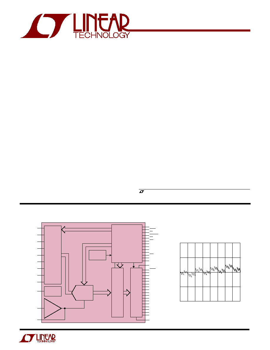
BLOCK DIAGRA
W
APPLICATIO S
U
FEATURES
DESCRIPTIO
U
8-Channel, 10-Bit/12-Bit,
400ksps, Low Power, Sampling ADCs
The 10-bit LTC
®
1852 and 12-bit LTC1853 are complete
8-channel data acquisition systems. They include a flex-
ible 8-channel multiplexer, a 400ksps successive approxi-
mation analog-to-digital converter, an internal reference
and a parallel output interface. The multiplexer can be
configured for single-ended or differential inputs, two gain
ranges and unipolar or bipolar operation. The ADCs have
a scan mode that will repeatedly cycle through all 8
multiplexer channels and can also be programmed to
sequence through up to 16 addresses and configurations.
The sequence can also be read back from internal memory.
The reference and buffer amplifier provide pin strappable
ranges of 4.096V, 2.5V and 2.048V. The parallel output
includes the 10-bit or 12-bit conversion result plus the 4-
bit multiplexer address. The digital outputs are powered
from a separate supply allowing for easy interface to 3V
digital logic. Typical power consumption is 10mW at
400ksps from a single 5V supply and 3mW at 250ksps
from a single 3V supply.
s
Flexible 8-Channel Multiplexer
Single-Ended or Differential Inputs
Two Gain Ranges
Unipolar or Bipolar Operation
s
Scan Mode and Programmable Sequencer
Eliminate Configuration Software Overhead
s
Low Power: 3mW at 250ksps
s
2.7V to 5.5V Supply Range
s
Internal or External Reference Operation
s
Parallel Output Includes MUX Address
s
Nap and Sleep Shutdown Modes
s
Pin Compatible up-grade 1.25Msps 10-Bit LTC1850
and 12-Bit LTC1851
s
High Speed Data Acquisition
s
Test and Measurement
s
Imaging Systems
s
Telecommunications
s
Industrial Process Control
s
Spectrum Analysis
BUSY
DIFF
OUT
/S6
A2
OUT
/S5
A1
OUT
/S4
A0
OUT
/S3
D11/S2
D10/S1
D9/S0
D8
D7
D6
D5
D4
D3
D2
D1
D0
M1
SHDN
CS
CONVST
RD
WR
DIFF
A2
A1
A0
UNI/BIP
PGA
M0
OUTPUT
DRIVERS
DATA
LATCHES
OGND
18523 BD
OV
DD
REF AMP
REFCOMP
REFIN
REFOUT
COM
CH7
CH6
CH5
CH4
CH3
CH2
CH1
CH0
8-CHANNEL
MULTIPLEXER
2.5V
REFERENCE
INTERNAL
CLOCK
LTC1853
CONTROL LOGIC
AND
PROGRAMMABLE
SEQUENCER
12-BIT
SAMPLING
ADC
+
, LTC and LT are registered trademarks of Linear Technology Corporation.
Integral Linearity
0
512 1024 1536 2048 2560 3072 3584 4096
CODE
1.0
0.5
0
0.5
1.0
INL ERROR (LSBs)
1852 F01
2
LTC1852/LTC1853
18523f
A
U
G
W
A
W
U
W
A
R
BSOLUTE
XI
TI
S
OV
DD
= V
DD
(Notes 1, 2)
Supply Voltage (V
DD
) ................................................. 6V
Analog Input Voltage (Note 3) ..... 0.3V to (V
DD
+ 0.3V)
Digital Input Voltage (Note 4) .................... 0.3V to 10V
Digital Output Voltage .................. 0.3V to (V
DD
+ 0.3V)
Power Dissipation .............................................. 500mW
W
U
U
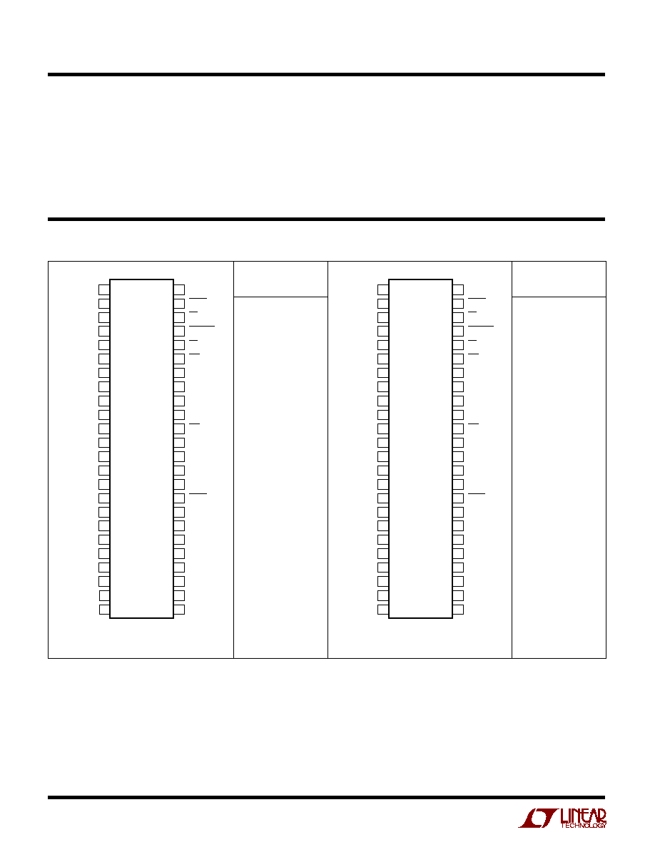
PACKAGE/ORDER I FOR ATIO
ORDER PART
NUMBER
LTC1853CFW
LTC1853IFW
T
JMAX
= 150
°
C,
JA
= 110
°
C/W
1
2
3
4
5
6
7
8
9
10
11
12
13
14
15
16
17
18
19
20
21
22
23
24
TOP VIEW
FW PACKAGE
48-LEAD PLASTIC TSSOP
48
47
46
45
44
43
42
41
40
39
38
37
36
35
34
33
32
31
30
29
28
27
26
25
CH0
CH1
CH2
CH3
CH4
CH5
CH6
CH7
COM
REFOUT
REFIN
REFCOMP
GND
V
DD
V
DD
GND
DIFF
OUT
/S6
A2
OUT
/S5
A1
OUT
/S4
A0
OUT
/S3
D11/S2
D10/S1
D9/S0
D8
M1
SHDN
CS
CONVST
RD
WR
DIFF
A2
A1
A0
UNI/BIP
PGA
M0
OV
DD
OGND
BUSY
D0
D1
D2
D3
D4
D5
D6
D7
Consult LTC Marketing for parts specified with wider operating temperature ranges.
ORDER PART
NUMBER
LTC1852CFW
LTC1852IFW
T
JMAX
= 150
°
C,
JA
= 110
°
C/W
1
2
3
4
5
6
7
8
9
10
11
12
13
14
15
16
17
18
19
20
21
22
23
24
TOP VIEW
FW PACKAGE
48-LEAD PLASTIC TSSOP
48
47
46
45
44
43
42
41
40
39
38
37
36
35
34
33
32
31
30
29
28
27
26
25
CH0
CH1
CH2
CH3
CH4
CH5
CH6
CH7
COM
REFOUT
REFIN
REFCOMP
GND
V
DD
V
DD
GND
DIFF
OUT
/S6
A2
OUT
/S5
A1
OUT
/S4
A0
OUT
/S3
D9/S2
D8/S1
D7/S0
D6
M1
SHDN
CS
CONVST
RD
WR
DIFF
A2
A1
A0
UNI/BIP
PGA
M0
OV
DD
OGND
BUSY
NC
NC
D0
D1
D2
D3
D4
D5
Ambient Operating Temperature Range
LTC1852C/LTC1853C ............................ 0
°
C to 70
°
C
LTC1852I/LTC1853I .......................... 40
°
C to 85
°
C
Storage Temperature Range ................. 65
°
C to 150
°
C
Lead Temperature (Soldering, 10 sec)................ 300
°
C
3
LTC1852/LTC1853
18523f
SYMBOL
PARAMETER
CONDITIONS
MIN
TYP
MAX
UNITS
V
IN
Analog Input Range (Note 9)
2.7V
V
DD
5.5V, REFCOMP
V
DD
Unipolar, Gain = 1 (PGA = 1)
0 REFCOMP
V
Unipolar, Gain = 2 (PGA = 0)
0 REFCOMP/2
V
Bipolar, Gain = 1 (PGA = 1)
±
REFCOMP/2
V
Bipolar, Gain = 2 (PGA = 0)
±
REFCOMP/4
V
I
IN
Analog Input Leakage Current
q
±
1
µ
A
C
IN
Analog Input Capacitance
Between Conversions (Gain = 1)
15
pF
Between Conversions (Gain = 2)
25
pF
During Conversions
5
pF
t
ACQ
Sample-and-Hold Acquisition Time
50
150
ns
t
S(MUX)
Multiplexer Settling Time (Includes t
ACQ
)
50
150
ns
t
AP
Sample-and-Hold Aperture Delay Time
V
DD
= 5V
0.5
ns
t
jitter
Sample-and-Hold Aperture Delay Time Jitter
V
DD
= 5V
2
ps
RMS
CMRR
Analog Input Common Mode Rejection Ratio
60
dB
LTC1852
LTC1853
PARAMETER
CONDITIONS
MIN
TYP
MAX
MIN
TYP
MAX
UNITS
Resolution (No Missing Codes)
q
10
12
Bits
Integral Linearity Error
(Note 7)
q
±
0.25
±
1
±
0.35
±
1
LSB
Differential Linearity Error
q
±
0.25
±
1
±
0.25
±
1
LSB
Offset Error (Bipolar and Unipolar)
(Note 8)
Gain = 1 (PGA = 1)
REFCOMP
2V
q
±
0.5
±
2
±
1
±
6
LSB
Gain = 2 (PGA = 0)
q
±
1
±
4
±
2
±
12
LSB
Offset Error Match (Bipolar and Unipolar)
±
0.5
±
1
LSB
Unipolar Gain Error
With External 4.096V Reference
Gain = 1 (PGA = 1)
Applied to REFCOMP (Note 12)
±
2
±
4
LSB
Gain = 2 (PGA = 0)
V
DD
= 4.75V to 5.25V, f
S
400kHz
±
4
±
8
LSB
Unipolar Gain Error Match
±
0.5
±
1
LSB
Bipolar Gain Error
With External 4.096V Reference
Gain = 1 (PGA = 1)
Applied to REFCOMP (Note 12)
±
2
±
4
LSB
Gain = 2 (PGA = 0)
V
DD
= 4.75V to 5.25V, f
S
400kHz
±
4
±
8
LSB
Bipolar Gain Error Match
±
0.5
±
1
LSB
Unipolar Gain Error
With External 2.5V Reference
Gain = 1 (PGA = 1)
Applied to REFCOMP
q
±
1
±
3
±
1.5
±
8
LSB
Gain = 2 (PGA = 0)
V
DD
= 2.7V to 5.5V, f
S
250kHz
q
±
2
±
6
±
3
±
16
LSB
Bipolar Gain Error
With External 2.5V Reference
Gain = 1 (PGA = 1)
Applied to REFCOMP
q
±
1
±
3
±
1.5
±
8
LSB
Gain = 2 (PGA = 0)
V
DD
= 2.7V to 5.5V, f
S
250kHz
q
±
2
±
6
±
3
±
16
LSB
Full-Scale Error Temperature Coefficient
15
15
ppm/
°
C
The
q
denotes the specifications which apply over the full operating temperature range, otherwise
specifications are at T
A
= 25
°
C. (Note 5)
A ALOG I PUT
U
U
The
q
denotes the specifications which apply over the full operating
temperature range, otherwise specifications are at T
A
= 25
°
C. V
DD
= 2.7V to 5.5V, REFCOMP < V
DD
(Notes 5, 6)
CO VERTER CHARACTERISTICS
U
SYMBOL
PARAMETER
CONDITIONS
MIN
TYP
MAX
UNITS
S/(N + D)
Signal-to-Noise Plus Distortion Ratio
40kHz Input Signal
72.5
dB
THD
Total Harmonic Distortion
40kHz Input Signal, First 5 Harmonics
80
dB
SFDR
Spurious Free Dynamic Range
40kHz Input Signal
85
dB
DY
A
IC ACCURACY
U
W
T
A
= 25
°
C. (Note 5)
4
LTC1852/LTC1853
18523f
PARAMETER
CONDITIONS
MIN
TYP
MAX
UNITS
REFOUT Output Voltage
I
OUT
= 0
2.48
2.50
2.52
V
REFOUT Output Temperature Coefficient I
OUT
= 0
±
15
ppm/
°
C
REFOUT Line Regulation
2.7
V
DD
5.5, I
OUT
= 0
0.01
LSB/V
Reference Buffer Gain
1.6368
1.6384
1.6400
V/V
REFCOMP Output Voltage
External 2.5V Reference (V
DD
= 5V)
4.092
4.096
4.100
V
Internal 2.5V Reference (V
DD
= 5V)
4.060
4.096
4.132
V
REFCOMP Impedance
Impedance to GND, REFIN = V
DD
19.2
k
T
A
= 25
°
C. (Notes 5, 6)
I TER AL REFERE CE
U
U
U
The
q
denotes the specifications which apply over the
full operating temperature range, otherwise specifications are at T
A
= 25
°
C. V
DD
= 5V (Note 5)
DIGITAL I PUTS A D DIGITAL OUTPUTS
U
U
SYMBOL
PARAMETER
CONDITIONS
MIN
TYP
MAX
UNITS
V
IH
High Level Input Voltage
V
DD
= 3.3V
q
1.9
V
V
IL
Low Level Input Voltage
V
DD
= 2.7V
q
0.45
V
I
IN
Digital Input Current
V
IN
= 0V to V
DD
q
±
5
µ
A
C
IN
Digital Input Capacitance
1.5
pF
V
OH
High Level Output Voltage
V
DD
= 2.7V, I
O
= 10
µ
A
2.5
V
V
DD
= 2.7V, I
O
= 200
µ
A
q
2
V
V
OL
Low Level Output Voltage
V
DD
= 2.7V, I
O
= 160
µ
A
0.05
V
V
DD
= 2.7V, I
O
= 1.6mA
q
0.10
0.4
V
I
OZ
Hi-Z Output Leakage D11 to D0, A0, A1, A2
OUT
, DIFF
OUT
V
OUT
= 0V to V
DD
, CS High
q
±
10
µ
A
C
OZ
Hi-Z Capacitance D11 to D0
CS High (Note 9)
q
15
pF
I
SOURCE
Output Source Current
V
OUT
= 0V
10
mA
I
SINK
Output Sink Current
V
OUT
= V
DD
15
mA
The
q
denotes the specifications which apply over the
full operating temperature range, otherwise specifications are at T
A
= 25
°
C. V
DD
= 3V (Note 5)
DIGITAL I PUTS A D DIGITAL OUTPUTS
U
U
SYMBOL
PARAMETER
CONDITIONS
MIN
TYP
MAX
UNITS
V
IH
High Level Input Voltage
V
DD
= 5.25V
q
2.4
V
V
IL
Low Level Input Voltage
V
DD
= 4.75V
q
0.8
V
I
IN
Digital Input Current
V
IN
= 0V to V
DD
q
±
5
µ
A
C
IN
Digital Input Capacitance
1.5
pF
V
OH
High Level Output Voltage
V
DD
= 4.75V, I
O
= 10
µ
A
4.5
V
V
DD
= 4.75V, I
O
= 200
µ
A
q
4
V
V
OL
Low Level Output Voltage
V
DD
= 4.75V, I
O
= 160
µ
A
0.05
V
V
DD
= 4.75V, I
O
= 1.6mA
q
0.10
0.4
V
I
OZ
Hi-Z Output Leakage D11 to D0, A0, A1, A2
OUT
, DIFF
OUT
V
OUT
= 0V to V
DD
, CS High
q
±
10
µ
A
C
OZ
Hi-Z Capacitance D11 to D0
CS High (Note 9)
q
15
pF
I
SOURCE
Output Source Current
V
OUT
= 0V
20
mA
I
SINK
Output Sink Current
V
OUT
= V
DD
30
mA

5
LTC1852/LTC1853
18523f
SYMBOL
PARAMETER
CONDITIONS
MIN
TYP
MAX
UNITS
f
SAMPLE(MAX)
Maximum Sampling Frequency
V
DD
= 5.5V
q
400
kHz
V
DD
= 2.7V
q
250
kHz
Acquisition + Conversion
V
DD
= 5.5V
q
2.5
µ
s
V
DD
= 2.7V
q
4.0
µ
s
t
CONV
Conversion Time
V
DD
= 5.5V
q
2.0
µ
s
V
DD
= 2.7V
q
3.5
µ
s
t
ACQ
Acquisition Time
(Note 13)
q
150
ns
t
1
CS to RD Setup Time
(Notes 9, 10)
q
0
ns
t
2
CS to CONVST Setup Time
(Notes 9, 10)
q
10
ns
t
3
CS to SHDN Setup Time
(Notes 9, 10)
200
ns
t
4
SHDN to CONVST Wake-Up Time
Nap Mode (Note 10)
200
ns
Sleep Mode (Note 10)
10
ms
t
5
CONVST Low Time
(Notes 10, 11)
q
50
ns
t
6
CONVST to BUSY Delay
C
L
= 25pF
10
ns
q
60
ns
t
7
Data Ready Before BUSY
20
35
ns
q
15
ns
t
8
Delay Between Conversions
(Note 10)
q
50
ns
t
9
Wait Time RD After BUSY
q
5
ns
t
10
Data Access Time After RD
C
L
= 25pF
20
35
ns
q
45
ns
C
L
= 100pF
25
45
ns
q
60
ns
t
11
BUS Relinquish Time
10
30
ns
0
°
C to 70
°
C
q
35
ns
40
°
C to 85
°
C
q
40
ns
SYMBOL
PARAMETER
CONDITIONS
MIN
TYP
MAX
UNITS
V
DD
Analog Positive Supply Voltage
(Note 10)
q
2.7
5.5
V
OV
DD
Output Positive Supply Voltage
(Note 10)
q
2.7
5.5
V
I
DD
Positive Supply Current
V
DD
= OV
DD
= 5V, f
S
= 400kHz
q
2
3
mA
V
DD
= OV
DD
= 2.7V, f
S
= 250kHz
q
0.83
1.33
mA
P
DISS
Power Dissipation
V
DD
= OV
DD
= 5V, f
S
= 400kHz
q
10
15
mW
V
DD
= OV
DD
= 2.7V, f
S
= 250kHz
q
2.25
4
mW
I
DDPD
Power Down Positive Supply Current
Nap Mode
SHDN = Low, CS = Low
0.5
mA
Sleep Mode
SHDN = Low, CS = High
20
µ
A
Power Down Power Dissipation
V
DD
= V
DD
= OV
DD
= 5V, f
S
= 400kHz
Nap Mode
SHDN = Low, CS = Low
2.5
mW
Sleep Mode
SHDN = Low, CS = High
0.1
mW
Power Down Power Dissipation
V
DD
= V
DD
= OV
DD
= 3V, f
S
= 250kHz
Nap Mode
SHDN = Low, CS = Low
1.5
mW
Sleep Mode
SHDN = Low, CS = High
0.06
mW
The
q
denotes the specifications which apply over the full operating temperature
range, otherwise specifications are at T
A
= 25
°
C. (Note 5)
POWER REQUIRE E TS
W
U
The
q
denotes the specifications which apply over the full operating temperature
range, otherwise specifications are at T
A
= 25
°
C. (Note 5)
TI I G CHARACTERISTICS
U
W