
1
LTC1871
Wide Input Range, No R
SENSE
TM
Current Mode Boost, Flyback and SEPIC Controller
The LTC
Æ
1871 is a wide input range, current mode, boost,
flyback and SEPIC controller that drives an N-channel
power MOSFET and requires very few external compo-
nents. Intended for low to medium power applications, it
eliminates the need for a current sense resistor by utiliz-
ing the power MOSFET's on-resistance, thereby maximiz-
ing efficiency.
The IC's operating frequency can be set with an external
resistor over a 50kHz to 1MHz range, and can be synchro-
nized to an external clock using the MODE/SYNC pin.
Burst Mode operation at light loads, a low minimum
operating supply voltage of 2.5V and a low shutdown
quiescent current of 10
µ
A make the LTC1871 ideally
suited for battery-operated systems.
For applications requiring constant frequency operation,
Burst Mode operation can be defeated using the MODE/
SYNC pin. Higher output voltage boost, SEPIC and fly-
back applications are possible with the LTC1871 by
connecting the SENSE pin to a resistor in the source of the
power MOSFET.
The LTC1871 is available in the 10-lead MSOP package.
s
High Efficiency (No Sense Resistor Required)
s
Wide Input Voltage Range: 2.5V to 36V
s
Current Mode Control Provides Excellent
Transient Response
s
High Maximum Duty Cycle (92% Typ)
s
±
2% RUN Pin Threshold with 100mV Hysteresis
s
±
1% Internal Voltage Reference
s
Micropower Shutdown: I
Q
= 10
µ
A
s
Programmable Operating Frequency
(50kHz to 1MHz) with One External Resistor
s
Synchronizable to an External Clock Up to 1.3
◊
f
OSC
s
User-Controlled Pulse Skip or Burst Mode
Æ
Operation
s
Internal 5.2V Low Dropout Voltage Regulator
s
Output Overvoltage Protection
s
Capable of Operating with a Sense Resistor for High
Output Voltage Applications
s
Small 10-Lead MSOP Package
s
Telecom Power Supplies
s
Portable Electronic Equipment
Burst Mode is a registered trademark of Linear Technology Corporation.
No R
SENSE
is a trademark of Linear Technology Corporation.
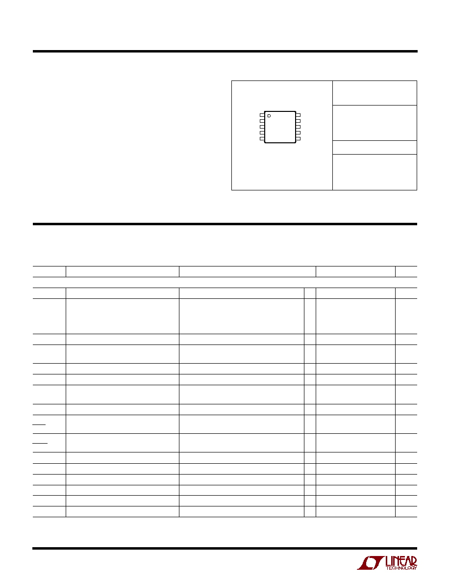
Figure 1. High Efficiency 3.3V Input, 5V Output Boost Converter (Bootstrapped)
Efficiency of Figure 1
, LTC and LT are registered trademarks of Linear Technology Corporation.
OUTPUT CURRENT (A)
30
EFFICIENCY (%)
90
100
80
50
70
60
40
0.001
0.1
1
10
1871 F01b
0.01
Burst Mode
OPERATION
PULSE-SKIP
MODE
DESCRIPTIO
U
FEATURES
APPLICATIO S
U
TYPICAL APPLICATIO
U
+
RUN
I
TH
FB
FREQ
MODE/SYNC
SENSE
V
IN
INTV
CC
GATE
GND
LTC1871
R
T
80.6k
1%
R2
37.4k
1%
R1
12.1k
1%
C
VCC
4.7
µ
F
X5R
C
IN
22
µ
F
6.3V
◊
2
M1
D1
L1
1
µ
H
R
C
22k
C
C1
6.8nF
C
C2
47pF
C
OUT1
150
µ
F
6.3V
◊
4
V
IN
3.3V
V
OUT
5V
7A
(10A PEAK)
GND
1871 F01a
+
C
OUT2
22
µ
F
6.3V
X5R
◊
2
C
IN
:
TAIYO YUDEN JMK325BJ226MM
C
OUT1
: PANASONIC EEFUEOJ151R
C
OUT2
: TAIYO YUDEN JMK325BJ226MM
D1: MBRB2515L
L1: SUMIDA CEP125-H 1R0MH
M1: FAIRCHILD FDS7760A
2
LTC1871
(Note 1)
V
IN
Voltage ............................................... ≠ 0.3V to 36V
INTV
CC
Voltage ........................................... ≠ 0.3V to 7V
INTV
CC
Output Current ........................................ 50mA
GATE Voltage ........................... ≠ 0.3V to V
INTVCC
+ 0.3V
I
TH
, FB Voltages ....................................... ≠ 0.3V to 2.7V
RUN, MODE/SYNC Voltages ....................... ≠ 0.3V to 7V
FREQ Voltage ............................................≠ 0.3V to 1.5V
SENSE Pin Voltage ................................... ≠ 0.3V to 36V
Operating Temperature Range (Note 2) .. ≠ 40
∞
C to 85
∞
C
Junction Temperature (Note 3) ............................ 125
∞
C
Storage Temperature Range ................. ≠ 65
∞
C to 150
∞
C
Lead Temperature (Soldering, 10 sec).................. 300
∞
C
ORDER PART
NUMBER
LTC1871EMS
T
JMAX
= 125
∞
C,
JA
= 120
∞
C/ W
ABSOLUTE AXI U RATI GS
W
W
W
U
PACKAGE/ORDER I FOR ATIO
U
U
W
ELECTRICAL CHARACTERISTICS
MS PART MARKING
LTSX
1
2
3
4
5
RUN
I
TH
FB
FREQ
MODE/
SYNC
10
9
8
7
6
SENSE
V
IN
INTV
CC
GATE
GND
TOP VIEW
MS PACKAGE
10-LEAD PLASTIC MSOP
SYMBOL
PARAMETER
CONDITIONS
MIN
TYP
MAX
UNITS
Main Control Loop
V
IN(MIN)
Minimum Input Voltage
2.5
V
I
Q
Input Voltage Supply Current
(Note 4)
Continuous Mode
V
MODE/SYNC
= 5V, V
FB
= 1.4V, V
ITH
= 0.75V
550
1000
µ
A
Burst Mode Operation, No Load
V
MODE/SYNC
= 0V, V
ITH
= 0.2V (Note 5)
250
500
µ
A
Shutdown Mode
V
RUN
= 0V
10
20
µ
A
V
RUN
+
Rising RUN Input Threshold Voltage
1.348
V
V
RUN
≠
Falling RUN Input Threshold Voltage
1.223
1.248
1.273
V
q
1.198
1.298
V
V
RUN(HYST)
RUN Pin Input Threshold Hysteresis
50
100
150
mV
I
RUN
RUN Input Current
1
60
nA
V
FB
Feedback Voltage
V
ITH
= 0.2V (Note 5)
1.218
1.230
1.242
V
q
1.212
1.248
V
I
FB
FB Pin Input Current
V
ITH
= 0.2V (Note 5)
18
60
nA
V
FB
Line Regulation
2.5V
V
IN
30V
0.002
0.02
%/V
V
IN
V
FB
Load Regulation
V
MODE/SYNC
= 0V, V
TH
= 0.5V to 0.90V (Note 5)
q
≠ 1
≠ 0.1
%
V
ITH
V
FB(OV)
FB Pin, Overvoltage Lockout
V
FB(OV)
≠ V
FB(NOM)
in Percent
2.5
6
10
%
g
m
Error Amplifier Transconductance
I
TH
Pin Load =
±
5
µ
A (Note 5)
650
µ
mho
V
ITH(BURST)
Burst Mode Operation I
TH
Pin Voltage
Falling I
TH
Voltage (Note 5)
0.3
V
V
SENSE(MAX)
Maximum Current Sense Input Threshold
Duty Cycle < 20%
120
150
180
mV
I
SENSE(ON)
SENSE Pin Current (GATE High)
V
SENSE
= 0V
35
50
µ
A
I
SENSE(OFF)
SENSE Pin Current (GATE Low)
V
SENSE
= 30V
0.1
5
µ
A
The
q
denotes specifications which apply over the full operating temperature range, otherwise specifications are at T
A
= 25
∞
C.
V
IN
= V
INTVCC
= 5V, V
RUN
= 1.5V, R
FREQ
= 80k, V
MODE/SYNC
= 0V, unless otherwise specified.
Consult LTC Marketing for parts specified with wider operating temperature ranges.

3
LTC1871
ELECTRICAL CHARACTERISTICS
Note 1: Absolute Maximum Ratings are those values beyond which the life
of the device may be impaired.
Note 2: The LTC1871E is guaranteed to meet performance specifications
from 0
∞
C to 70
∞
C. Specifications over the ≠ 40
∞
C to 85
∞
C operating
temperature range are assured by design, characterization and correlation
with statistical process controls.
Note 3: T
J
is calculated from the ambient temperature T
A
and power
dissipation P
D
according to the following formula:
T
J
= T
A
+ (P
D
∑ 120
∞
C/W)
Note 4: The dynamic input supply current is higher due to power MOSFET
gate charging (Q
G
∑ f
OSC
). See Applications Information.
Note 5: The LTC1871 is tested in a feedback loop that servos V
FB
to the
reference voltage with the I
TH
pin forced to a voltage between 0V and 1.4V
(the no load to full load operating voltage range for the I
TH
pin is 0.3V to
1.23V).
Note 6: In a synchronized application, the internal slope compensation
gain is increased by 25%. Synchronizing to a significantly higher ratio will
reduce the effective amount of slope compensation, which could result in
subharmonic oscillation for duty cycles greater than 50%.
Note 7: Rise and fall times are measured at 10% and 90% levels.
The
q
denotes specifications which apply over the full operating temperature range, otherwise specifications are at T
A
= 25
∞
C.
V
IN
= V
INTVCC
= 5V, V
RUN
= 1.5V, R
FREQ
= 80k, V
MODE/SYNC
= 0V, unless otherwise specified.
SYMBOL
PARAMETER
CONDITIONS
MIN
TYP
MAX
UNITS
Oscillator
f
OSC
Oscillator Frequency
R
FREQ
= 80k
250
300
350
kHz
Oscillator Frequency Range
50
1000
kHz
D
MAX
Maximum Duty Cycle
87
92
97
%
f
SYNC/
f
OSC
Recommended Maximum Synchronized
f
OSC
= 300kHz (Note 6)
1.25
1.30
Frequency Ratio
t
SYNC(MIN)
MODE/SYNC Minimum Input Pulse Width
V
SYNC
= 0V to 5V
25
ns
t
SYNC(MAX)
MODE/SYNC Maximum Input Pulse Width
V
SYNC
= 0V to 5V
0.8/f
OSC
ns
V
IL(MODE)
Low Level MODE/SYNC Input Voltage
0.3
V
V
IH(MODE)
High Level MODE/SYNC Input Voltage
1.2
V
R
MODE/SYNC
MODE/SYNC Input Pull-Down Resistance
50
k
V
FREQ
Nominal FREQ Pin Voltage
0.62
V
Low Dropout Regulator
V
INTVCC
INTV
CC
Regulator Output Voltage
V
IN
= 7.5V
5.0
5.2
5.4
V
V
INTVCC
INTV
CC
Regulator Line Regulation
7.5V
V
IN
15V
8
25
mV
V
IN1
V
INTVCC
INTV
CC
Regulator Line Regulation
15V
V
IN
30V
70
200
mV
V
IN2
V
LDO(LOAD)
INTV
CC
Load Regulation
0
I
INTVCC
20mA, V
IN
= 7.5V
≠ 2
≠ 0.2
%
V
DROPOUT
INTV
CC
Regulator Dropout Voltage
V
IN
= 5V, INTV
CC
Load = 20mA
280
mV
I
INTVCC
Bootstrap Mode INTV
CC
Supply
RUN = 0V, SENSE = 5V
10
20
µ
A
Current in Shutdown
GATE Driver
t
r
GATE Driver Output Rise Time
C
L
= 3300pF (Note 7)
17
100
ns
t
f
GATE Driver Output Fall Time
C
L
= 3300pF (Note 7)
8
100
ns

4
LTC1871
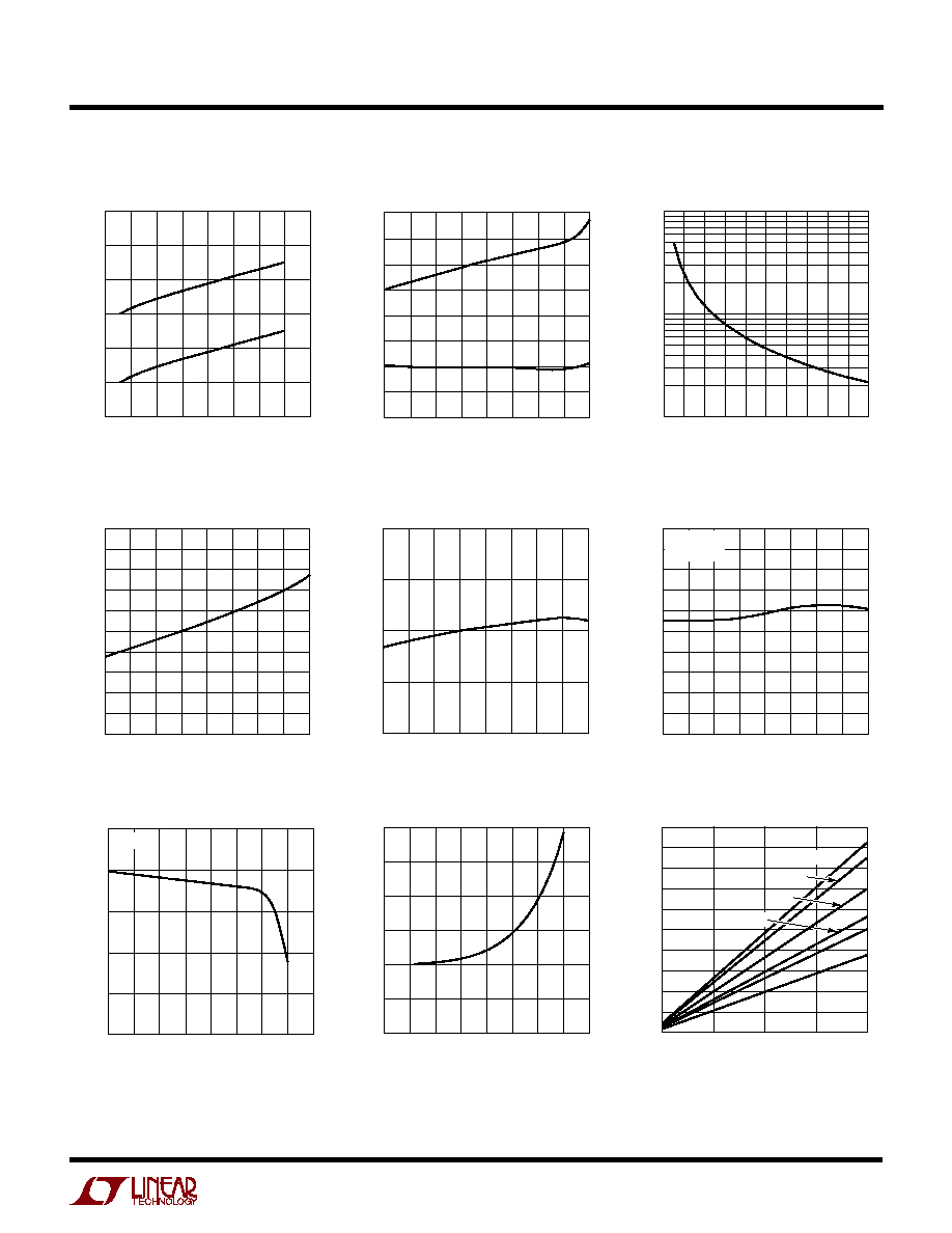
TYPICAL PERFOR A CE CHARACTERISTICS
U
W
FB Voltage vs Temp
FB Voltage Line Regulation
FB Pin Current vs Temperature
TEMPERATURE (
∞
C)
≠50
FB VOLTAGE (V)
1.23
1.24
150
1871 G01
1.22
1.21
0
50
100
≠25
25
75
125
1.25
V
IN
(V)
0
1.229
FB VOLTAGE (V)
1.230
1.231
5
10
15
20
1871 G02
25
30
35
TEMPERATURE (
∞
C)
≠50
0
FB PIN CURRENT (nA)
10
20
30
40
60
≠25
25
0
50
100
75
1871 G03
125 150
50
Shutdown Mode I
Q
vs V
IN
Burst Mode I
Q
vs V
IN
V
IN
(V)
0
0
SHUTDOWN MODE I
Q
(
µ
A)
10
20
10
20
30
40
1871 G04
30
Shutdown Mode I
Q
vs Temperature
TEMPERATURE (
∞
C)
≠50
0
SHUTDOWN MODE I
Q
(
µ
A)
5
10
15
20
≠25
0
25
50
1871 G05
75
100 125 150
V
IN
= 5V
V
IN
(V)
0
0
Burst Mode I
Q
(
µ
A)
100
200
300
400
600
10
20
1871 G06
30
40
500
Burst Mode I
Q
vs Temperature
Gate Drive Rise and Fall Time
vs C
L
Dynamic I
Q
vs Frequency
TEMPERATURE (
∞
C)
≠50
0
Burst Mode I
Q
(
µ
A)
200
500
0
50
75
1871 G07
100
400
300
≠25
25
100 125
150
FREQUENCY (kHz)
0
0
I
Q
(mA)
2
6
8
10
800
18
1871 G08
4
400
1200
600
200
1000
12
14
16
C
L
= 3300pF
I
Q(TOT)
= 550
µ
A + Qg ∑ f
C
L
(pF)
0
0
TIME (ns)
10
20
30
40
60
2000
4000
6000
8000
1871 G09
10000 12000
50
RISE TIME
FALL TIME
5
LTC1871
TYPICAL PERFOR A CE CHARACTERISTICS
U
W
RUN Thresholds vs V
IN
R
T
vs Frequency
Frequency vs Temperature
SENSE Pin Current vs Temperature
Maximum Sense Threshold
vs Temperature
INTV
CC
Load Regulation
INTV
CC
Dropout Voltage
vs Current, Temperature
INTV
CC
Line Regulation
V
IN
(V)
0
1.2
RUN THRESHOLDS (V)
1.3
1.4
10
20
30
40
1871 G10
1.5
RUN Thresholds vs Temperature
TEMPERATURE (
∞
C)
≠50
RUN THRESHOLDS (V)
1.30
1.35
150
1871 G11
1.25
1.20
0
50
100
≠25
25
75
125
1.40
FREQUENCY (kHz)
100
R
T
(k
)
300
1000
1871 G12
10
100
200
1000
900
800
700
600
500
400
0
TEMPERATURE (
∞
C)
≠50
275
GATE FREQUENCY (kHz)
280
290
295
300
325
310
0
50
75
1871 G13
285
315
320
305
≠25
25
100 125
150
TEMPERATURE (
∞
C)
≠50
140
MAX SENSE THRESHOLD (mV)
145
150
155
160
≠25
0
25
50
1871 G14
75
100 125 150
TEMPERATURE (
∞
C)
≠50
25
SENSE PIN CURRENT (
µ
A)
30
35
0
50
75
1871 G15
≠25
25
100 125
150
GATE HIGH
V
SENSE
= 0V
INTV
CC
LOAD (mA)
0
INTV
CC
VOLTAGE (V)
5.2
30
50
80
1871 G16
5.1
5.0
10
20
40
60
70
V
IN
= 7.5V
V
IN
(V)
0
5.1
INTV
CC
VOLTAGE (V)
5.2
5.3
10
20
30
40
1871 G17
5.4
5
15
25
35
INTV
CC
LOAD (mA)
0
0
DROPOUT VOLTAGE (mV)
50
150
200
250
500
350
5
10
1871 G18
100
400
450
300
15
20
150
∞
C
75
∞
C
125
∞
C
25
∞
C
≠50
∞
C
0
∞
C