 | –≠–ª–µ–∫—Ç—Ä–æ–Ω–Ω—ã–π –∫–æ–º–ø–æ–Ω–µ–Ω—Ç: LTC1876EG | –°–∫–∞—á–∞—Ç—å:  PDF PDF  ZIP ZIP |
LTC1876
1
1876fa
APPLICATIO S
U
FEATURES
DESCRIPTIO
U
TYPICAL APPLICATIO
U
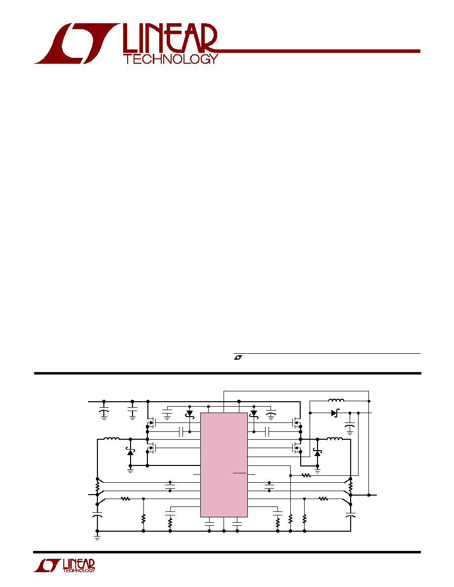
High Efficiency, 2-Phase,
Dual Synchronous Step-Down Switching
Controller and Step-Up Regulator
The LTC
Æ
1876 is a high performance triple output switching
regulator. It incorporates a dual step-down switching con-
troller that drives all N-channel synchronous power MOSFET
stages. A step-up regulator with an internal 1A, 36V switch
provides the third output.
The step-down controllers minimize power loss and noise
by operating the output stage of each controller out of
phase. OPTI-LOOP compensation allows the transient
response to be optimized over a wide range of output
capacitance and ESR values. A RUN/SS pin for each
controller provides both soft-start and an optional timed,
short-circuit shutdown that can be configured to latch off
one or both controllers. Current foldback provides
additional short-circuit protection. In an overvoltage
condition, the bottom MOSFET is latched on until V
OUT
returns to normal. The FCB pin can be used to inhibit Burst
Mode operation or to enable regulation of a secondary
output voltage.
The step-up regulator operates at 1.2MHz, allowing the
use of tiny low cost capacitors and inductors. In addition,
its internal 1A switch allows high current outputs to be
generated. Its current mode control scheme provides
excellent line and load regulation.
Step-Down Controller
s
Out-of-Phase Controllers Reduce Required Input
Capacitance and Power Supply Induced Noise
s
Power Good Output Voltage Indicator
s
OPTI-LOOP
TM
Compensation Minimizes C
OUT
s
DC Programmed Fixed Frequency 150kHz to 300kHz
s
Wide V
IN
Range: 3.5V to 36V Operation
s
Very Low Dropout Operation: 99% Duty Cycle
s
Adjustable Soft-Start Current Ramping
s
Latched Short-Circuit Shutdown with Defeat Option
s
Remote Output Voltage Sense and OV Protection
s
5V and 3.3V Standby Regulators
s
Selectable Const. Freq. or Burst Mode
TM
Operation
Step-Up Regulator
s
High Operating Switching Frequency of 1.2MHz
s
Low Internal V
CESAT
Switch: 400mV @ 1A, V
IN
= 3V
s
Wide V
IN
Range: 2.6V to 16V Operation
s
High Output Voltage: Up to 34V
s
3.3V Input Step-Down Converter
s
Notebook and Palmtop Computers, PDAs
s
Battery-Operated Digital Devices
, LTC and LT are registered trademarks of Linear Technology Corporation.
Burst Mode and OPTI-LOOP are trademarks of Linear Technology Corporation.
Figure 1. High Efficiency Triple 5V/3.3V/12V Power Supply
4.7
µ
F
10V
M4
M3
0.1
µ
F
63.4k
1%
1000pF
6.3
µ
H
220pF
1
µ
F
CER
33
µ
F
35V
ALUM
10
µ
F
35V
CER
+
56
µ
F
4V
SP
0.01
20k
1%
15k
V
OUT2
3.3V
5A
M2
M1
0.1
µ
F
105k
1%
6.8
µ
H
220pF
1000pF
+
+
+
+
47
µ
F
6.3V
SP
0.01
20k
1%
10.2k
1%
15k
V
OUT1
5V
4A
V
OUT3
12V
200mA
TG2
TG1
BOOST2
BOOST1
SW2
SW1
BG2
BG1
PGND
PGOOD
AUXSW
AUXV
FB
AUXSD
SENSE2
+
SENSE1
+
SENSE2
≠
SENSE1
≠
V
OSENSE2
V
OSENSE1
I
TH2
I
TH1
AUXV
IN
V
IN
INTV
CC
RUN/SS2
RUN/SS1
V
IN
5.2V
TO 28V
M1, M2, M3, M4: FDS6680A
1876 TA01
0.1
µ
F
0.1
µ
F
LTC1876
SGND
86.6k, 1%
10
µ
H
10
µ
F
20V
LTC1876
2
1876fa
SYMBOL
PARAMETER
CONDITIONS
MIN
TYP
MAX
UNITS
Main Control Loops
V
OSENSE1, 2
Regulated Feedback Voltage
I
TH1, 2
Voltage = 1.2V (Note 4)
q
0.792
0.800
0.808
V
I
VOSENSE1, 2
Feedback Current
(Note 4)
≠5
≠50
nA
V
REFLNREG
Reference Voltage Line Regulation
V
IN
= 3.6V to 30V (Note 4)
0.002
0.02
%/V
V
LOADREG
Output Voltage Load Regulation
(Note 4)
Measured in Servo Loop;
I
TH
Voltage = 1.2V to 0.7V
q
0.1
0.5
%
Measured in Servo Loop;
I
TH
Voltage = 1.2V to 2V
q
≠0.1
≠0.5
%
g
m1, 2
Transconductance Amplifier g
m
I
TH1, 2
= 1.2V; Sink/Source 5
µ
A; (Note 4)
1.3
mmho
g
mOL1, 2
Transconductance Amplifier GBW
I
TH1, 2
= 1.2V; (Note 4)
3
MHz
I
Q
Input DC Supply Current
(Note 5)
Normal Mode
V
IN
= 15V; EXTV
CC
Tied to V
OUT1
; V
OUT1
= 5V
350
µ
A
Standby
V
RUN/SS1, 2
= 0V, V
STBYMD
> 2V
125
µ
A
Shutdown
V
RUN/SS1, 2
= 0V, V
STBYMD
= Open
20
35
µ
A
V
FCB
Forced Continuous Threshold
q
0.76
0.800
0.84
V
I
FCB
Forced Continuous Current
V
FCB
= 0.85V
≠0.3
≠0.18
≠0.1
µ
A
V
BINHIBIT
Burst Inhibit (Constant Frequency)
Measured at FCB pin
4.3
4.8
V
Threshold
Input Supply Voltage (V
IN
)......................... 36V to ≠0.3V
Topside Driver Voltages
(BOOST1, BOOST2) ................................... 42V to ≠0.3V
Switch Voltage (SW1, SW2) ......................... 36V to ≠5V
INTV
CC,
EXTV
CC
, RUN/SS1, RUN/SS2, PGOOD,
(BOOST1-SW1), (BOOST2-SW2), ...............7V to ≠ 0.3V
SENSE1
+
, SENSE2
+
, SENSE1
≠
, SENSE2
≠
Voltages ................................... (1.1)INTV
CC
to ≠ 0.3V
FREQSET, STBYMD, FCB, PGOOD
Voltages .................................................. 7V to ≠ 0.3V
I
TH1,
I
TH2
, V
OSENSE1
, V
OSENSE2
Voltages ... 2.7V to ≠0.3V
Peak Output Current <10
µ
s (TG1, TG2, BG1, BG2) ... 3A
INTV
CC
Peak Output Current ................................ 50mA
AUXV
IN ..................................................................
16V to ≠0.3V
AUXSD ..................................................................... 10V
AUXSW ..................................................... 36V to ≠0.3V
AUXV
FB
Voltage ....................................... 2.5V to ≠0.3V
Current into AUXV
FB .......................................................
±
1mA
Operating Temperature Range (Note 2) ...≠40
∞
C to 85
∞
C
Junction Temperature (Note 3) ............................. 125
∞
C
Storage Temperature Range ..................≠65
∞
C to 150
∞
C
Lead Temperature (Soldering, 10 sec).................. 300
∞
C
ORDER PART
NUMBER
T
JMAX
= 125
∞
C,
JA
= 95
∞
C/W
Consult factory for parts specified with wider operating temperature ranges.
LTC1876EG
ABSOLUTE AXI U
RATI GS
W
W
W
U
PACKAGE/ORDER I FOR ATIO
U
U
W
(Note 1)
ELECTRICAL CHARACTERISTICS
The
q
denotes the specifications which apply over the full operating
temperature range, otherwise specifications are at T
A
= 25
∞
C. V
IN
= 15V, V
RUN/SS1, 2
= 5V, AUXV
IN
= 3V unless otherwise noted.
1
2
3
4
5
6
7
8
9
10
11
12
13
14
15
16
17
18
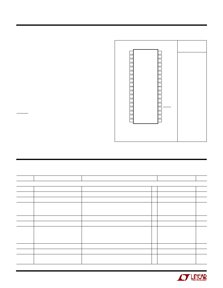
TOP VIEW
G PACKAGE
36-LEAD PLASTIC SSOP
36
35
34
33
32
31
30
29
28
27
26
25
24
23
22
21
20
19
PGOOD
TG1
SW1
BOOST1
V
IN
BG1
EXTV
CC
INTV
CC
PGND
BG2
BOOST2
SW2
TG2
RUN/SS2
AUXSD
AUXV
IN
AUXPGND
AUXPGND
RUN/SS1
SENSE1
+
SENSE1
≠
V
OSENSE1
FREQSET
STBYMD
FCB
I
TH1
SGND
3.3V
OUT
I
ITH2
V
OSENSE2
SENSE2
≠
SENSE2
+
AUXSGND
AUXV
FB
AUXSW
AUXSW
LTC1876
3
1876fa
SYMBOL
PARAMETER
CONDITIONS
MIN
TYP
MAX
UNITS
UVLO
Undervoltage Lockout
V
IN
Ramping Down
q
3.5
4
V
V
OVL
Overvoltage Feedback Threshold
Measured at V
OSENSE1, 2
q
0.84
0.86
0.88
V
I
SENSE
Sense Pins Total Source Current
(Each Channel); V
SENSE1
≠
, 2
≠
= V
SENSE1
+
, 2
+
= 0V
≠85
≠60
µ
A
V
STBYMD
MS
Master Shutdown Threshold
V
STBYMD
Ramping Down
0.4
0.6
V
V
STBYMD
KA
Keep-Alive Power On-Threshold
V
STBYMD
Ramping Up, RUN
SS1, 2
= 0V
1.5
2
V
DF
MAX
Maximum Duty Factor
In Dropout
98
99.4
%
I
RUN/SS1, 2
Soft-Start Charge Current
V
RUN/SS1, 2
= 1.9V
0.5
1.2
µ
A
V
RUN/SS1, 2
ON RUN/SS Pin ON Threshold
V
RUN/SS1,
V
RUN/SS2
Rising
1.0
1.5
1.9
V
V
RUN/SS1, 2
LT
RUN/SS Pin Latchoff Arming Threshold
V
RUN/SS1,
V
RUN/SS2
Rising from 3V
4.1
4.5
V
I
SCL1, 2
RUN/SS Discharge Current
Soft Short Condition V
OSENSE1, 2
= 0.5V;
0.5
2
4
µ
A
V
RUN/SS1, 2
= 4.5V
I
SDLHO
Shutdown Latch Disable Current
V
OSENSE1, 2
=0.5V
1.6
5
µ
A
V
SENSE(MAX)
Maximum Current Sense Threshold
V
OSENSE1, 2
= 0.7V
,
V
SENSE1
≠
, 2
≠
= 5V
q
62
75
88
mV
TG Transition Time:
TG1, 2 t
r
Rise Time
C
LOAD
= 3300pF
50
90
ns
TG1, 2 t
f
Fall Time
C
LOAD
= 3300pF
50
90
ns
BG Transition Time:
BG1, 2 t
r
Rise Time
C
LOAD
= 3300pF
40
90
ns
BG1, 2 t
f
Fall Time
C
LOAD
= 3300pF
40
80
ns
TG/BG t
1D
Top Gate Off to Bottom Gate On Delay
Synchronous Switch-On Delay Time
C
LOAD
= 3300pF Each Driver
90
ns
BG/TG t
2D
Bottom Gate Off to Top Gate On Delay
Top Switch-On Delay Time
C
LOAD
= 3300pF Each Driver
90
ns
t
ON(MIN)
Minimum ON-Time
Tested with a Square Wave (Note 7)
180
ns
INTV
CC
Linear Regulator
V
INTVCC
Internal V
CC
Voltage
6V < V
IN
< 30V, V
EXTVCC
= 4V
4.8
5.0
5.2
V
V
LDO
INT
INTV
CC
Load Regulation
I
CC
= 0 to 20mA, V
EXTVCC
= 4V
0.2
1.0
%
V
LDO
EXT
EXTV
CC
Voltage Drop
I
CC
= 20mA, V
EXTVCC
= 5V
80
160
mV
V
EXTVCC
EXTV
CC
Switchover Voltage
I
CC
= 20mA, EXTV
CC
Ramping Positive
q
4.5
4.7
V
V
LDOHYS
EXTV
CC
Hysteresis
0.2
V
Oscillator
f
OSC
Oscillator frequency
V
FREQSET
= Open (Note 8)
190
220
250
kHz
f
LOW
Lowest Frequency
V
FREQSET
= 0V
120
140
160
kHz
f
HIGH
Highest Frequency
V
FREQSET
= 2.4V
280
310
360
kHz
I
FREQSET
FREQSET
Input Current
V
FREQSET
= 2.4V
≠2
≠1
µ
A
ELECTRICAL CHARACTERISTICS
The
q
denotes the specifications which apply over the full operating
temperature range, otherwise specifications are at T
A
= 25
∞
C. V
IN
= 15V, V
RUN/SS1, 2
= 5V, AUXV
IN
= 3V unless otherwise noted.

LTC1876
4
1876fa
SYMBOL
PARAMETER
CONDITIONS
MIN
TYP
MAX
UNITS
3.3V Linear Regulator
V
3.3OUT
3.3V Regulator Output Voltage
No Load
q
3.25
3.35
3.45
V
V
3.3IL
3.3V Regulator Load Regulation
I
3.3
= 0mA to 10mA
0.5
2
%
V
3.3VL
3.3V Regulator Line Regulation
6V < V
IN
< 30V
0.05
0.2
%
PGOOD Output
V
PGL
PGOOD Voltage Low
I
PGOOD
= 2mA
0.1
0.3
V
I
PGOOD
PGOOD Leakage Current
V
PGOOD
= 5V
±
1
µ
A
V
PG
PGOOD Trip Level, Either Controller
V
OSENSE
with Respect to Set Output Voltage
V
OSENSE
Ramping Negative
≠6
≠7.5
≠9.5
%
V
OSENSE
Ramping Positive
6
7.5
9.5
%
Aux Output
AUXV
INMIN
AUX Minimum Operating Voltage
q
2.4
2.6
V
AUXV
FB
AUX Regulated Feedback Voltage
q
1.23
1.26
1.28
V
AUXI
FB
AUX Feedback Pin Bias Current
q
120
360
nA
AUXI
Q
AUX Input DC Supply Current
Normal Mode
V
AUXSD
= 2.4V, Not Switching
4
mA
Shutdown
V
AUXSD
= 0V
0.01
1
µ
A
AUXV
LINEREG
AUX Line Regulation
2.6V
AUXV
IN
16V
0.01
0.05
%/V
AUXf
OSC
AUX Oscillator Frequency
q
0.8
1.2
1.6
MHz
AUXDC
MAX
AUX Oscillator Maximum Duty Cycle
q
84
86
%
AUXI
LIMIT
AUX Switch Current Limit
(Note 9)
1
1.4
2
A
AUXV
CESAT
AUX Switch Saturation Voltage
I
SW
= 900mA (Note 10)
330
550
mV
AUXI
LEAKAGE
AUX Switch Leakage Current
V
SW
= 5V
0.01
1
µ
A
AUXV
AUXSD
AUX Shutdown Input Voltage
AUX Shutdown Upper Trip Point
2.4
V
AUX Shutdown Lower Trip Point
0.5
V
I
AUXSD
AUXSD Pin Bias Current
V
AUXSD
= 3V
16
32
µ
A
V
AUXSD
= 0V
0.01
0.1
µ
A
Note 1: Absolute Maximum Ratings are those values beyond which the life
of a device may be impaired.
Note 2: The LTC1876E is guaranteed to meet performance specifications
from 0
∞
C to 70
∞
C. Specifications over the ≠ 40
∞
C to 85
∞
C operating
temperature range are assured by design, characterization and correlation
with statistical process controls.
Note 3: T
J
is calculated from the ambient temperature T
A
and power
dissipation P
D
according to the following formulas:
LTC1876EG: T
J
= T
A
+ (P
D
∑ 95
∞
C/W)
Note 4: The LTC1876 is tested in a feedback loop that servos V
ITH1, 2
to a
specified voltage and measures the resultant V
OSENSE1, 2.
Note 5: Dynamic supply current is higher due to the gate charge being
delivered at the switching frequency. See Applications Information.
Note 6: Rise and fall times are measured using 10% and 90% levels.
Delay times are measured using 50% levels.
Note 7: The minimum on-time condition is specified for an inductor peak-
to-peak ripple current
40% of I
MAX
(see Minimum On-Time
Considerations in the Applications Information section).
Note 8: V
FREQSET
pin internally tied to 1.19V reference through a large
resistance.
Note 9: Current limit guaranteed by design and/or correlation to static test.
Note 10: 100% tested at wafer level.
ELECTRICAL CHARACTERISTICS
The
q
denotes the specifications which apply over the full operating
temperature range, otherwise specifications are at T
A
= 25
∞
C. V
IN
= 15V, V
RUN/SS1, 2
= 5V, AUXV
IN
= 3V unless otherwise noted.
LTC1876
5
1876fa
TYPICAL PERFOR A CE CHARACTERISTICS
U
W
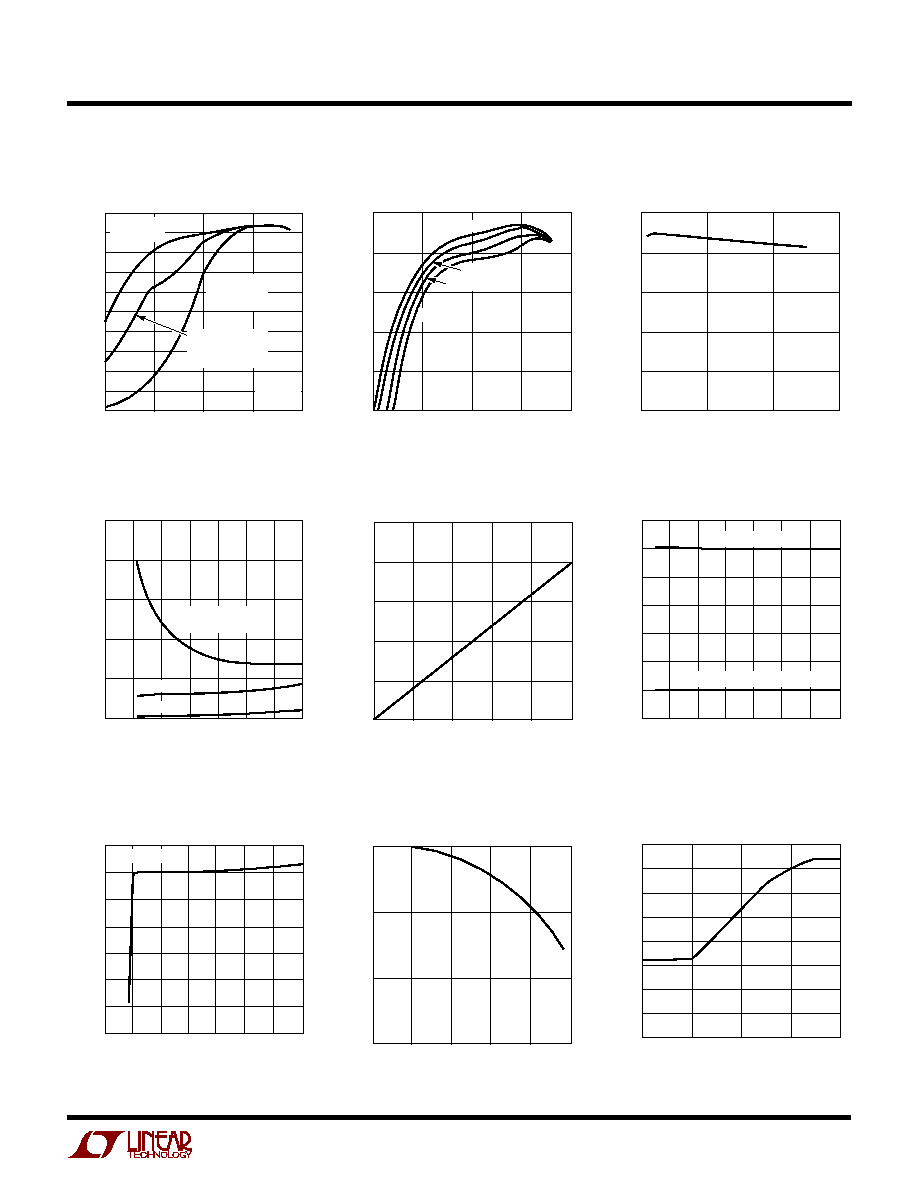
OUTPUT CURRENT (A)
0.001
0
EFFICIENCY (%)
10
30
40
50
100
70
0.01
0.1
1
1876 G01
20
80
90
60
10
FORCED
CONTINUOUS
MODE
CONSTANT
FREQUENCY
(BURST DISABLE)
Burst Mode
OPERATION
V
IN
= 15V
V
OUT
= 5V
OUTPUT CURRENT (A)
0.001
EFFICIENCY (%)
70
80
10
1876 G02
60
50
0.01
0.1
1
100
90
V
IN
= 10V
V
IN
= 15V
V
IN
= 7V
V
IN
= 20V
V
OUT
= 5V
INPUT VOLTAGE (V)
5
EFFICIENCY (%)
70
80
1876 G03
60
50
15
25
35
100
V
OUT
= 5V
I
OUT
= 3A
90
Efficiency vs Output Current and
Mode (Figure 1)
INPUT VOLTAGE (V)
0
5
0
SUPPLY CURRENT (
µ
A)
400
1000
10
20
25
1876 G04
200
800
600
15
30
35
BOTH
CONTROLLERS ON
STANDBY
SHUTDOWN
CURRENT (mA)
0
EXTV
CC
VOLTAGE DROP (mV)
150
200
250
40
1876 G05
100
50
0
10
20
30
50
TEMPERATURE (
∞
C)
≠ 50
INTV
CC
AND EXTV
CC
SWITCH VOLTAGE (V)
4.95
5.00
5.05
25
75
1876 G06
4.90
4.85
≠ 25
0
50
100
125
4.80
4.70
4.75
INTV
CC
VOLTAGE
EXTV
CC
SWITCHOVER THRESHOLD
INPUT VOLTAGE (V)
0
4.8
4.9
5.1
15
25
1876 G07
4.7
4.6
5
10
20
30
35
4.5
4.4
5.0
INTV
CC
VOLTAGE (V)
I
LOAD
= 1mA
Internal 5V LDO Line Regulation
V
IN
Supply Current vs Input
Voltage and Mode (Figure 1)
DUTY FACTOR (%)
0
0
V
SENSE
(mV)
25
50
75
20
40
60
80
1876 G08
100
PERCENT ON NOMINAL OUTPUT VOLTAGE (%)
0
V
SENSE
(mV)
40
50
60
100
1876 G09
30
20
0
25
50
75
10
80
70
Efficiency vs Output Current
(Figure 1)
Efficiency vs Input Voltage
(Figure 1)
EXTV
CC
Voltage Drop
INTV
CC
and EXTV
CC
Switch
Voltage vs Temperature
Maximum Current Sense
Threshold vs Duty Factor
Maximum Current Sense
Threshold vs Percent of Nominal
Output Voltage (Foldback)
LTC1876
6
1876fa
TYPICAL PERFOR A CE CHARACTERISTICS
U
W
V
RUN/SS
(V)
0
0
V
SENSE
(mV)
20
40
60
80
1
2
3
4
1876 G10
5
6
V
SENSE(CM)
= 1.6V
COMMON MODE VOLTAGE (V)
0
V
SENSE
(mV)
72
76
80
4
1876 G11
68
64
60
1
2
3
5
V
ITH
(V)
0
V
SENSE
(mV)
30
50
70
90
2
1876 G12
10
≠10
20
40
60
80
0
≠20
≠30
0.5
1
1.5
2.5
LOAD CURRENT (A)
0
NORMALIZED V
OUT
(%)
≠0.2
≠0.1
4
1876 G13
≠0.3
≠0.4
1
2
3
5
0.0
FCB = 0V
V
IN
= 15V
FIGURE 1
V
RUN/SS
(V)
0
0
V
ITH
(V)
0.5
1.0
1.5
2.0
2.5
1
2
3
4
1876 G14
5
6
V
OSENSE
= 0.7V
V
SENSE
COMMON MODE VOLTAGE (V)
0
I
SENSE
(
µ
A)
0
1876 G15
≠50
≠100
2
4
50
100
6
TEMPERATURE (
∞
C)
≠50
≠25
70
V
SENSE
(mV)
74
80
0
50
75
1876 G16
72
78
76
25
100
125
TEMPERATURE (
∞
C)
≠50
≠25
0
RUN/SS CURRENT (
µ
A)
0.2
0.6
0.8
1.0
75
100
50
1.8
1876 G18
0.4
0
25
125
1.2
1.4
1.6
Maximum Current Sense
Threshold vs V
RUN/SS
(Soft-Start)
Maximum Current Sense
Threshold vs Sense Common
Mode Voltage
Current Sense Threshold
vs I
TH
Voltage
Load Regulation (Controller)
V
ITH
vs V
RUN/SS
SENSE Pins Total Source Current
Maximum Current Sense
Threshold vs Temperature
Current Sense Pin Input Current
vs Temperature
RUN/SS Current vs Temperature
TEMPERATURE (
∞
C)
≠50
≠25
25
CURRENT SENSE INPUT CURRENT (
µ
A)
27
35
0
50
75
1876 G17
31
33
29
25
100
125
V
OUT
= 5V
LTC1876
7
1876fa
TEMPERATURE (
∞
C)
≠50
≠25
0
EXTV
CC
SWITCH RESISTANCE (
)
4
10
0
50
75
1876 G19
2
8
6
25
100
125
TEMPERATURE (
∞
C)
≠ 50
200
250
350
25
75
1876 G20
150
100
≠ 25
0
50
100
125
50
0
300
FREQUENCY (kHz)
V
FREQSET
= 5V
V
FREQSET
= OPEN
V
FREQSET
= 0V
TEMPERATURE (
∞
C)
≠50
UNDERVOLTAGE LOCKOUT (V)
3.40
3.45
3.50
25
75
1876 G21
3.35
3.30
≠25
0
50
100
125
3.25
3.20
TEMPERATURE (
∞
C)
≠50
≠25
0
SHUTDOWN LATCH THRESHOLDS (V) 0.5
1.5
2.0
2.5
75
100
50
4.5
1876 G22
1.0
0
25
125
3.0
3.5
4.0
LATCH ARMING
LATCHOFF
THRESHOLD
SHUTDOWN PIN VOLTAGE (V)
0
SHUTDOWN PIN CURRENT (
µ
A)
15
20
25
3
5
1876 G23
10
5
0
1
2
4
30
35
40
6
T
A
= 25
∞
C
T
A
= 100
∞
C
TEMPERATURE (
∞
C)
≠50
3.6
QUIESCENT CURRENT (mA)
3.8
3.9
4.0
4.1
4.2
4.3
0
50
1876 G24
4.4
4.5
4.6
3.7
100
V
IN
= 5V
V
FB
= 1.3V
NOT SWITCHING
V
IN
= 3.3V
TEMPERATURE (
∞
C)
≠50
1.22
FEEDBACK VOLTAGE (V)
1.23
1.24
1.25
1.26
1.28
≠25
0
25
50
1876 G25
75
100
1.27
TYPICAL PERFOR A CE CHARACTERISTICS
U
W
EXTV
CC
and Switch Resistance vs
Temperature
Undervoltage Lockout vs
Temperature (Controller)
Oscillator Frequency vs
Temperature (Controller)
Shutdown Latch Thresholds vs
Temperature
Shutdown Pin Current (I
AUXVFB
)
Quiescent Current for Auxillary
Regulator
Feedback Pin Voltage (AUXV
FB
)
Current Limit for Auxillary
Regulator
Auxillary Regulator Switch
Oscillator Frequency
TEMPERATURE (
∞
C)
≠50 ≠30 ≠10
1.05
FREQUENCY (MHz)
1.10
1.15
1.20
1.25
1.35
10
30
50
70
90
110
1876 G28
1.30
DUTY CYCLE (%)
10
CURRENT LI MIT (A)
0.8
1.2
90
1876 G26
0.4
0
30
50
70
20
40
60
80
1.6
0.6
1.0
0.2
1.4
LTC1876
8
1876fa
RUN/SS1, RUN/SS2 (Pins 1, 23): Combination of Soft-Start,
Run Control Inputs and Short-Circuit Detection Timers. A
capacitor to ground at each of these pins sets the ramp time
to full output current. Forcing either of these pins back below
1V causes the IC to shut down the circuitry required for that
particular controller. Latchoff overcurrent protection is also
invoked via this pin as described in the Applications Informa-
tion section.
SENSE1
+
, SENSE2
+
(Pins 2, 14): The (+) Input to each
Differential Current Comparator. The I
TH
pin voltage and
controlled offsets between the SENSE
≠
and SENSE
+
pins in
conjunction with R
SENSE
set the current trip threshold.
SENSE1
≠
, SENSE2
≠
(Pins 3, 13): The (≠) Input to the
Differential Current Comparators.
V
OSENSE1
, V
OSENSE2
(Pins 4, 12): Receives the remotely-
sensed feedback voltage for each controller from an external
resistive divider across the output.
FREQSET (Pin 5): Frequency Control Input to the Oscillator.
This pin can be left open, tied to ground, tied to INTV
CC
or
driven by an external voltage source. This pin can also be used
with an external phase detector to build a true phase-locked
loop.
STBYMD (Pin 6): Control pin that determines which circuitry
remains active when the controllers are shut down and/or
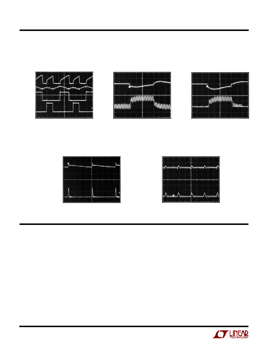
TYPICAL PERFOR A CE CHARACTERISTICS
U
W
PI
N
FU
N
CTIO
N
S
U
U
U
V
IN
= 15V
V
OUT
= 5V
LOAD STEP = 0A TO 3A
Burst Mode OPERATION
20
µ
s/DIV
1876 G30
V
OUT
200mV/DIV
I
OUT
2A/DIV
Load Step (Figure 1)
Constant Frequency (Burst
Inhibit) Operation (Figure 1)
Input Source/Capacitor
Instantaneous Current (Figure 1)
Burst Mode Operation (Figure 1)
I
IN
2A/DIV
V
IN
200mV/DIV
V
SW2
10V/DIV
V
IN
= 15V
V
OUT
= 5V
I
OUT5
= I
OUT3.3
= 2A
1
µ
s/DIV
1876 G31
V
SW1
10V/DIV
V
OUT
20mV/DIV
I
OUT
0.5A/DIV
V
IN
= 15V
V
OUT
= 5V
V
FCB
= OPEN
I
OUT
= 20mA
10
µ
s/DIV
1876 G32
V
OUT
20mV/DIV
I
OUT
0.5A/DIV
V
IN
= 15V
V
OUT
= 5V
V
FCB
= 5V
I
OUT
= 20mA
2
µ
s/DIV
1876 G33
V
IN
= 15V
V
OUT
= 5V
LOAD STEP = 0A TO 3A
CONTINUOUS MODE
Load Step (Figure 1)
V
OUT
200mV/DIV
I
OUT
2A/DIV

LTC1876
9
1876fa
provides a common control point to shut down both control-
lers. See the Operation section for details.
FCB (Pin 7): Forced Continuous Control Input. This input acts
on both controllers and is normally used to regulate a
secondary winding. Pulling this pin below 0.8V will force
continuous synchronous operation on both controllers. Do
not leave this pin floating.
I
TH1,
I
TH2
(Pins 8, 11): Error Amplifier Output and Switching
Regulator Compensation Point. Each associated channel's
current comparator trip point increases with this control
voltage.
SGND (Pin 9): Small signal ground common to both control-
lers, must be routed separately from high current grounds to
the common (≠) terminals of the C
OUT
capacitors.
3.3V
OUT
(Pin 10): Output of a linear regulator capable of
supplying up to 10mA DC with peak currents as high as
50mA.
AUXSGND (Pin 15): Small Signal Ground of the Auxiliary
Boost Regulator.
AUXV
FB
(Pin 16): Auxiliary Boost Regulator Feedback Volt-
age. This pin receives the feedback voltage from an external
resistive divider across the auxiliary output.
AUXSW (Pins 17, 18): Switch Node Connections to Inductor
for the Auxiliary Regulator. Voltage swing at these pins are
from ground to (V
OUT
+ voltage across Shottky diode).
Minimize trace area at these pins to keep EMI down.
AUXPGND (Pins 19, 20): The Auxiliary Power Ground Pins.
Its gate drive currents are returned to these pin.
AUXV
IN
(Pin 21): Auxiliary Boost Regulator Controller Sup-
ply Pin. Must be closely decoupled to AUXPGND.
AUXSD (Pin 22): Shutdown Pin for the Auxiliary Regulator.
Connect to 2.4V or more to enable the auxiliary regulator or
ground to shut the auxiliary regulator off.
TG1, TG2 (Pins 35, 24): High Current Gate Drives for Top
N-Channel MOSFETs. These are the outputs of floating
drivers with a voltage swing equal to INTV
CC
≠ 0.5V superim-
posed on the switch node voltage SW.
SW1, SW2 (Pins 34, 25): Switch Node Connections to
Inductors. Voltage swing at these pins is from a Schottky
diode (external) voltage drop below ground to V
IN
.
BOOST1, BOOST2 (Pins 33, 26): Bootstrapped Supplies to
the Top Side Floating Drivers. Capacitors are connected
between the boost and switch pins and Schottky diodes are
tied between the boost and INTV
CC
pins. Voltage swing at the
boost pins is from INTV
CC
to (V
IN
+ INTV
CC
).
BG1, BG2 (Pins 31, 27): High Current Gate Drives for Bottom
(synchronous) N-Channel MOSFETs. Voltage swing at these
pins is from ground to INTV
CC
.
PGND (Pin 28): Driver Power Ground. Connects to sources
of bottom (synchronous) N-channel MOSFETs, anode of the
Schottky rectifier and the (≠) terminal(s) of C
IN
.
INTV
CC
(Pin 29): Output of the Internal 5V Linear Low
Dropout Regulator and the EXTV
CC
Switch. The driver and
control circuits are powered from this voltage source. Must
be decoupled to power ground with a minimum of 4.7
µ
F
tantalum or other, low ESR capacitor. The INTV
CC
regulator
standby operation is determined by the STBYMD pin.
EXTV
CC
(Pin 30): External Power Input to an Internal Switch
Connected to INTV
CC
. This switch closes and supplies V
CC
power, bypassing the internal
low dropout regulator, when-
ever EXTV
CC
is higher than 4.7V. See EXTV
CC
connection in
Applications section. Do not exceed 7V on this pin.
V
IN
(Pin 32): Main Supply Pin. A bypass capacitor should be
tied between this pin and the signal ground pin.
PGOOD (Pin 36): Open-Drain Logic Output. PGOOD is pulled
to ground when the voltage on either V
OSENSE
pin is not within
7.5% of its setpoint.
PI
N
FU
N
CTIO
N
S
U
U
U
LTC1876
10
1876fa
FU
N
CTIO
N
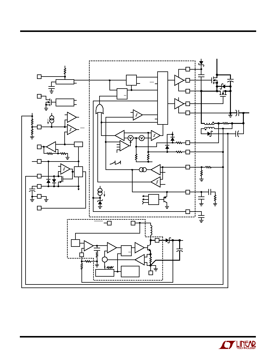
AL DIAGRA
U
U
W
SWITCH
LOGIC
≠
+
0.8V
4.8V
5V
V
IN
V
IN
4.5V
BINH
V
OSENSE1
V
OSENSE2
CLK2
CLK1
0.18
µ
A
R6
R5
+
≠
+
≠
+
≠
+
≠
FCB
+
≠
≠
+
≠
+
≠
+
V
REF
WINDOW
COMPARATOR
INTERNAL
SUPPLY
3.3V
OUT
V
SEC
FCB
PGOOD
EXTV
CC
INTV
CC
SGND
STBYMD
+
+
5V
LDO
REG
SW
SHDN
0.55V
TOP
BOOST
TG
C
B
C
IN
D
1
D
B
PGND
BOT
BG
INTV
CC
INTV
CC
V
IN
+
C
SEC
C
OUT
V
OUT
1876 FD/F02
D
SEC
R
SENSE
R2
+
V
OSENSE
DROP
OUT
DET
RUN
SOFT
START
BOT
TOP ON
S
R
Q
Q
S
Q
Q
OSCILLATOR
FREQSET
FCB
EA
0.86V
0.80V
OV
V
FB
1.2
µ
A
6V
R1
≠
+
R
C
4(V
FB
)
RST
SHDN
RUN/SS
I
TH
C
C
C
C2
C
SS
1.19V
1M
+
4(V
FB
)
0.86V
SLOPE
COMP
3mV
+
≠
≠
+
SENSE
≠
SENSE
+
INTV
CC
30k
45k
2.4V
45k
30k
I1
I2
B
DUPLICATE FOR SECOND
CONTROLLER CHANNEL
+
≠
≠
+
RUN/SS1
1.26V
V
REF
C
C
R
C
RAMP
GENERATOR
1.2MHz
OSCILLATOR
OSC
AUX
EA
AUX
A1
AUX
R
R7
R8
AUXSW
AUXSD
D5
L3
AUXV
FB
AUXV
OUT
AUXV
IN
C
OUTAUX
AUXPGND
BOOST
REGULATOR
Figure 2

LTC1876
11
1876fa
Main Control Loop
The LTC1876 uses a constant frequency, current mode
scheme to provide excellent line and load regulation for all
its outputs. The step-down controllers have two of its
switch drivers operating at 180 degrees out of phase from
each other. During normal operation, each top MOSFET is
turned on when the clock for that channel sets the R
S
latch,
and turned off when the main current comparator, I1,
resets the R
S
latch. The peak inductor current at which I1
resets the R
S
latch is controlled by the voltage on the I
TH
pin, which is the output of each error amplifier EA. The
V
OSENSE
pin receives the voltage feedback signal, which is
compared to the internal reference voltage by the EA.
When the load current increases, it causes a slight de-
crease in V
OSENSE
relative to the 0.8V reference, which in
turn causes the I
TH
voltage to increase until the average
inductor current matches the new load current. After the
top MOSFET has turned off, the bottom MOSFET is turned
on until either the inductor current starts to reverse, as
indicated by current comparator I2, or the beginning of the
next cycle.
The top MOSFET drivers are biased from floating boot-
strap capacitor C
B
, which normally is recharged during
each off cycle through an external diode when the top
MOSFET turns off. As V
IN
decreases to a voltage close to
V
OUT
, the loop may enter dropout and attempt to turn on
the top MOSFET continuously. The dropout detector de-
tects this and forces the top MOSFET off for about 500ns
every tenth cycle to allow C
B
to recharge.
The main control loop is shut down by pulling the RUN/SS
pin low. Releasing RUN/SS allows an internal 1.2
µ
A
current source to charge soft-start capacitor C
SS
. When
C
SS
reaches 1.5V, the main control loop is enabled with the
I
TH
voltage clamped at approximately 30% of its maximum
value. As C
SS
continues to charge, the I
TH
pin voltage is
gradually released allowing normal, full-current opera-
tion. When both RUN/SS1 and RUN/SS2 are low, all
LTC1876 controller functions are shut down, and the
STBYMD pin determines if the standby 5V and 3.3V
regulators are kept alive.
AUX Regulator
The auxiliary boost regulator is completely independent
from other LTC1876 circuits. It can be operated even
though the LTC1876 step-down controllers are in shut-
down. The operation of the boost regulator is similar to the
controllers. The oscillator, OSC
AUX
, sets the R
S
latch and
turns on the monolithic power switch. A voltage propor-
tional to the switch current is added to a stabilizing ramp
and the resulting sum is fed into the positive terminal of the
PWM comparator, A1
AUX
. When this voltage exceeds the
level at the negative input of A1
AUX
, the SR latch is reset,
turning off the power switch. The level at the negative input
of A1
AUX
is set by the error amplifier EA
AUX
and is simply
an amplified version of the difference between the feed-
back voltage and the reference voltage. Hence the error
amplifier sets the correct peak current level to keep the
output in regulation. To protect the power switch from
excessive current, a 1A minimum limit is internally set.
When the switch reaches this limit, it will force the latch to
reset, turning it off. Applying a voltage less than 0.5V on
the shutdown pin will put the boost regulator in shutdown.
Low Current Operation
The FCB pin is a multifunction pin providing two functions:
1) to provide regulation for a secondary winding by
temporarily forcing continuous PWM operation on both
controllers; and 2) select between
two modes of low
current operation. When the FCB pin voltage is below 0.8V,
the controller forces continuous PWM current operation.
In this mode, the top and bottom MOSFETs are alternately
turned on to maintain the output voltage independent of
direction of inductor current. When the FCB pin is below
V
INTVCC
≠ 2V but greater than 0.8V, the controller enters
Burst Mode operation. Burst Mode operation sets a mini-
mum output current level before turning off the top switch
and turns off the synchronous MOSFET(s) when the
inductor current goes negative. This combination of re-
quirements will, at low currents, force the I
TH
pin below a
voltage threshold that will temporarily inhibit turn-on of
both output MOSFETs until the output voltage drops
slightly. There is 60mV of hysteresis in the burst compara-
tor B tied to the I
TH
pin. This hysteresis produces output
signals to the MOSFETs that turn them on for several
(Refer to Functional Diagram)
OPERATIO
U

LTC1876
12
1876fa
cycles, followed by a variable "sleep" interval depending
upon the load current. The resultant output voltage ripple
is held to a very small value by having the hysteretic
comparator after the error amplifier gain block.
Constant Frequency Operation
When the FCB pin is tied to INTV
CC
, Burst Mode operation
is disabled and the forced minimum output current re-
quirement is removed. This provides constant frequency,
discontinuous (preventing reverse inductor current) cur-
rent operation over the widest possible output current
range. This constant frequency operation is not as efficient
as Burst Mode operation, but does provide a lower noise,
constant frequency operating mode down to approxi-
mately 1% of designed maximum output current.
Constant Current (PWM) Operation
Tying the FCB pin to ground will force continuous current
operation. This is the least efficient operating mode, but
may be desirable in certain applications. The output can
source or sink current in this mode. When sinking current
while in forced continuous operation, current will be
forced back into the main power supply potentially boost-
ing the input supply to dangerous voltage levels--
BEWARE!
Frequency Setting
The FREQSET pin provides frequency adjustment to the
controllers' internal oscillator from approximately 140kHz
to 310kHz. This input is nominally biased through an
internal resistor to the 1.19V reference, setting the oscil-
lator frequency to approximately 220kHz. This pin can be
driven from an external AC or DC signal source to control
the instantaneous frequency of the oscillator. The auxillary
boost regulator operates at a constant 1.2MHz frequency.
INTV
CC
/EXTV
CC
Power
Power for the top and bottom MOSFET drivers and most
other internal circuitry is derived from the INTV
CC
pin.
When the EXTV
CC
pin is left open, an internal 5V low
dropout linear regulator supplies INTV
CC
power. If EXTV
CC
is taken above 4.7V, the 5V regulator is turned off and an
internal switch is turned on connecting EXTV
CC
to INTV
CC
.
This allows the INTV
CC
power to be derived from a high
efficiency external source such as the output of the regu-
lator itself or a secondary winding, as described in Appli-
cations Information.
Standby Mode Pin
The STBYMD pin is a three-state input that controls
common circuitry within the IC as follows: When the
STBYMD pin is held at ground, both controller RUN/SS
pins are pulled to ground providing a single control pin to
shut down both controllers. When the pin is left open, the
internal RUN/SS currents are enabled to charge the
RUN/SS capacitor(s), allowing the turn-on of either con-
troller and activating necessary common internal biasing.
When the STBYMD pin is taken above 2V, both internal
linear regulators are turned on independent of the state of
the two switching regulator controllers, providing output
power to "wake-up" other circuitry. Decouple the pin with
a small capacitor (0.01
µ
F) to ground if the pin is not
connected to a DC potential.
Output Overvoltage Protection
An overvoltage comparator, OV, guards against transient
overshoots (>7.5%) as well as other more serious condi-
tions that may overvoltage the output. In this case, the top
MOSFET is turned off and the bottom MOSFET is turned on
until the overvoltage condition is cleared.
Power Good (PGOOD) Pin
The PGOOD pin is connected to an open drain of an internal
MOSFET. The MOSFET turns on and pulls the pin low when
both the outputs are not within
±
7.5% of their nominal
output levels as determined by their resistive feedback
dividers. When both controller outputs meet the
±
7.5%
requirement, the MOSFET is turned off within 10
µ
s and the
pin is allowed to be pulled up by an external resistor to a
source of up to 7V. The auxiliary regulator's output is not
monitored.
Foldback Current, Short-Circuit Detection and Short-
Circuit Latchoff
The RUN/SS capacitors are used initially to limit the inrush
current of each step-down switching regulator. After the
(Refer to Functional Diagram)
OPERATIO
U
LTC1876
13
1876fa
controller has been started and been given adequate time
to charge up the output capacitors and provide full-load
current, the RUN/SS capacitor is used as a short-circuit
time-out circuit. If the output voltage falls to less than 70%
of its nominal output voltage, the RUN/SS capacitor be-
gins discharging on the assumption that the output is in an
overcurrent and/or short-circuit condition. If the condition
lasts for a long enough period as determined by the size of
the RUN/SS capacitor, both controllers will be shut down
until the RUN/SS pin(s) voltage(s) are recycled. This built-
in latchoff can be overridden by providing a >5
µ
A pull-up
at a compliance of 5V to the RUN/SS pin(s). This current
shortens the soft start period but also prevents net dis-
charge of the RUN/SS capacitor(s) during an overcurrent
and/or short-circuit condition. Foldback current limiting is
also activated when the output voltage falls below 70% of
its nominal level whether or not the short-circuit latchoff
circuit is enabled. Even if a short is present and the short-
circuit latchoff is not enabled, a safe, low output current is
provided due to internal current foldback and actual power
wasted is low due to the efficient nature of the current
mode switching regulator.
Theory and Benefits of 2-Phase Operation
The LTC1876 dual high efficiency DC/DC controller brings
the considerable benefits of 2-phase operation to portable
applications for the first time. Notebook computers, PDAs,
handheld terminals and automotive electronics will all
benefit from the lower input filtering requirement, reduced
electromagnetic interference (EMI) and increased effi-
ciency associated with 2-phase operation.
Why the need for 2-phase operation? In most dual con-
stant-frequency switching regulators, both regulators are
operated in phase (i.e., single-phase operation). This
means that both switches turned on at the same time,
causing current pulses of up to twice the amplitude of
those for one regulator to be drawn from the input capaci-
tor and battery. These large amplitude current pulses
increased the total RMS current flowing from the input
capacitor, requiring the use of more expensive input
capacitors and increasing both EMI and losses in the input
capacitor and battery.
With 2-phase operation, the two channels of the dual-
switching regulator are operated 180 degrees out of
phase. This effectively interleaves the current pulses
coming from the switches, greatly reducing the overlap
time where they add together.
The result is a significant
reduction in total RMS input current, which in turn allows
less expensive input capacitors to be used, reduces shield-
ing requirements for EMI and improves real world operat-
ing efficiency.
Figure 3 compares the input waveforms for a representa-
tive single-phase dual switching regulator to the LTC1876
2-phase dual switching regulator. An actual measurement
of the RMS input current under these conditions shows
that 2-phase operation dropped the input current from
2.53A
RMS
to 1.55A
RMS
. While this is an impressive reduc-
tion in itself, remember that the power losses are propor-
tional to I
RMS
2
, meaning that the actual power wasted is
reduced by a factor of 2.66. The reduced input ripple
voltage also means less power is lost in the input power
(Refer to Functional Diagram)
OPERATIO
U
Figure 3. Input Waveforms Comparing Single-Phase (a) and 2-Phase (b) Operation for Dual Switching Regulators
Converting 12V to 5V and 3.3V at 3A Each. The Reduced Input Ripple with the LTC1876 2-Phase Regulator Allows
Less Expensive Input Capacitors, Reduces Shielding Requirements for EMI and Improves Efficiency
I
IN(MEAS)
= 2.53A
RMS
(a) Single-Phase
I
IN(MEAS)
= 1.55A
RMS
(b) 2-Phase
5V SWITCH
20V/DIV
1876 F03a
1876 F03b
3.3V SWITCH
20V/DIV
INPUT CURRENT
5A/DIV
INPUT VOLTAGE
500mV/DIV
5V SWITCH
20V/DIV
3.3V SWITCH
20V/DIV
INPUT CURRENT
5A/DIV
INPUT VOLTAGE
500mV/DIV
LTC1876
14
1876fa
path, which could include batteries, switches, trace/con-
nector resistances and protection circuitry. Improvements
in both conducted and radiated EMI also directly accrue as
a result of the reduced RMS input current and voltage.
Of course, the improvement afforded by 2-phase opera-
tion is a function of the dual switching regulator's relative
duty cycles which, in turn, are dependent upon the input
voltage V
IN
(Duty Cycle = V
OUT
/V
IN
). Figure 4 shows how
the RMS input current varies for single-phase and 2-phase
operation for 3.3V and 5V regulators over a wide input
voltage range.
It can readily be seen that the advantages of 2-phase
operation are not just limited to a narrow operating range,
but in fact extend over a wide region. A good rule of thumb
for most applications is that 2-phase operation will reduce
Allowing a margin for variations in the LTC1876 and
external component values yields:
R
mV
I
SENSE
MAX
=
50
Figure 4. RMS Input Current Comparison
(Refer to Functional Diagram)
OPERATIO
U
APPLICATIO S I FOR ATIO
W
U
U
U
Figure 1 on the first page is a basic LTC1876 application
circuit. For the step-down regulators, the external compo-
nent selection is driven by the load requirement, and
begins with the selection of R
SENSE
. Once R
SENSE
is
known, L can be chosen. Next, the power MOSFETs and D1
are selected. Finally, C
IN
and C
OUT
are selected . The circuit
shown in Figure 1 can be configured for operation up to an
input voltage of 28V (limited by the external MOSFETs).
For the step-up regulator, its component selection is much
simpler. A 4.7
µ
H or 10
µ
H inductor that can handle at least
1A without saturating will work well with most design. A
Shottky diode is recommended and a MBR0520 from ON
Semiconductor is a very good choice.
R
SENSE
Selection For Output Current
R
SENSE
is chosen based on the required output current.
The LTC1876 current comparator has a maximum thresh-
old of 75mV/R
SENSE
and an input common mode range of
SGND to 1.1(INTV
CC
). The current comparator threshold
sets the peak of the inductor current, yielding a maximum
average output current I
MAX
equal to the peak value less
half the peak-to-peak ripple current,
I
L
.
INPUT VOLTAGE (V)
0
INPUT RMS CURRENT (A)
3.0
2.5
2.0
1.5
1.0
0.5
0
10
20
30
40
1876 F04
SINGLE PHASE
DUAL CONTROLLER
2-PHASE
DUAL CONTROLLER
V
O1
= 5V/3A
V
O2
= 3.3V/3A
the input capacitor requirement to that for just one channel
operating at maximum current and 50% duty cycle.
OPERATING FREQUENCY (kHz)
120
170
220
270
320
FREQSET PIN VOLTAGE (V)
1876 F05
2.5
2.0
1.5
1.0
0.5
0
Figure 5. FREQSET Pin Voltage vs Frequency

LTC1876
15
1876fa
Selection of Operating Frequency
The LTC1876 uses a constant frequency architecture with
the frequency determined by an internal oscillator
capacitor. This internal capacitor is charged by a fixed
current plus an additional current that is proportional to
the voltage applied to the FREQSET pin.
A graph for the voltage applied to the FREQSET pin vs
frequency is given in Figure 5. As the operating frequency
is increased the gate charge losses will be higher, reducing
efficiency (see Efficiency Considerations). The maximum
switching frequency is approximately 310kHz.
Inductor Value Calculation
The operating frequency and inductor selection are inter-
related in that higher operating frequencies allow the use
of smaller inductor and capacitor values. So why would
anyone ever choose to operate at lower frequencies with
larger components? The answer is efficiency. A higher
frequency generally results in lower efficiency because of
MOSFET gate charge losses. In addition to this basic
trade-off, the effect of inductor value on ripple current and
low current operation must also be considered.
The inductor value has a direct effect on ripple current. The
inductor ripple current
I
L
decreases with higher induc-
tance or frequency and increases with higher V
IN
or V
OUT
:
I
f L
V
V
V
L
OUT
OUT
IN
=
1
1
( )( )
≠
Accepting larger values of
I
L
allows the use of low
inductances, but results in higher output voltage ripple
and greater core losses. A reasonable starting point for
setting ripple current is
I
L
=0.3(I
MAX
). Remember, the
maximum
I
L
occurs at the maximum input voltage.
The inductor value also has secondary effects. The transi-
tion to Burst Mode operation begins when the average
inductor current required results in a peak current below
25% of the current limit determined by R
SENSE
. Lower
inductor values (higher
I
L
) will cause this to occur at
lower load currents, which can cause a dip in efficiency in
the upper range of low current operation. In Burst Mode
operation, lower inductance values will cause the burst
frequency to decrease.
Inductor Core Selection
Once the value for L is known, the type of inductor must be
selected. High efficiency converters generally cannot af-
ford the core loss found in low cost powdered iron cores,
forcing the use of more expensive ferrite, molypermalloy,
or Kool M
µ
Æ
cores. Actual core loss is independent of core
size for a fixed inductor value, but it is very dependent on
inductance selected. As inductance increases, core losses
go down. Unfortunately, increased inductance requires
more turns of wire and therefore copper losses will in-
crease.
Ferrite designs have very low core loss and are preferred
at high switching frequencies, so design goals can con-
centrate on copper loss and preventing saturation. Ferrite
core material saturates "hard," which means that induc-
tance collapses abruptly when the peak design current is
exceeded. This results in an abrupt increase in inductor
ripple current and consequent output voltage ripple. Do
not allow the core to saturate!
Molypermalloy (from Magnetics, Inc.) is a very good, low
loss core material for toroids, but it is more expensive than
ferrite. A reasonable compromise from the same manu-
facturer is Kool M
µ
. Toroids are very space efficient,
especially when you can use several layers of wire. Be-
cause they generally lack a bobbin, mounting is more
difficult. However, designs for surface mount are available
that do not increase the height significantly.
Power MOSFET and D1 Selection
Two external power MOSFETs must be selected for each
controller with the LTC1876: One N-channel MOSFET for
the top (main) switch, and one N-channel MOSFET for the
bottom (synchronous) switch.
The peak-to-peak drive levels are set by the INTV
CC
volt-
age. This voltage is typically 5V during start-up (see
EXTV
CC
Pin Connection). Consequently, logic-level thresh-
old MOSFETs must be used in most applications. The only
exception is if low input voltage is expected (V
IN
< 5V);
APPLICATIO S I FOR ATIO
W
U
U
U
Kool M
µ
is a registered trademark of Magnetics, Inc.

LTC1876
16
1876fa
then, sub-logic level threshold MOSFETs (V
GS(TH)
< 3V)
should be used. Pay close attention to the BV
DSS
specifi-
cation for the MOSFETs as well; most of the logic level
MOSFETs are limited to 30V or less.
Selection criteria for the power MOSFETs include the "ON"
resistance R
DS(ON)
, reverse transfer capacitance C
RSS
,
input voltage and maximum output current. When the
LTC1876 is operating in continuous mode the duty cycles
for the top and bottom MOSFETs are given by:
Main Switch Duty Cycle
V
V
OUT
IN
=
Synchronous Switch Duty Cycle
V
V
V
IN
OUT
IN
=
≠
The MOSFET power dissipations at maximum output
current are given by:
P
V
V
I
R
k V
I
C
f
MAIN
OUT
IN
MAX
DS ON
IN
MAX
RSS
=
( )
+
( )
+
( ) ( )( )( )
2
2
1
(
)
P
V
V
V
I
R
SYNC
IN
OUT
IN
MAX
DS ON
=
( )
+
( )
≠
(
)
2
1
where
is the temperature dependency of R
DS(ON)
and k
is a constant inversely related to the gate drive current.
Both MOSFETs have I
2
R losses while the topside N-channel
equation includes an additional term for transition losses,
which are highest at high input voltages. For V
IN
< 20V the
high current efficiency generally improves with larger
MOSFETs, while for V
IN
> 20V the transition losses rapidly
increase to the point that the use of a higher R
DS(ON)
device
with lower C
RSS
actually provides higher efficiency. The
synchronous MOSFET losses are greatest at high input
voltage when the top switch duty factor is low or during a
short-circuit when the synchronous switch is on close to
100% of the period.
The term (1 +
) is generally given for a MOSFET in the
form of a normalized R
DS(ON)
vs temperature curve, but
= 0.005/
∞
C can be used as an approximation for low
voltage MOSFETs. C
RSS
is usually specified in the MOS-
FET characteristics. The constant k = 1.7 can be used to
estimate the contributions of the two terms in the main
switch dissipation equation.
The Schottky diode D1 shown in Figure 1 conducts during
the dead-time between the conduction of the two power
MOSFETs. This prevents the body diode of the bottom
MOSFET from turning on, storing charge during the dead-
time and requiring a reverse recovery period that could
cost as much as 3% in efficiency at high V
IN
. A 1A to 3A
Schottky is generally a good compromise for both regions
of operation due to the relatively small average current.
Larger diodes result in additional transition losses due to
their larger junction capacitance.
C
IN
Selection
The selection of C
IN
is simplified by the multiphase archi-
tecture and its impact on the worst-case RMS current
drawn through the input network (battery/fuse/capacitor).
It can be shown that the worst case RMS current occurs
when only one controller is operating. The controller with
the highest (V
OUT
)(I
OUT
) product needs to be used in the
formula below to determine the maximum RMS current
requirement. Increasing the output current, drawn from
the other out-of-phase controller, will actually decrease
the RMS ripple current from this maximum value (see
Figure 4). The out-of-phase technique typically reduces
the input capacitor's RMS ripple current by a factor of 30%
to 70% when compared to a single phase power supply
solution.
The type of input capacitor, value and ESR rating have
efficiency effects that need to be considered in the selec-
tion process. The capacitance value chosen should be
sufficient to store adequate charge to keep high peak
battery currents down. 20
µ
F to 40
µ
F is usually sufficient
for a 25W output supply operating at 200kHz. The ESR of
the capacitor is important for capacitor power dissipation
as well as overall battery efficiency. All of the power (RMS
ripple current ∑ ESR) not only heats up the capacitor but
wastes power from the battery.
APPLICATIO S I FOR ATIO
W
U
U
U
LTC1876
17
1876fa
Medium voltage (20V to 35V) ceramic, tantalum, OS-CON
and switcher-rated electrolytic capacitors can be used as
input capacitors, but each has drawbacks: ceramic voltage
coefficients are very high and may have audible piezoelec-
tric effects; tantalums need to be surge-rated; OS-CONs
suffer from higher inductance, larger case size and limited
surface-mount applicability; electrolytics' higher ESR and
dryout possibility require several to be used. Multiphase
systems allow the lowest amount of capacitance overall.
As little as one 22
µ
F or two to three 10
µ
F ceramic capaci-
tors are an ideal choice in a 20W to 35W power supply due
to their extremely low ESR. Even though the capacitance
at 20V is substantially below their rating at zero-bias, very
low ESR loss makes ceramics an ideal candidate for
highest efficiency battery operated systems. Also con-
sider parallel ceramic and high quality electrolytic capaci-
tors as an effective means of achieving ESR and bulk
capacitance goals.
In continuous mode, the source current of the top N-chan-
nel MOSFET is a square wave of duty cycle V
OUT
/V
IN
. To
prevent large voltage transients, a low ESR input capacitor
sized for the maximum RMS current of one channel must
be used. The maximum RMS capacitor current is given by:
C
quired I
I
V
V
V
V
IN
RMS
MAX
OUT
IN
OUT
IN
Re
/
-
(
)
[
]
1 2
This formula has a maximum at V
IN
= 2V
OUT
, where
I
RMS
= I
OUT
/2. This simple worst case condition is com-
monly used for design because even significant deviations
do not offer much relief. Note that capacitor manufacturer's
ripple current ratings are often based on only 2000 hours
of life. This makes it advisable to further derate the
capacitor, or to choose a capacitor rated at a higher
temperature than required. Several capacitors may also be
paralleled to meet size or height requirements in the
design. Always consult the manufacturer if there is any
question.
The benefit of the LTC1876 multiphase controllers can be
calculated by using the equation above for the higher
power controller and then calculating the loss that would
have resulted if both controller channels switch on at the
same time. The total RMS power lost is lower when both
controllers are operating due to the reduced overlap of
current pulses required through the input capacitor's ESR.
This is why the input capacitor's requirement calculated
above for the worst-case controller is adequate for the
dual controller design. Remember that protection fuse
resistance, battery resistance and PC board trace resis-
tance losses are also reduced due to the reduced peak
currents in a multiphase system.
The overall benefit of a
multiphase design will only be fully realized when the
source impedance of the power supply/battery is included
in the efficiency testing. The drains of the two top MOSFETS
should be placed within 1cm of each other and share a
common C
IN
(s). Separating the drains and C
IN
may pro-
duce undesirable voltage and current resonances at V
IN
.
For the boost regulator, the ripple requirement for the
input capacitor is less stringent. If the supply to the
regulator is obtained from one of the LTC1876 step-down
outputs, a 1
µ
F to 4.7
µ
F ceramic capacitor is sufficient.
However, if the step-down output is within close proximity
(< 1cm) to the boost supply input, there is no need for the
capacitor.
C
OUT
Selection
The selection of C
OUT
is driven by the required effective
series resistance (ESR). Typically once the ESR require-
ment is satisfied the capacitance is adequate for filtering.
For the step-down regulators, the output ripple (
V
OUT
) is
determined by:
V
I ESR
fC
OUT
L
OUT
+
1
8
Where f = operating frequency, C
OUT
= output capacitance,
and
L
= ripple current in the inductor. The output ripple is
highest at maximum input voltage since
I
L
increases
with input voltage. With
I
L
= 0.4I
OUT(MAX)
the output
ripple will typically be less than 50mV at max V
IN
assum-
ing:
C
OUT
Recommended ESR < 2 R
SENSE
and C
OUT
> 1/(8fR
SENSE
)
The first condition relates to the ripple current into the ESR
of the output capacitance while the second term guaran-
tees that the output capacitance does not significantly
APPLICATIO S I FOR ATIO
W
U
U
U

LTC1876
18
1876fa
discharge during the operating frequency period due to
ripple current. The choice of using smaller output capaci-
tance increases the ripple voltage due to the discharging
term but can be compensated for by using capacitors of
very low ESR to maintain the ripple voltage at or below
50mV. The I
TH
pin OPTI-LOOP compensation compo-
nents can be optimized to provide stable, high perfor-
mance transient response regardless of the output
capacitors selected.
For the boost regulator, the output ripple (
V
OUT
) is
determined by:
V
I
ESR
I
f C
OUT
PK
OUT
OUT
+
1 5
.
Since the boost regulator is operating at high frequency,
the second term will be small even with a small value of
C
OUT
. Hence, all efforts can be concentrated on finding a
low ESR capacitor. A ceramic capacitor can be used for the
output capacitor.
Manufacturers such as Nichicon, United Chemicon and
Sanyo can be considered for high performance through-
hole capacitors. The OS-CON semiconductor dielectric
capacitor available from Sanyo has the lowest (ESR) (size)
product of any aluminum electrolytic at a somewhat
higher price. An additional ceramic capacitor in parallel
with OS-CON capacitors is recommended to reduce the
inductance effects.
In surface mount applications multiple capacitors may
need to be used in parallel to meet the ESR, RMS current
handling and load step requirements of the application.
Aluminum electrolytic, dry tantalum and special polymer
capacitors are available in surface mount packages. Spe-
cial polymer surface mount capacitors offer very low ESR
but have lower storage capacity per unit volume than other
capacitor types. These capacitors offer a very cost-effec-
tive output capacitor solution and are an ideal choice when
combined with a controller having high loop bandwidth.
Tantalum capacitors offer the highest capacitance density
and are often used as output capacitors for switching
regulators having controlled soft-start. Several excellent
surge-tested choices are the AVX TPS, AVX TPSV or the
KEMET T510 series of surface mount tantalums, available
in case heights ranging from 2mm to 4mm. Aluminum
electrolytic capacitors can be used in cost-driven applica-
tions providing that consideration is given to ripple current
ratings, temperature and long term reliability. A typical
application will require several to many aluminum electro-
lytic capacitors in parallel. A combination of the above
mentioned capacitors will often result in maximizing per-
formance and minimizing overall cost. Other capacitor
types include Nichicon PL series, NEC Neocap, Pansonic
SP and Sprague 595D series. For high value of ceramic
capacitors, Taiyo Yuden has a series of them. Select the
X5R or X7R series as these retain the capacitance over
wide voltage and temperature range. Consult manufactur-
ers for other specific recommendations.
INTV
CC
Regulator
An internal P-channel low dropout regulator produces 5V
at the INTV
CC
pin from the V
IN
supply pin. INTV
CC
powers
the drivers and internal circuitry within the LTC1876 step-
down controllers. The INTV
CC
pin regulator can supply a
peak current of 50mA and must be bypassed to ground
with a minimum of 4.7
µ
F tantalum, 10
µ
F special polymer,
or low ESR type electrolytic capacitor. A 1
µ
F ceramic
capacitor placed directly adjacent to the INTV
CC
and PGND
IC pins is highly recommended. Good bypassing is neces-
sary to supply the high transient currents required by the
MOSFET gate drivers and to prevent interaction between
channels.
Higher input voltage applications in which large MOSFETs
are being driven at high frequencies may cause the maxi-
mum junction temperature rating for the LTC1876 to be
exceeded. The system supply current is normally domi-
nated by the gate charge current. Additional external
loading of the INTV
CC
and 3.3V linear regulators also
needs to be taken into account for the power dissipation
calculations. The total INTV
CC
current can be supplied by
either the 5V internal linear regulator or by the EXTV
CC
input pin. When the voltage applied to the EXTV
CC
pin is
less than 4.7V, all of the INTV
CC
current is supplied by the
internal 5V linear regulator. Power dissipation for the IC in
this case is highest: (V
IN
)(I
INTVCC
), and overall efficiency
is lowered. The gate charge current is dependent on
APPLICATIO S I FOR ATIO
W
U
U
U
LTC1876
19
1876fa
operating frequency as discussed in the Efficiency Consid-
erations section. The junction temperature can be esti-
mated by using the equations given in Note 3 of the
Electrical Characteristics. For example, the LTC1876 V
IN
current is limited to less than 24mA from a 24V supply
when not using the EXTV
CC
pin as follows:
T
J
= 70
∞
C + (24mA)(24V)(95
∞
C/W) = 125
∞
C
Use of the EXTV
CC
input pin reduces the junction tempera-
ture to:
T
J
= 70
∞
C + (24mA)(5V)(95
∞
C/W) = 81
∞
C
Dissipation should be calculated and added for current
drawn from the internal 3.3V linear regulator. To prevent
maximum junction temperature from being exceeded, the
input supply current must be checked operating in con-
tinuous mode at maximum V
IN
.
EXTV
CC
Connection
The LTC1876 contains an internal P-channel MOSFET
switch connected between the EXTV
CC
and INTV
CC
pins.
When the voltage applied to EXTV
CC
rises above
4.7V, the
internal regulator is turned off and the switch closes,
connecting the EXTV
CC
pin to the INTV
CC
pin thereby
supplying internal power. The switch remains closed as
long as the voltage applied to EXTV
CC
remains above 4.5V.
This allows the MOSFET driver and control power to be
derived from the output during normal operation (4.7V <
V
OUT
< 7V) and from the internal regulator when the output
is out of regulation (start-up, short-circuit). If more cur-
rent is required through the EXTV
CC
switch than is speci-
fied, an external Schottky diode can be added between the
EXTV
CC
and INTV
CC
pins. Do not apply greater than 7V to
the EXTV
CC
pin and ensure that EXTV
CC
< V
IN
.
Significant efficiency gains can be realized by powering
INTV
CC
from the output, since the V
IN
current resulting
from the driver and control currents will be scaled by a
factor of ((Duty Cycle)/efficiency). For 5V regulators this
supply means connecting the EXTV
CC
pin directly to V
OUT
.
However, for 3.3V and other lower voltage regulators,
additional circuitry is required to derive INTV
CC
power
from the output.
The following list summarizes the four possible connec-
tions for EXTV
CC
.
Make sure the voltage applied to the
EXTV
CC
does not exceed 7V.
1. EXTV
CC
Left Open (or Grounded). This will cause INTV
CC
to be powered from the internal 5V regulator resulting in
an efficiency penalty of up to 10% at high input voltages.
2. EXTV
CC
Connected directly to V
OUT
. This is the normal
connection for a 5V regulator and provides the highest
efficiency.
3. EXTV
CC
Connected to the output of the boost regulator.
If the LTC1876 auxillary boost regulator is set up for
output voltage between 4.7V and 7V, the EXTV
CC
can be
connected to this output.
4. EXTV
CC
Connected to an Output-Derived Boost Net-
work. For 3.3V and other low voltage regulators, efficiency
gains can still be realized by connecting EXTV
CC
to an
output-derived voltage that has been boosted to greater
than 4.7V. This can be done with either the inductive boost
winding as shown in Figure 6a or the capacitive charge
pump shown in Figure 6b. The charge pump has the
advantage of simple magnetics.
5. EXTV
CC
Connected to an External supply. If an external
supply is available in the 5V to 7V range, it may be used to
power EXTV
CC
providing it is compatible with the MOSFET
gate drive requirements.
APPLICATIO S I FOR ATIO
W
U
U
U
EXTV
CC
FCB
SGND
V
IN
TG1
SW
BG1
PGND
LTC1876
R
SENSE
V
OUT
V
SEC
+
C
OUT
+
1
µ
F
1876 F06a
N-CH
N-CH
R6
+
C
IN
V
IN
T1
1:N
OPTIONAL EXTV
CC
CONNECTION
5V < V
SEC
< 7V
R5
Figure 6a. Secondary Output Loop and EXTV
CC
Connection
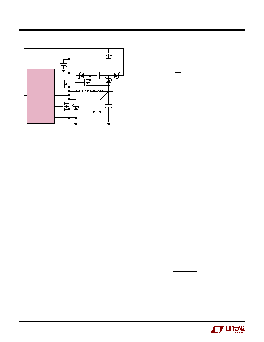
LTC1876
20
1876fa
Topside MOSFET Driver Supply (C
B
, D
B
)
External bootstrap capacitors C
B
connected to the BOOST
pins supply the gate drive voltages for the topside MOS-
FETs. Capacitor C
B
in the functional diagram is charged
though external diode D
B
from INTV
CC
when the SW pin is
low. When one of the topside MOSFETs is to be turned on,
the driver places the C
B
voltage across the gate-source of
the desired MOSFET. This enhances the MOSFET and
turns on the topside switch. The switch node voltage, SW,
rises to V
IN
and the BOOST pin follows. With the topside
MOSFET on, the boost voltage is above the input supply:
V
BOOST
= V
IN
+ V
INTVCC
. The value of the boost capacitor
C
B
needs to be 100 times that of the total input capacitance
of the topside MOSFET(s). The reverse breakdown of the
external Schottky diode must be greater than V
IN(MAX)
.
When adjusting the gate drive level, the final arbiter is the
total input current for the regulator. If a change is made
and the input current decreases, then the efficiency has
improved. If there is no change in input current, then there
is no change in efficiency.
Output Voltage
The LTC1876 output voltages are each set by an external
feedback resistive divider carefully placed across the
output capacitor as shown in Figure 2. For the step-down
controller, the resultant feedback signal is compared with
the internal precision 0.8V voltage reference by the error
amplifier. The output voltage is given by the equation:
V
V
R
R
OUT
=
+
0 8
1
2
1
.
For the auxillary boost regulator, the resultant feedback
signal is compared with the internal precision 1.26V
voltage reference by the error amplifier. The output volt-
age is given by the equation:
V
V
R
R
OUTAUX
=
+
1 26
1
8
7
.
SENSE
+
/SENSE
≠
Pins
The common mode input range of the current comparator
SENSE pins is from 0V to (1.1)INTV
CC
. Continuous linear
operation is guaranteed throughout this range allowing
output voltage setting from 0.8V to 7.7V, depending upon
the voltage applied to EXTV
CC
. A differential NPN input
stage is biased with internal resistors from an internal 2.4V
source as shown in the Functional Diagram. This requires
that current either be sourced or sunk from the SENSE
pins depending on the output voltage. If the output voltage
is below 2.4V current will flow out of both SENSE pins to
the main output. The output can be easily preloaded by the
V
OUT
resistive divider to compensate for the current
comparator's negative input bias current. The maximum
current flowing out of each pair of SENSE pins is:
I
SENSE
+
+ I
SENSE
≠
= (2.4V ≠ V
OUT
)/24k
Since V
OSENSE
is servoed to the 0.8V reference voltage, we
can choose R1 in Figure 2 to have a maximum value to
absorb this current.
R
k
V
V V
MAX
OUT
1
24
0 8
2 4
(
)
.
.
≠
=
for V
OUT
< 2.4V
Regulating an output voltage of 1.8V, the minimum value
of R1 should be 32k. Note that for an output voltage above
2.4V, R1 has no maximum value since the SENSE pins
load the output.
APPLICATIO S I FOR ATIO
W
U
U
U
EXTV
CC
V
IN
TG1
SW
BG1
PGND
LTC1876
R
SENSE
V
OUT
VN2222LL
+
C
OUT
1876 F06b
N-CH
N-CH
+
C
IN
+
1
µ
F
V
IN
L1
BAT85
BAT85
BAT85
0.22
µ
F
Figure 6b. Capacitive Charge Pump for EXTV
CC
LTC1876
21
1876fa
Soft-Start/Run Function
The RUN/SS1 and RUN/SS2 pins are multipurpose pins
that provide a soft-start function and a means to shut
down the LTC1876 step-down controllers. Soft-start re-
duces the input power source's surge currents by gradu-
ally increasing the controller's current limit (proportional
to V
ITH
). This pin can also be used for power supply
sequencing.
An internal 1.2
µ
A current source charges up the C
SS
capacitor
.
When the voltage on RUN/SS1 (RUN/SS2)
reaches 1.5V, the particular controller is permitted to start
operating. As the voltage on RUN/SS increases from 1.3V
to 3.0V, the internal current limit is increased from 25mV/
R
SENSE
to 75mV/R
SENSE
. The output current limit ramps
up slowly, taking an additional 1.2s/
µ
F to reach full cur-
rent. The output current thus ramps up slowly, reducing
the starting surge current required from the input power
supply. If RUN/SS has been pulled all the way to ground
there is a delay before starting of approximately:
t
V
A
C
s
F C
DELAY
SS
SS
=
µ
=
µ
(
)
1 5
1 2
1 25
.
.
.
/
t
V
V
A
C
s
F C
IRAMP
SS
SS
=
-
µ
=
µ
(
)
3
1 5
1 2
1 25
.
.
.
/
By pulling both RUN/SS pins below 1.0V and/or pulling the
STBYMD pin below 0.2V, the controllers are put into low
current shutdown (I
Q
= 20
µ
A). The RUN/SS pins can be
driven directly from logic as shown in Figure 7. Diode D1
in Figure 7 reduces the start delay but allows C
SS
to ramp
up slowly providing the soft-start function. Each RUN/SS
pin has an internal 6V Zener clamp (See Functional Dia-
gram).
Fault Conditions: Overcurrent Latchoff
The RUN/SS pins also provide the ability to latch off the
controller(s) when an overcurrent condition is detected.
The RUN/SS capacitor, C
SS
, is used initially to turn on and
limit the inrush current of the controller. After the control-
ler has been started and been given adequate time to
charge up the output capacitor and provide full load
current, the RUN/SS capacitor is used for a short-circuit
timer. If the regulator's output voltage falls to less than
70% of its nominal value after C
SS
reaches 4.1V, C
SS
begins discharging on the assumption that the output is in
an overcurrent condition. If the condition lasts for a long
enough period as determined by the size of the C
SS
and the
specified discharge current, the controller will be shut
down until the RUN/SS pin voltage is recycled. If the
overload occurs during start-up, the time can be approxi-
mated by:
T
LO1
[C
SS
(4.1 ≠ 1.5 + 4.1 ≠ 3.5)]/(1.2
µ
A)
= 2.7 ∑ 10
6
(C
SS
)
If the overload occurs after start-up the voltage on C
SS
will
begin discharging from the zener clamp voltage:
T
LO2
[C
SS
(6 ≠ 3.5)]/(1.2
µ
A) = 2.1 ∑ 10
6
(C
SS
)
If an overload occurs on one channel, it will also latch off
the other channel. This built-in overcurrent latchoff can be
overridden by providing a pull-up resistor to the RUN/SS
pin as shown in Figure 7. This resistance shortens the soft-
start period and prevents the discharge of the RUN/SS
capacitor during an over current condition. Tying this pull-
up resistor to V
IN
as in Figure 7a, defeats overcurrent
latchoff. Diode-connecting this pull-up resistor to INTV
CC
,
as in Figure 7b, eliminates any extra supply current during
controller shutdown while eliminating the INTV
CC
loading
from preventing controller start-up.
Why should you defeat overcurrent latchoff? During the
prototype stage of a design, there may be a problem with
noise pickup or poor layout causing the protection circuit
to latch off. Defeating this feature will easily allow trouble-
shooting of the circuit and PC layout. The internal short-
circuit and foldback current limiting still remains active,
thereby protecting the power supply system from failure.
After the design is complete, a decision can be made
whether to enable the latchoff feature.
APPLICATIO S I FOR ATIO
W
U
U
U
Figure 7. RUN/SS Pin Interfacing
3.3V OR 5V
RUN/SS
V
IN
INTV
CC
RUN/SS
D1
C
SS
R
SS
*
C
SS
R
SS
*
1876 F07
(a)
(b)
*OPTIONAL TO DEFEAT OVERCURRENT LATCHOFF
LTC1876
22
1876fa
The value of the soft-start capacitor C
SS
may need to be
scaled with output voltage, output capacitance and load
current characteristics. The minimum soft-start capaci-
tance is given by:
C
SS
> (C
OUT
)(V
OUT
) (10
≠4
) (R
SENSE
)
The minimum recommended soft-start capacitor of
C
SS
= 0.1
µ
F will be sufficient for most applications.
Fault Conditions: Current Limit and Current Foldback
The LTC1876 step-down controllers current comparator
has a maximum sense voltage of 75mV resulting in a
maximum MOSFET current of 75mV/R
SENSE
. The maxi-
mum value of current limit generally occurs with the
largest V
IN
at the highest ambient temperature, conditions
that cause the highest power dissipation in the top MOSFET.
The controllers include current foldback to help further
limit load current when the output is shorted to ground.
The foldback circuit is active even when the overload
shutdown latch described above is overridden. If the
output falls below 70% of its nominal output level, then the
maximum sense voltage is progressively lowered from
75mV to 25mV. Under short-circuit conditions with very
low duty cycles, the step-down regulators will begin cycle
skipping in order to limit the short-circuit current. In this
situation the bottom MOSFET will be dissipating most of
the power but less than in normal operation. The short-
circuit ripple current is determined by the minimum on-
time t
ON(MIN)
(less than 200ns), the input voltage and
inductor value:
I
L(SC)
= t
ON(MIN)
(V
IN
/L)
The resulting short-circuit current is:
I
mV
R
I
SC
SENSE
L SC
=
+
25
1
2
(
)
Fault Conditions: Overvoltage Protection (Crowbar)
The overvoltage crowbar is designed to blow a system
input fuse when the output voltage of the step-down
regulator rises much higher than nominal levels. The
crowbar causes huge currents to flow, that blow the fuse
to protect against a shorted top MOSFET if the short
occurs while the controller is operating.
A comparator monitors the output for overvoltage condi-
tions. The comparator (OV) detects overvoltage faults
greater than 7.5% above the nominal output voltage.
When this condition is sensed, the top MOSFET is turned
off and the bottom MOSFET is turned on until the overvolt-
age condition is cleared. The output of this comparator is
only latched by the overvoltage condition itself and will
therefore allow a switching regulator system having a poor
PC layout to function while the design is being debugged.
The bottom MOSFET remains on continuously for as long
as the OV condition persists; if V
OUT
returns to safe level,
normal operation automatically resumes. A shorted top
MOSFET will result in a high current condition which will
open the system fuse. The switching regulator will regu-
late properly with a leaky top MOSFET by altering the duty
cycle to accommodate the leakage.
The Standby Mode (STBYMD) Pin Function
The Standby Mode (STBYMD) pin provides several choices
for start-up and standby operational modes. If the pin is
pulled to ground, the RUN/SS pins for both controllers are
internally pulled to ground, preventing start-up and thereby
providing a single control pin for turning off both control-
lers at once. If the pin is left open or decoupled with a
capacitor to ground, the RUN/SS pins are each internally
provided with a starting current enabling external control
for turning on each controller independently. If the pin is
provided with a current of >3
µ
A at a voltage greater than
2V, both internal linear regulators (INTV
CC
and 3.3V) will
be on even when both controllers are shut down. In this
mode, the onboard 3.3V and 5V linear regulators can
provide power to keep-alive functions such as a keyboard
controller. This pin can also be used as a latching "on" and/
or latching "off" power switch if so designed.
Frequency of Operation
The LTC1876 stepdown controllers have an internal volt-
age controlled oscillator. The frequency of this oscillator
can be varied over a 2 to 1 range. The pin is internally self-
biased at 1.19V, resulting in a free-running frequency of
APPLICATIO S I FOR ATIO
W
U
U
U
LTC1876
23
1876fa
approximately 220kHz. The FREQSET pin can be grounded
to lower this frequency to approximately 140kHz or tied to
the INTV
CC
pin to yield approximately 310kHz. The FREQSET
pin may be driven with a voltage from 0 to INTV
CC
to fix or
modulate the oscillator frequency as shown in Figure 5.
Minimum On-Time Considerations
Minimum on-time t
ON(MIN)
is the smallest time duration
that the step down controller is capable of turning on the
top MOSFET. It is determined by internal timing delays and
the gate charge required to turn on the top MOSFET. Low
duty cycle applications may approach this minimum on-
time limit and care should be taken to ensure that.
t
V
V f
ON MIN
OUT
IN
(
)
( )
<
If the duty cycle falls below what can be accommodated by
the minimum on-time, the controller will begin to skip
cycles. The output voltage will continue to be regulated,
but the ripple voltage and current will increase.
The minimum on-time for each controller is generally less
than 200ns. However, as the peak sense voltage decreases
the minimum on-time gradually increases up to about
300ns. This is of particular concern in forced continuous
applications with low ripple current at light loads. If the
duty cycle drops below the minimum on-time limit in this
situation, a significant amount of cycle skipping can occur
with correspondingly larger current and voltage ripple.
FCB Pin Operation
The FCB pin can be used to regulate a secondary winding
or as a logic level input. Continuous operation is forced
when the FCB pin drops below 0.8V. During continuous
mode, current flows continuously in the transformer pri-
mary. The secondary winding(s) draw current only when
the bottom, synchronous switch is on. When primary load
currents are low and/or the V
IN
/V
OUT
ratio is low, the
synchronous switch may not be on for a sufficient amount
of time to transfer power from the output capacitor to the
secondary load. Forced continuous operation will support
secondary windings providing there is sufficient
synchronous switch duty factor. Thus, the FCB input pin
removes the requirement that power must be drawn from
the inductor primary in order to extract power from the
auxiliary windings. With the loop in continuous mode, the
auxiliary outputs may nominally be loaded without regard
to the primary output load.
The secondary output voltage V
SEC
is normally set as
shown in Figure 6a by the turns ratio N of the transformer:
V
SEC
(N + 1) V
OUT
However, if the controller goes into Burst Mode operation
and halts switching due to a light primary load current,
then V
SEC
will droop. An external resistive divider from
V
SEC
to the FCB pin sets a minimum voltage V
SEC(MIN)
:
V
V
R
R
SEC MIN
(
)
.
+
0 8
1
6
5
If V
SEC
drops below this level, the FCB voltage forces
temporary continuous switching operation until V
SEC
is
again above its minimum.
In order to prevent erratic operation if no external connec-
tions are made to the FCB pin, the FCB pin has a 0.18
µ
A
internal current source pulling the pin high. Include this
current when choosing resistor values R5 and R6.
The following table summarizes the possible states avail-
able on the FCB pin:
Table 1
FCB Pin
Condition
0V to 0.75V
Forced Continuous (Current Reversal
Allowed--Burst Inhibited)
0.85V < V
FB
< 4.3V
Minimum Peak Current Induces
Burst Mode Operation
No Current Reversal Allowed
Feedback Resistors
Regulating a Secondary Winding
>4.8V
Burst Mode Operation Disabled
Constant Frequency Mode Enabled
No Current Reversal Allowed
No Minimum Peak Current
Remember that both controllers are temporarily forced
into continuous mode when the FCB pin falls below 0.8V.
APPLICATIO S I FOR ATIO
W
U
U
U

LTC1876
24
1876fa
Voltage Positioning
Voltage positioning can be used to minimize peak-to-peak
output voltage excursions under worst-case transient
loading conditions. The open loop DC gain of the control
loop is reduced depending upon the maximum load step
specifications. Voltage positioning can be easily added to
the LTC1876 by loading the I
TH
pin with a resistive divider
having a Thevenin equivalent voltage source equal to the
midpoint operating voltage of the error amplifier, or 1.2V
(see Figure 8).
The resistive load reduces the DC loop gain while main-
taining the linear control range of the error amplifier. The
maximum output voltage deviation can theoretically be
reduced to half or alternatively the amount of output
capacitance can be reduced for a particular application. A
complete explanation is included in Design Solutions 10.
(See: www.linear-tech.com)
1. The V
IN
current has two components: the first is the DC
supply current given in the Electrical Characteristics table,
which excludes MOSFET driver and control currents; the
second is the current drawn from the 3.3V linear regulator
output. V
IN
current typically results in a small (<0.1%)
loss.
2. INTV
CC
current is the sum of the MOSFET driver and
control currents. The MOSFET driver current results from
switching the gate capacitance of the power MOSFETs.
Each time a MOSFET gate is switched from low to high to
low again, a packet of charge dQ moves from INTV
CC
to
ground. The resulting dQ/dt is a current out of INTV
CC
that
is typically much larger than the control circuit current. In
continuous mode, I
GATECHG
=f(Q
T
+Q
B
), where Q
T
and Q
B
are the gate charges of the topside and bottom side
MOSFETs.
Supplying INTV
CC
power through the EXTV
CC
switch input
from an output-derived source will scale the V
IN
current
required for the driver and control circuits by a factor of
(Duty Cycle)/(Efficiency). For example, in a 20V to 5V
application, 10mA of INTV
CC
current results in approxi-
mately 3mA of V
IN
current. This reduces the mid-current
loss from 10% or more (if the driver was powered directly
from V
IN
) to only a few percent.
3. I
2
R losses are predicted from the DC resistances of the
fuse (if used), MOSFET, inductor, current sense resistor,
and input and output capacitor ESR. In continuous mode
the average output current flows through L and R
SENSE
,
but is "chopped" between the topside MOSFET and the
synchronous MOSFET. If the two MOSFETs have approxi-
mately the same R
DS(ON)
, then the resistance of one
MOSFET can simply be summed with the resistances of L,
R
SENSE
and ESR to obtain I
2
R losses. For example, if each
R
DS(ON)
= 30m
, R
L
= 50m
, R
SENSE
= 10m
and R
ESR
= 40m
(sum of both input and output capacitance
losses), then the total resistance is 130m
. This results in
losses ranging from 3% to 13% as the output current
increases from 1A to 5A for a 5V output, or a 4% to 20%
loss for a 3.3V output. Efficiency varies as the inverse
square of V
OUT
for the same external components and
output power level. The combined effects of increasingly
lower output voltages and higher currents required by
high performance digital systems is not doubling but
APPLICATIO S I FOR ATIO
W
U
U
U
I
TH
R
C
R
T1
INTV
CC
C
C
1876 F08
LTC1876
R
T2
Efficiency Considerations
The percent efficiency of a switching regulator is equal to
the output power divided by the input power times 100%.
It is often useful to analyze individual losses to determine
what is limiting the efficiency and which change would
produce the most improvement. Percent efficiency can be
expressed as:
%Efficiency = 100% ≠ (L1 + L2 + L3 + ...)
where L1, L2, etc. are the individual losses as a percentage
of input power.
Although all dissipative elements in the circuit produce
losses, four main sources usually account for most of the
losses in LTC1876 circuits: 1) LTC1876 V
IN
current (in-
cluding loading on the 3.3V internal regulator), 2) INTV
CC
regulator current, 3) I
2
R losses, 4) topside MOSFET
transition losses.
Figure 8. Active Voltage Positioning Applied to the LTC1876

LTC1876
25
1876fa
quadrupling the importance of loss terms in the switching
regulator system!
4. Transition losses apply only to the topside MOSFET(s),
and only when operating at high input voltages (typically
20V or greater). Transition losses can be estimated from:
Transition Loss = (1.7) V
IN
2
I
O(MAX)
C
RSS
f
Other "hidden" losses such as copper trace and internal
battery resistances can account for an additional 5% to
10% efficiency degradation in portable systems. It is very
important to include these "system" level losses in the
design of a system. The internal battery and fuse resis-
tance losses can be minimized by making sure that C
IN
has
adequate charge storage and very low ESR at the switch-
ing frequency. A 25W supply will typically require a
minimum of 20
µ
F to 40
µ
F of capacitance having a maxi-
mum of 20m
to 50m
of ESR. The LTC1876 step-down
controllers 2-phase architecture typically halves this input
capacitance requirement over competing solutions. Other
losses including Schottky conduction losses during dead-
time and inductor core losses generally account for less
than 2% total additional loss.
Checking Transient Response
The regulator loop response can be checked by looking at
the load current transient response. Switching regulators
take several cycles to respond to a step in DC (resistive)
load current. When a load step occurs, V
OUT
shifts by an
amount equal to
I
LOAD
(ESR), where ESR is the effective
series resistance of C
OUT
.
I
LOAD
also begins to charge or
discharge C
OUT
generating the feedback error signal that
forces the regulator to adapt to the current change and
return V
OUT
to its steady-state value. During this recovery
time V
OUT
can be monitored for excessive overshoot or
ringing, which would indicate a stability problem. OPTI-
LOOP compensation allows the transient response to be
optimized over a wide range of output capacitance and
ESR values.
The availability of the I
TH
pin not only allows
optimization of control loop behavior but also provides a
DC coupled and AC filtered closed loop response test
point. The DC step, rise time and settling at this test point
truly reflects the closed loop response. Assuming a pre-
dominantly second order system, phase margin and/or
damping factor can be estimated using the percentage of
overshoot seen at this pin. The bandwidth can also be
estimated by examining the rise time at the pin. The I
TH
external components shown in the Figure 1 circuit will
provide an adequate starting point for most applications.
The I
TH
series R
C
-C
C
filter sets the dominant pole-zero
loop compensation. The values can be modified slightly
(from 0.5 to 2 times their suggested values) to maximize
transient response once the final PC layout is done and the
particular output capacitor type and value have been
determined. The output capacitors need to be selected
because the various types and values determine the loop
feedback factor gain and phase. An output current pulse of
20% to 100% of full-load current having a rise time of 1
µ
s
to 10
µ
s will produce output voltage and I
TH
pin waveforms
that will give a sense of the overall loop stability without
breaking the feedback loop. The initial output voltage step
resulting from the step change in output current may not
be within the bandwidth of the feedback loop, so this signal
cannot be used to determine phase margin. This is why it
is better to look at the I
TH
pin signal which is in the
feedback loop and is the filtered and compensated control
loop response. The gain of the loop will be increased by
increasing R
C
and the bandwidth of the loop will be
increased by decreasing C
C
. If R
C
is increased by the same
factor that C
C
is decreased, the zero frequency will be kept
the same, thereby keeping the phase the same in the most
critical frequency range of the feedback loop. The output
voltage settling behavior is related to the stability of the
closed-loop system and will demonstrate the actual over-
all supply performance.
A second, more severe transient is caused by switching in
loads with large (>1
µ
F) supply bypass capacitors. The
discharged bypass capacitors are effectively put in parallel
with C
OUT
, causing a rapid drop in V
OUT
. No regulator can
alter its delivery of current quickly enough to prevent this
sudden step change in output voltage if the load switch
resistance is low and it is driven quickly. If the ratio of
C
LOAD
to C
OUT
is greater than 1:50, the switch rise time
should be controlled so that the load rise time is limited to
approximately 25 ∑ C
LOAD
. Thus a 10
µ
F capacitor would
require a 250
µ
s rise time, limiting the charging current to
about 200mA.
APPLICATIO S I FOR ATIO
W
U
U
U
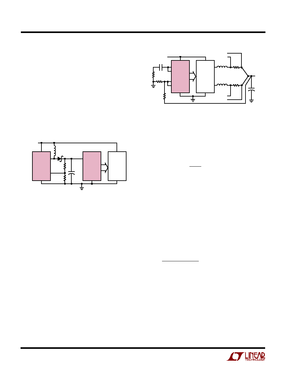
LTC1876
26
1876fa
Low V
IN
Applications
In applications where the input supply is low (<5V), the
LTC1876 auxiliary regulator can be used to step-up the
input to provide the gate drive to the external MOSFETs as
shown in Figure 9.
Shown in the Typical Application section of the data sheet
is a circuit (3.3V
IN
Dual-Phase High Efficiency Power
Supply) with input supply of 3.3V. The boost section of the
LTC1876 is set up to generate 5V and is used to provide the
gate drive to the external MOSFETs. The circuit provides
dual outputs, a 2.5V/15A and 1.8V/15A. Both drawing
power directly from V
IN
.
APPLICATIO S I FOR ATIO
W
U
U
U
Figure 9. Generating the Gate Drive
for Low Input Supply Applications
Figure 10. Single Output Configuration
Single Output/High Current Applications
In applications that demand current much higher than a
single stage can supply (>20A), the LTC1876 can be
configured as a single output converter. Figure 10 shows
the block diagram of the configuration. Note that the
compensation pins (I
TH1
and I
TH2
) of the two channels are
connected together, saving a set of passive components.
In addition, the output voltage sense pins (V
OSENSE1
and
V
OSENSE2
) are shorted together, using only one resistor
divider to set the output voltage.
Although the output current requirement is high, the input
capacitors ripple current requirement is not much differ-
ent compared to the dual outputs circuit. This is attributed
to the fact that the current is shared between two channels
and an out-of-phase architecture is implemented for the
controllers
(See Theory and Benefits of 2-Phase
Operation).
Auxiliary Regulator's Inductor Value Calculation
Since the current limit for the auxiliary regulator is inter-
nally set at 1A, it makes the selection of components
easier. For the boost regulator, the duty cycle is given by:
Duty Cycle
V
V
IN
OUT
=
1≠
Since energy is only transferred to the output capacitor(s)
during the off-time, the maximum output current that can
be supplied by the regulator without losing regulation is:
I
OUT
= 0.5(2 ∑ I
PK
≠
I
L
)(1 ≠ Duty Cycle)
where I
PK
= peak inductor current and is internally set at
1A.
I
L
= inductor's ripple current
With the required ripple current determined, the value of
the inductor is:
L
V
Duty Cycle
f
I
IN
L
=
(
∑
)
( ∑
)
where f = operating frequency (1.2MHz)
In most cases, a larger value of inductance is used. This is
done to account for component variation. It also lowers
the inductor ripple current and results in lower core
losses. In addition, lower ripple also translates into lower
ESR losses in the output capacitors and smaller output
voltage ripple.
1876 F09
LTC1876
BOOST
SECTION
LTC1876
STEP-DOWN
SECTION
AUXV
IN
AUXSW
AUXV
FB
SGND
+
EXTERNAL
MOSFETs
L1
V
IN
C
OUT
R7
R8
D1
INPUT
SUPPLY
1876 F10
LTC1876
SGND
EXTERNAL
MOSFETs
V
IN
V
OUT
INPUT
SUPPLY
I
TH1
I
TH2
V
OSENSE1
V
OSENSE2
TO SENSE1
+
AND SENSE1
≠
TO SENSE2
+
AND SENSE2
≠
L1
L2
R2
R1
R
S1
R
S2
+
C
C
R
C
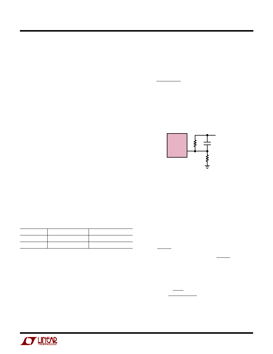
LTC1876
27
1876fa
Once the value of L is known, select an inductor that can
handle at least 1A without saturating. In addition, ensure
that the inductor has a low DCR (copper wire resistance)
to minimize I
2
R power losses.
Auxiliary Regulator's Capacitor Selection
Low ESR (equivalent series resistance) capacitors should
be used at the output to minimize the output ripple voltage.
Multilayer ceramic capacitors are an excellent choice, as
they have extremely low ESR and are available in very
small packages. X5R dielectrics are preferred, followed by
X7R, as these materials retain the capacitance over wide
voltage and temperature ranges. A 4.7
µ
F to 10
µ
F output
capacitor is sufficient for most applications, but systems
with very low output current may need only a 1
µ
F or 2.2
µ
F
output capacitor. Solid tantalum or OS-CON capacitors
can be used, but they will occupy more board area than a
ceramic and will have a higher ESR. Always use a capacitor
with a sufficient voltage rating.
Ceramic capacitors also make a good choice for the input
decoupling capacitor, and should be placed as close as
possible to the AUXV
IN
pin. A 1
µ
F to 4.7
µ
F input capacitor
is sufficient for most applications. Table 2 shows a list of
several ceramic capacitor manufacturers. Consult the
manufacturers for detailed information on their entire
selection of ceramic parts.
Table 2. Ceramic Capacitor Manufacturers
Taiyo Yuden
(408) 573-4150
www.t-yuden.com
AVX
(803) 448-9411
www.avxcorp.com
Murata
(714) 852-2001
www.murata.com
The decision to use either low ESR (ceramic) capacitors or
higher ESR (tantalum or OS-CON) capacitors can affect
the stability of the overall system. The ESR of any capaci-
tor, along with the capacitance itself, contributes a zero to
the system. For the tantalum and OS-CON capacitors, this
zero is located at a lower frequency due to the higher value
of the ESR, while the zero of a ceramic capacitor is a much
higher frequency and can generally be ignored.
A phase lead zero can be intentionally introduced by
placing a capacitor (C3) in parallel with the resistor (R8)
between V
OUT3
and AUXV
FB
as shown in Figure 11. The
frequency of the zero is determined by the following
equation.
f
R
C
Z
=
1
2
8
3
∑
∑
By choosing the appropriate values for the resistor and
capacitor, the zero frequency can be designed to slightly
improve the phase margin of the overall converter. The
typical target value for the zero frequency is between
50kHz to 150kHz.
Figure 11. Adding a Phase Lead Zero
Auxiliary Regulator's Diode Selection
A Schottky diode is recommended for use with the auxil-
iary regulator. The ON Semiconductor MBR0520 is a very
good choice. Where the input to output voltage differential
exceeds 20V, use the MBR0530 (a 30V diode). These
diodes are rated to handle an average forward current of
0.5A. In applications where the average forward current of
the diode exceeds 0.5A, a Microsemi UPS5817 rated at 1A
is recommended.
Driving AUXSD Above 10V
The maximum voltage allowed on the AUXSD pin is 10V.
In some applications if the applied voltage on this pin is
going to exceed 10V, then a series resistor can be con-
nected to this pin. The value for this resistor is given by:
R
V
SERIES
AUXSD
=
(
≠
)
(
∑
)
≠
10
60 10
6
By placing this series resistor, it ensures that the voltage
seen by the pin will not exceed 10V.
1876 F11
LTC1876
AUXV
FB
V
OUT3
R8
C3
R7
APPLICATIO S I FOR ATIO
W
U
U
U
LTC1876
28
1876fa
Automotive Considerations: Plugging into the
Cigarette Lighter
As battery-powered devices go mobile, there is a natural
interest in plugging into the cigarette lighter in order to
conserve or even recharge battery packs during operation.
But before you connect, be advised: you are plugging into
the supply from hell. The main battery line in an automobile
is the source of a number of nasty potential transients,
including load-dump, reverse-battery, and double-bat-
tery.
Load-dump is the result of a loose battery cable. When the
cable breaks connection, the field collapse in the alternator
can cause a positive spike as high as 60V which takes
several hundred milliseconds to decay. Reverse-battery is
just what it says, while double-battery is a consequence of
tow-truck operators finding that a 24V jump start cranks
cold engines faster than 12V.
The network shown in Figure 12 is the most straight
forward approach to protect a DC/DC converter from the
ravages of an automotive battery line. The series diode
prevents current from flowing during reverse-battery,
while the transient suppressor clamps the input voltage
during load-dump. Note that the transient suppressor
should not conduct during double-battery operation, but
must still clamp the input voltage below breakdown of the
converter. Although the LTC1876 step-down controllers
have a maximum input voltage of 36V, most applications
will be limited to 30V by the MOSFET BVDSS.
APPLICATIO S I FOR ATIO
W
U
U
U
Figure 12. Automotive Application Protection
Design Example
As a design example for one channel, assume V
IN
= 12V
(nominal), V
IN
= 22V(max), V
OUT
= 1.8V, I
MAX
= 5A, and
f = 300kHz, R
SENSE
can immediately be calculated:
R
SENSE
= 50mV/5A = 0.01
Tie the FREQSET pin to the INTV
CC
pin for 300kHz opera-
tion.
Assume a 4.7
µ
H inductor and check the actual value of the
ripple current. The following equation is used:
I
V
f L
V
V
L
OUT
OUT
IN
=
( )( )
≠
1
The highest value of the ripple current occurs at the
maximum input voltage:
I
V
kHz
H
V
V
A
L
=
µ
=
1 8
300
4 7
1
1 8
22
1 17
.
( .
)
≠
.
.
The ripple current is 23% of maximum output current,
which is below the 30% guideline. This means that a 3.3
µ
H
inductor can be used.
Increasing the ripple current will also help ensure that the
minimum on-time of 200ns is not violated. The minimum
on-time occurs at maximum V
IN
:
t
V
V
f
V
V
kHz
ns
ON MIN
OUT
IN MAX
(
)
(
)
.
(
)
=
=
=
1 8
22 300
273
Since the output voltage is below 2.4V the output resistive
divider will need to be sized to not only set the output
voltage but also to absorb the SENSE pins current.
R
k
V
V
V
k
V
V
V
k
MAX
OUT
1
24
0 8
2 4
24
0 8
2 4
1 8
32
(
)
.
.
≠
.
.
≠ .
=
=
=
V
IN
1876 F09
LTC1876
TRANSIENT VOLTAGE
SUPPRESSOR
GENERAL INSTRUMENT
1.5KA24A
50A I
PK
RATING
12V
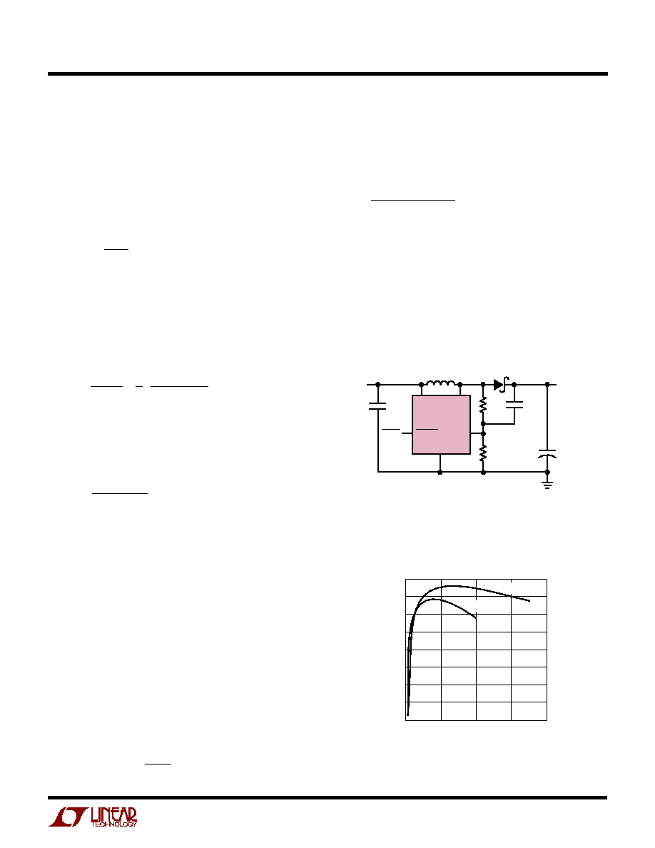
LTC1876
29
1876fa
Choosing 1% resistors; R1 = 25.5k and R2 = 32.4k yields
an output voltage of 1.816V.
The power dissipation on the top side MOSFET can be
easily estimated. Choosing a Siliconix Si4412DY results
in; R
DS(ON)
= 0.042
, C
RSS
= 100pF. At maximum input
voltage with T(estimated) = 50
∞
C:
P
V
V
C
C
V
A
pF
kHz
mW
MAIN
=
( )
+
∞
∞
[
]
(
)
+
( ) ( )( )(
)
=
1 8
22
5
1
0 005 50
25
0 042
1 7 22
5
100
300
220
2
2
.
( .
)(
≠
)
.
.
A short-circuit to ground will result in a folded back
current of:
I
mV
ns
V
H
A
SC
=
+
µ
=
25
0 01
1
2
200
22
3 3
3 2
.
(
)
.
.
with a typical value of R
DS(ON)
and
= (0.005/
∞
C)(20)
= 0.1. The resulting power dissipated in the bottom
MOSFET is:
P
V
V
V
A
mW
SYNC
=
( ) ( )
(
)
=
22
1 8
22
3 2
1 1 0 042
434
2
≠ .
.
.
.
which is less than under full-load conditions.
C
IN
is chosen for an RMS current rating of at least 3A at
temperature assuming only this channel is on. C
OUT
is
chosen with an ESR of 0.02
for low output ripple. The
output ripple in continuous mode will be highest at the
maximum input voltage. The output voltage ripple due to
ESR is approximately:
V
ORIPPLE
= R
ESR
(
I
L
) = 0.02
(1.67A) = 33mV
P≠P
Design Example for Auxiliary Regulator
Assume the requirements are V
IN
= 5V, V
OUT
= 12V and
I
OUTMAX
= 300mA. The duty cycle is given by:
Duty Cycle
V
V
IN
OUT
=
=
1
0 58
≠
.
Since the required output current is 300mA, the ripple
current of the inductor is calculated to be 0.57A.
Hence the required inductor is:
L
V
Duty Cycle
f
I
IN
L
=
(
∑
)
( ∑
)
With the boost regulator operating at 1.2MHz,
L = 4.24
µ
H
A 10
µ
H inductor is selected for the circuit for lower ripple
inductor current. Since the output current is only 300mA,
a 0.5A MBR0520 Schottky is selected. The completed
circuit along with its efficiency curve is shown in Figure 13
and Figure 14 respectively.
APPLICATIO S I FOR ATIO
W
U
U
U
Figure 13. Design Example Schematic
Figure 14. Efficiency Curve for Design Example
1876 F13
LTC1876
AUXV
IN
V
IN3
5V
V
OUT3
12V
300mA
C
IN3
2.2
µ
F
C
OUT3
4.7
µ
F
AUXSW
AUXSD AUXV
FB
SGND
+
SHDN
R8
113k
R7
13.3k
C3*
10pF
L3
10
µ
H
C1: TAIYO YUDEN X5R LMK212BJ225MG
C2: TAIYO YUDEN X5R EMK316BJ475ML
D1: ON SEMICONDUCTOR MBR0520
L1: SUMIDA CR43-100
*OPTIONAL
D1
LOAD CURRENT (mA)
0
EFFICIENCY (%)
300
400
1876 F14
100
200
90
85
80
75
70
65
60
55
50
V
IN
= 3.3V
V
IN
= 5V
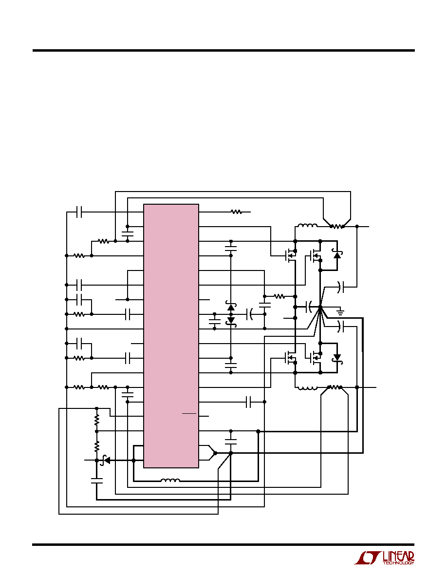
LTC1876
30
1876fa
PC Board Layout Checklist
When laying out the printed circuit board, the following
checklist should be used to ensure proper operation of the
LTC1876. These items are also illustrated graphically in
the layout diagram of Figure 15. The Figure 16 illustrates
the current waveforms present in the various branches of
the 2-phase synchronous regulators operating in the
continuous mode. Check the following in your layout:
APPLICATIO S I FOR ATIO
W
U
U
U
1. Are the top N-channel MOSFETs M1 and M3 located
within 1cm of each other with a common drain connection
at C
IN
? Do not attempt to split the input decoupling for the
two channels as it can cause a large resonant loop.
2. Is the ground of the step-down controller kept separate
from the ground of the step-up regulator? The regulator
ground should join the controller ground at the combined
C
OUT
(≠) plates. Within the controller circuitry, are the
signal and power grounds kept separate? The controller
Figure 15. LTC1876 Recommended Printed Circuit Layout Diagram
C
B1
C
B2
C
AUXIN
V
PULL-UP
(<7V)
C
INTVCC
1
2
3
4
5
6
7
8
9
10
11
12
13
14
15
16
17
18
36
35
34
33
32
31
30
29
28
27
26
25
24
23
22
21
20
19
+
C
IN
D1
M1
M2
M3
M4
D2
+
C
VIN
V
IN
R
IN
INTV
CC
3.3V
R4
R3
R7
R8
R2
R1
RUN/SS1
SENSE1
+
SENSE1
≠
V
OSENSE1
FREQSET
STBYMD
FCB
I
TH1
SGND
3.3V
OUT
I
TH2
V
OSENSE2
SENSE2
≠
SENSE2
+
AUXSGND
AUXV
FB
AUXSW
AUXSW
PGOOD
TG1
SW1
BOOST1
V
IN
BG1
EXTV
CC
INTV
CC
PGND
BG2
BOOST2
SW2
TG2
RUN/SS2
AUXSD
AUXV
IN
AUXPGND
AUXPGND
LTC1876
L1
L2
C
OUT1
V
OUT1
V
OUT2
1876 F15
+
C
OUT2
+
R
SENSE
R
SENSE
SHUTDOWN
V
OUT3
C
OUT3
D3
L3
4
3
2
1
4
3
2
1
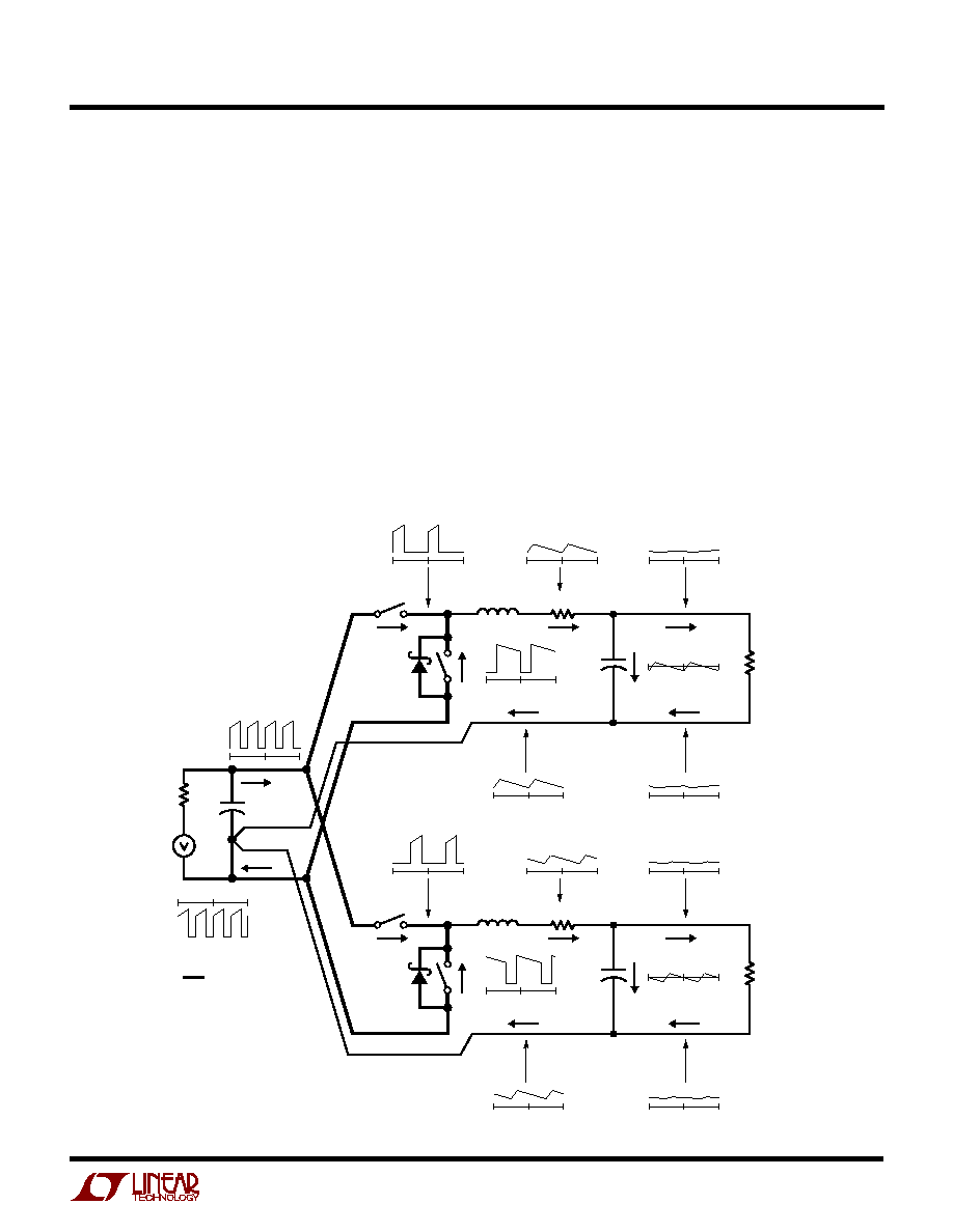
LTC1876
31
1876fa
signal ground pin and the ground return of C
INTVCC
must
return to the combined C
OUT
(≠) plates. Within the regula-
tor circuitry, are the signal and power grounds kept
separate? The regulator signal ground pin must return to
the C
AUXIN
(≠) plates.
3. Does the path formed by the top N-Channel MOSFET
Schottky diode (D1, D2) and the C
IN
capacitor have short
leads and PC trace lengths? The output capacitor (≠)
plates should be connected as close as possible to the
(≠) plates of the input capacitor by placing the capacitors
next to each other and away from the Schottky loop
described above. Also, the path formed by the AUXSW
pins, Schottky diode (D3) and the C
OUT3
capacitor should
have short leads and PC trace lengths. The C
AUXIN
capaci-
tor (≠) plates should be connected as close as possible to
Figure 16. Branch Current Waveforms
the (≠) plates of the C
OUT3
(≠) plates by placing the
capacitors next to each other and away from the D3 loop
described above.
4. If the input supply to the boost regulator is obtain from
one of the other outputs, is this connection short (< 1cm)?
5. Do the LTC1876 V
OSENSE
and AUXV
FB
pins resistive
dividers connect to the (+) plates of its respective C
OUT
?
The resistive divider must be connected between the (+)
plate of C
OUT
and signal ground and a small V
OSENSE
decoupling capacitor should be as close as possible to the
LTC1876 SGND pin. A feedforward capacitor across R8
can be connected to enhance the transient response of the
boost regulator. The R2, R4 and R8 connections should
not be along the high current input feeds from the input
capacitor(s).
APPLICATIO S I FOR ATIO
W
U
U
U
R
L1
D1
L1
SW1
R
SENSE1
V
OUT1
C
OUT1
+
V
IN
C
IN
R
IN
+
R
L2
D2
BOLD LINES INDICATE
HIGH, SWITCHING
CURRENT LINES.
KEEP LINES TO A
MINIMUM LENGTH.
L2
SW2
1876 F16
R
SENSE2
V
OUT2
C
OUT2
+

LTC1876
32
1876fa
6. Are the SENSE
≠
and SENSE
+
leads routed together with
minimum PC trace spacing? The filter capacitor between
SENSE
+
and SENSE
≠
should be as close as possible to the
IC.
7. Is the INTV
CC
decoupling capacitor connected close to
the IC, between
the INTV
CC
and the power ground pins?
This capacitor carries the MOSFET drivers current peaks.
An additional 1
µ
F ceramic capacitor placed immediately
next to the INTV
CC
and PGND pins can help improve noise
performance substantially.
8. Keep the switching nodes (SW1, SW2, AUXSW), top
gate nodes (TG1, TG2), and boost nodes (BOOST1,
BOOST2) away from sensitive small-signal nodes, espe-
cially from the opposites channel's voltage and current
sensing feedback pins. All of these nodes have very large
and fast moving signals and therefore should be kept on
the "output side" of the LTC1876 and occupy minimum PC
trace area.
9. Use a modified "star ground" technique: a low imped-
ance, large copper area central grounding point on the
same side of the PC board as the input and output
capacitors with tie-ins for the bottom of the INTV
CC
decoupling capacitor, the bottom of the voltage feedback
resistive divider and the SGND pin of the IC.
PC Board Layout Debugging
Start with one regulator on at a time. It is best to first start
with one of the step-down regulator and it is helpful to use
a DC-50MHz current probe to monitor the current in the
inductor while testing the circuit. Monitor the output
switching node (SW pin) to synchronize the oscilloscope
to the internal oscillator and probe the actual output
voltage as well. Check for proper performance over the
operating voltage and current range expected in the
application. The frequency of operation should be main-
tained over the input voltage range down to dropout and
until the output load drops below the low current operation
threshold--typically 10% to 20% of the maximum de-
signed current level in Burst Mode operation.
The duty cycle percentage should be maintained from
cycle to cycle in a well-designed, low noise PCB imple-
mentation. Variation in the duty cycle at a subharmonic
rate can suggest noise pickup at the current or voltage
sensing inputs or inadequate loop compensation. Over-
compensation of the loop can be used to tame a poor PC
layout if regulator bandwidth optimization is not required.
Only after each controller is checked for their individual
performance should both controllers be turned on at the
same time. A particularly difficult region of operation is
when one controller channel is nearing its current com-
parator trip point when the other channel is turning on its
top MOSFET. This occurs around 50% duty cycle on either
channel due to the phasing of the internal clocks and may
cause minor duty cycle jitter.
Short-circuit testing can be performed to verify proper
overcurrent latchoff, or 5
µ
A can be provided to the
RUN/SS pin(s) by resistors from V
IN
or INTV
CC
(depend-
ing upon the STBYMD pin programming), to prevent the
short-circuit latchoff from occurring.
Reduce V
IN
from its nominal level to verify operation of the
regulator in dropout. Check the operation of the undervolt-
age lockout circuit by further lowering V
IN
and monitoring
the outputs to verify operation.
Investigate whether any problems exist only at higher
output currents or only at higher input voltages. If prob-
lems coincide with high input voltages and low output
currents, look for capacitive coupling between the BOOST,
SW, TG, and possibly BG connections and the sensitive
voltage and current pins. The capacitor placed across the
current sensing pins needs to be placed immediately
adjacent to the pins of the IC. This capacitor helps to
minimize the effects of differential noise injection due to
high frequency capacitive coupling. If problems are en-
countered with high current output loading at lower input
voltages, look for inductive coupling between C
IN
, Schot-
tky and the top MOSFET components to the sensitive
current and voltage sensing traces. In addition, investigate
common ground path voltage pickup between these com-
ponents and the SGND pin of the IC.
APPLICATIO S I FOR ATIO
W
U
U
U
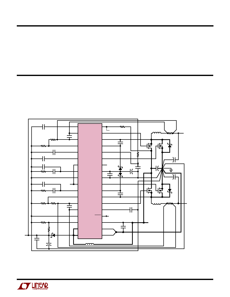
LTC1876
33
1876fa
Low Voltage 3.3V to 1.8V, 2.5V and 5V Power Supply
4.7
µ
F
1
2
3
4
5
6
7
8
9
10
11
12
13
14
15
16
17
18
36
35
34
33
32
31
30
29
28
27
26
25
24
23
22
21
20
19
+
33
µ
F
6.3V, SP
D1
M1
M2
M3
M4
D2
+
V
IN
3.3V
3.3V
OUT
RUN/SS1
SENSE1
+
SENSE1
≠
V
OSENSE1
FREQSET
STBYMD
FCB
I
TH1
SGND
3.3V
OUT
I
TH2
V
OSENSE2
SENSE2
≠
SENSE2
+
AUXSGND
AUXV
FB
AUXSW
AUXSW
PGOOD
TG1
SW1
BOOST1
V
IN
BG1
EXTV
CC
INTV
CC
PGND
BG2
BOOST2
SW2
TG2
RUN/SS2
AUXSD
AUXV
IN
AUXPGND
AUXPGND
LTC1876
L1
2
µ
H
L2
2
µ
H
47
µ
F
6.3V
SP
47
µ
F
6.3V
SP
V
OUT1
2.5V
4A
V
OUT2
1.8V
5A
1876 TA02
+
+
R
SENSE
0.008
R
SENSE
0.008
SHUTDOWN
V
OUT3
5V
400mA
10
µ
F
20V
D5
L3, 5.4
µ
H
0.1
µ
F
0.1
µ
F
1
µ
F
1
µ
F
0.1
µ
F
0.01
µ
F
0.01
µ
F
0.1
µ
F
0.1
µ
F
PGOOD
100k
D3
D4
10
+
31.6k
10k
20k
1%
20k
1%
42.5k
1%
25k
1%
6.8k
6.8k
1000pF
1000pF
470pF
220pF
220pF
470pF
M1, M2, M3, M4: FDS6912A
L1, L2: SUMIDA CEP123-2RO
L3: SUMIDA CDRH5D18
D1, D2: MBRM140T3
D3, D4: BAT54A
D5: MBR0520
10
µ
F
16V
◊
5R
4
3
2
1
4
3
2
1
An embarrassing problem, which can be missed in an
otherwise properly working switching regulator, results
when the current sensing leads are hooked up backwards.
The output voltage under this improper hookup will still be
maintained but the advantages of current mode control
will not be realized. Compensation of the voltage loop will
be much more sensitive to component selection. This
behavior can be investigated by temporarily shorting out
the current sensing resistor--don't worry, the regulator
will still maintain control of the output voltage.
APPLICATIO S I FOR ATIO
W
U
U
U
TYPICAL APPLICATIO S
U
LTC1876
34
1876fa
3.3V
IN
Dual-Phase High Efficiency Power Supply
10
µ
F
6.3V
1
µ
F
6.3V
1
2
3
4
5
6
7
8
9
10
11
12
13
14
15
16
17
18
36
35
34
33
32
31
30
29
28
27
26
25
24
23
22
21
20
19
+
D1
M1
◊
2
M2
◊
2
M3
◊
2
M4
◊
2
D2
+
3.3V
RUN/SS1
SENSE1
+
SENSE1
≠
V
OSENSE1
FREQSET
STBYMD
FCB
I
TH1
SGND
3.3V
OUT
I
TH2
V
OSENSE2
SENSE2
≠
SENSE2
+
AUXSGND
AUXV
FB
AUXSW
AUXSW
PGOOD
TG1
SW1
BOOST1
V
IN
BG1
EXTV
CC
INTV
CC
PGND
BG2
BOOST2
SW2
TG2
RUN/SS2
AUXSD
AUXV
IN
AUXPGND
AUXPGND
LTC1876
L1
0.9
µ
H
L2
0.9
µ
H
C4
1
µ
F
6.3V
C26
1
µ
F
6.3V
V
OUT1
2.5V
15A
V
OUT2
1.8V
15A
1876 TA04
+
R
SENSE
0.003
R
SENSE
0.003
SHUTDOWN
10
µ
F
10V
D3
L3, 47
µ
H
0.1
µ
F
0.47
µ
F
2.2
µ
F
6.3V
0.47
µ
F
0.01
µ
F
0.01
µ
F
100pF
V
PULL-UP
(<7V)
100k
D4
10
+
30.9k
1%
10.2k
1%
8.06k
1%
8.25k
1%
17.4k
1%
10k
1%
47k
47k
1000pF
1
µ
F
6.3V
1000pF
6800pF
100pF
100pF
6800pF
D1, D2: MBRS340T3
D3: CMDSH-3
D4: BAT54A
V
IN
3.3V
4
3
2
1
4
3
2
1
1
µ
F
6.3V
1
µ
F
6.3V
+
C
OUT1
220
µ
F, 4V,
◊
3
C
OUT2
330
µ
F, 2.5V,
◊
3
C
IN
330
µ
F
6V,
◊
3
L1, L2: SUMIDA CEP134-OR9
L3: TOKO FSLB2520-470K
M1, M2, M3, M4: FDS7764A
TYPICAL APPLICATIO S
U
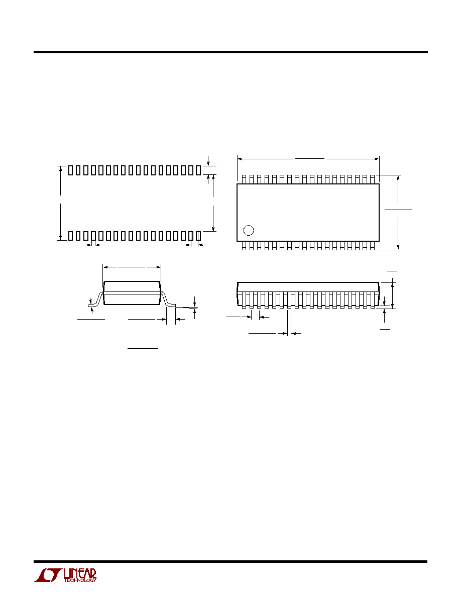
LTC1876
35
1876fa
PACKAGE DESCRIPTIO
U
Information furnished by Linear Technology Corporation is believed to be accurate and reliable.
However, no responsibility is assumed for its use. Linear Technology Corporation makes no represen-
tation that the interconnection of its circuits as described herein will not infringe on existing patent rights.
G36 SSOP 0802
0.09 ≠ 0.25
(.0035 ≠ .010)
0
∞
≠ 8
∞
0.55 ≠ 0.95
(.022 ≠ .037)
5.00 ≠ 5.60**
(.197 ≠ .221)
7.40 ≠ 8.20
(.291 ≠ .323)
1 2 3 4 5 6 7 8 9 10 11 12
14 15 16 17 18
13
12.50 ≠ 13.10*
(.492 ≠ .516)
25
26
22 21 20 19
23
24
27
28
29
30
31
32
33
34
35
36
2.0
(.079)
0.05
(.002)
0.65
(.0256)
BSC
0.22 ≠ 0.38
(.009 ≠ .015)
MILLIMETERS
(INCHES)
DIMENSIONS DO NOT INCLUDE MOLD FLASH. MOLD FLASH
SHALL NOT EXCEED .152mm (.006") PER SIDE
DIMENSIONS DO NOT INCLUDE INTERLEAD FLASH. INTERLEAD
FLASH SHALL NOT EXCEED .254mm (.010") PER SIDE
*
**
NOTE:
1. CONTROLLING DIMENSION: MILLIMETERS
2. DIMENSIONS ARE IN
3. DRAWING NOT TO SCALE
0.42
±
0.03
0.65 BSC
5.3 ≠ 5.7
7.8 ≠ 8.2
RECOMMENDED SOLDER PAD LAYOUT
1.25
±
0.12
G Package
36-Lead Plastic SSOP (5.3mm)
(Reference LTC DWG # 05-08-1640)

LTC1876
36
1876fa
PART NUMBER
DESCRIPTION
COMMENTS
LTC1625/LTC1775
No R
SENSE
TM
Current Mode Synchronous Step-Down Controllers
Burst Mode Operation, GN-16
LTC1628/LTC1628-PG High Efficiency, Dual, 2 Phase Synchronous Step-Down Controllers
Constant Frequency, Standby, 5V and 3.3V LDO
LTC1708-PG
Dual, 2 Phase Synchronous Controller with Mobile VID Control
36V Input; V
OUT1
for CPU Core Voltage;
V
OUT2
for Memory, Chipset I/O
LTC1709
2 Phase, 5-Bit Adustable, High Efficiency, Synchronous Step-Down Controller
Constant Frequency, VID, up to 42A
LTC1735
High Efficiency Synchronous Step-Down Switching Regulator
Output Fault Protection, GN-16
LTC1736
High Efficiency Synchronous Controller with Mobile VID Control
Output Fault Protection, G-24
LTC1772
SOT-23 Step-Down Controller
2.5V
V
IN
9.8V; I
OUT
Up to 4.5A; 550kHz
Operation for Smallest PCB Area
LTC1778
No R
SENSE
Wide Input Range Synchronous Step-Down Controller
Up to 97% Efficiency; 4V
V
IN
36V
0.8V
V
OUT
(0.9)(V
IN
); Input up to 20A
LTC3713
Low Input Voltage Synchronous Step-Down Controller
1.5V
V
IN
, No R
SENSE
, Standard 5V-Logic Level
MOSFETs
LTC3714
No R
SENSE
DC/DC Controller for Mobile Pentium Processors
Supports up to 25A; Sense Resistor Optional
LTC3716
2-Phase DC/DC Controller for Mobile Pentium Processors
Small, Low Profile Design; Supports up to 30A
LTC3728
Dual, 2-Phase 550kHz Synchronous Step-Down Controller
Phase-Lockable from 250kHz to 550kHz,
5mm
◊
5mm QFN and SSOP-28, 3.5V
V
IN
36V
Adaptive Power and No R
SENSE
are trademarks of Linear Technology Corporation.
Linear Technology Corporation
1630 McCarthy Blvd., Milpitas, CA 95035-7417
(408) 432-1900
q
FAX: (408) 434-0507
q
www.linear.com
©
LINEAR TECHNOLOGY CORPORATION 2000
LT/TP 1002 1K REV A ∑ PRINTED IN USA
RELATED PARTS
TYPICAL APPLICATIO
N
U
High Efficiency Triple 5V/ 3.3V/12V Power Supply
4.7
µ
F
10V
1
2
3
4
5
6
7
8
9
10
11
12
13
14
15
16
17
18
36
35
34
33
32
31
30
29
28
27
26
25
24
23
22
21
20
19
+
33
µ
F
35V
10
µ
F
35V
D1
M1
M2
M3
M4
D2
+
3.3V
RUN/SS1
SENSE1
+
SENSE1
≠
V
OSENSE1
FREQSET
STBYMD
FCB
I
TH1
SGND
3.3V
OUT
I
TH2
V
OSENSE2
SENSE2
≠
SENSE2
+
AUXSGND
AUXV
FB
AUXSW
AUXSW
PGOOD
TG1
SW1
BOOST1
V
IN
BG1
EXTV
CC
INTV
CC
PGND
BG2
BOOST2
SW2
TG2
RUN/SS2
AUXSD
AUXV
IN
AUXPGND
AUXPGND
LTC1876
L1
4.6
µ
H
L2
4.6
µ
H
47
µ
F
6.3V
SP
56
µ
F
4V
SP
V
OUT1
3.3V
5A
V
OUT2
5V
5A
1876 TA03
+
+
R
SENSE
0.008
R
SENSE
0.008
SHUTDOWN
V
OUT3
12V
200mA
10
µ
F
20V
D5
L3, 10
µ
H
0.1
µ
F
0.1
µ
F
1
µ
F
0.1
µ
F
0.01
µ
F
0.01
µ
F
0.1
µ
F
0.1
µ
F
V
PULL-UP
(<7V)
100k
D3
D4
10
+
86.6k
10.2k
20k
1%
20k
1%
63.4k
1%
105k
1%
6.8k
6.8k
1000pF
1000pF
470pF
220pF
220pF
470pF
M1, M2, M3, M4: FDS6912A
L1, L2: SUMIDA CEP123-4R6
L3: TOKO A920CY-100M
D1, D2: MBRM140T3
D3, D4: BAT54A
D5: CMDSH-3
INTV
CC
V
IN
5.2V TO 28V
4
3
2
1
4
3
2
1