19098i.pm6
1
LTC1909-8
19098f
FEATURES
APPLICATIO S
U
DESCRIPTIO
U
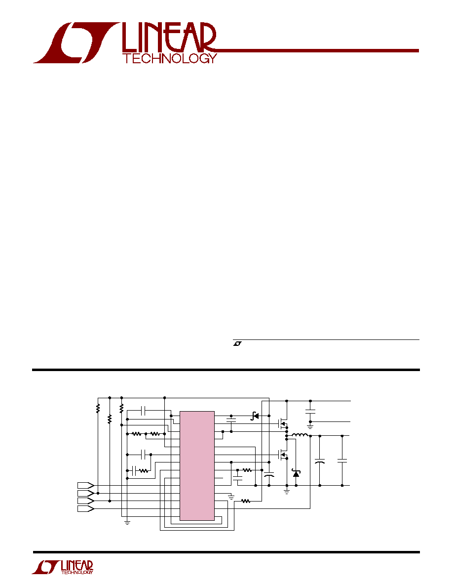
TYPICAL APPLICATIO
U
Wide Operating Range,
No R
SENSE
TM
Step-Down DC/DC
Controller with SMBus Programming
s
SMBus/I
2
C
TM
Programmable Output Voltage:
1.3V to 3.5V
s
No Sense Resistor Required
s
2% to 90% Duty Cycle at 200kHz
s
t
ON(MIN)
100ns
s
True Current Mode Control
s
Stable with Ceramic C
OUT
s
Power Good Output Voltage Monitor and 50
µ
s Timer
s
Wide V
IN
Range: 4V to 36V (Abs Max)
s
Precision Resistor Divider and Reference Provide
±
1.35% Output Voltage Accuracy Over Temperature
s
Adjustable Switching Frequency and Current Limit
s
Forced Continuous Control Pin
s
Programmable Soft-Start
s
Output Overvoltage Protection
s
Optional Short-Circuit Shutdown Timer
s
Available in a 28-Lead SSOP Package
s
Power Supplies for DSPs, ASICs, FPGAs and CPUs
s
Voltage Margining
The LTC
®
1909-8 is a synchronous step-down switching
regulator controller with a digitally programmable output
voltage. The output voltage is selected from one of two
5-bit settings programmed into internal registers via a
2-wire SMBus/I
2
C interface. The interface features safe-
guards against invalid output voltages and allows the mi-
croprocessor to turn the regulator on and off. Valley cur-
rent control delivers very low duty cycles without requiring
a sense resistor. Operating frequency is selected by an
external resistor and is compensated for variations in V
IN
and V
OUT
.
Discontinuous mode operation provides high efficiency
operation at light loads. A forced continuous control pin
reduces noise and RF interference and can assist second-
ary winding regulation by disabling discontinuous mode
operation when the main output is lightly loaded.
Fault protection is provided by internal foldback current
limiting, an output overvoltage comparator and optional
short-circuit shutdown timer.
The LTC1909-8 is available in the 28-lead SSOP package.
, LTC and LT are registered trademarks of Linear Technology Corporation.
No R
SENSE
is a trademark of Linear Technology Corporation.
I
2
C is a trademark of Philips Electronics N.V.
Figure 1. High Efficiency Step-Down Converter
1
2
3
4
5
6
7
8
9
10
11
12
13
14
28
27
26
25
24
23
22
21
20
19
18
17
16
15
RUN/SS
V
ON
PGOOD
V
RNG
FCB
I
TH
SGND
I
ON
V
FB
SEL
SDA
SCL
VRON
PGTMR
BOOST
TG
SW
SENSE
+
PGND
BG
INTV
CC
V
IN
EXTV
CC
V
CC
GND
FB
V
OSENSE
CPUON
470pF
SEL
SDA
SCL
VRON
100pF
0.1
µ
F
100k
20k
39k
100k
100k
11k
1
R
ON
1.4M 1%
C
IN
: UNITED CHEMICON THCR60E1H106TZ
C
OUT1, 2
: CORNELL DUBILIER ESRE181ME04B/
PANASONIC EEFVEOG181R
D1: DIODES INC. B340A
L1: SUMIDA CEP125-1R8MC-H
M1: Si4884
M2: Si4874
0.22
µ
F
CMDSH-3
0.1
µ
F
LTC1909-8
4.7
µ
F
6.3V
M2
D1
19098 F01
+
C
OUT1, 2
180
µ
F
4V
×
2
C
OUT3
22
µ
F
6.3V
X7R
+
M1
V
IN
5V TO 24V
V
OUT
2.5V OR 2.6V
10A
(V
OUT
SET BY SEL)
GND
GND
C
IN
10
µ
F
50V
×
4
L1
1.8
µ
H
5V
EXT
2
LTC1909-8
19098f
(Note 1)
Input Supply Voltage
V
IN
, I
ON
.................................................. 0.3V to 36V
Boosted Topside Driver Supply Voltage
BOOST .................................................. 0.3V to 42V
SW, SENSE
+
Voltages ................................. 5V to 36V
EXTV
CC
, (BOOST SW), RUN/SS, PGOOD, INTV
CC
,
SEL, SDA, SCL, VRON, PGTMR, V
OSENSE
,
FB, CPUON, V
CC
Voltages .......................... 0.3V to 7V
FCB, V
ON
, V
RNG
Voltages ....... 0.3V to (INTV
CC
+ 0.3V)
I
TH
, V
FB
Voltages...................................... 0.3V to 2.7V
TG, BG, INTV
CC
, EXTV
CC
Peak Currents .................... 2A
TG, BG, INTV
CC
, EXTV
CC
RMS Currents .............. 50mA
Operating Ambient Temperature Range
LTC1909-8EG (Note 2) ....................... 40
°
C to 85
°
C
Junction Temperature (Note 4) ............................ 125
°
C
Storage Temperature Range ................. 65
°
C to 150
°
C
Lead Temperature (Soldering, 10 sec).................. 300
°
C
ORDER PART
NUMBER
LTC1909-8EG
T
JMAX
= 125
°
C,
JA
= 95
°
C/ W
(Switching Regulator Controller) The
q
denotes specifications which apply
over the full operating temperature range, otherwise specifications are T
A
= 25
°
C. V
IN
= 15V unless otherwise noted.
ABSOLUTE AXI U RATI GS
W
W
W
U
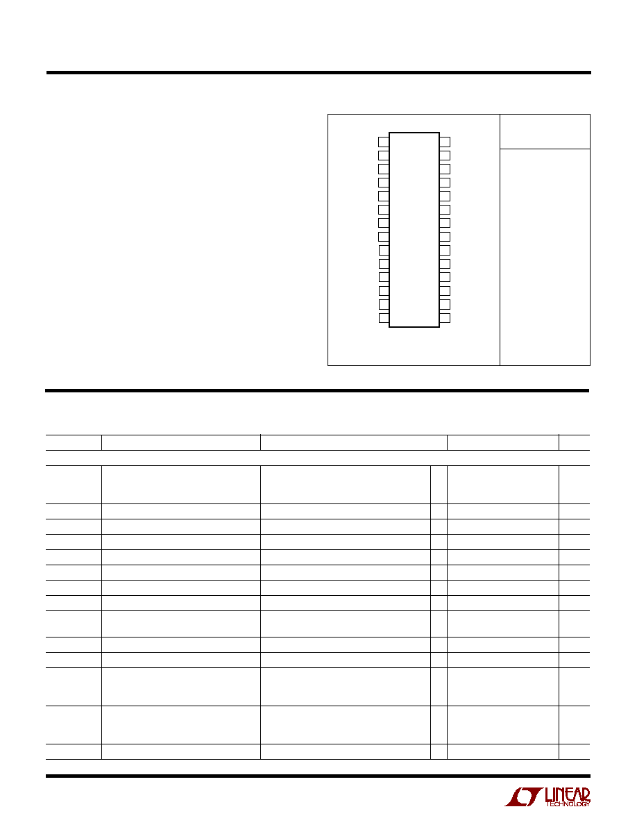
PACKAGE/ORDER I FOR ATIO
U
U
W
ELECTRICAL CHARACTERISTICS
1
2
3
4
5
6
7
8
9
10
11
12
13
14
TOP VIEW
G PACKAGE
28-LEAD PLASTIC SSOP
28
27
26
25
24
23
22
21
20
19
18
17
16
15
RUN/SS
V
ON
PGOOD
V
RNG
FCB
I
TH
SGND
I
ON
V
FB
SEL
SDA
SCL
VRON
PGTMR
BOOST
TG
SW
SENSE
+
PGND
BG
INTV
CC
V
IN
EXTV
CC
V
CC
GND
FB
V
OSENSE
CPUON
Consult LTC Marketing for parts specified with wider operating temperature ranges.
SYMBOL
PARAMETER
CONDITIONS
MIN
TYP
MAX
UNITS
Main Control Loop
I
Q
Input DC Supply Current
Normal
900
2000
µ
A
Shutdown Supply Current
15
30
µ
A
V
FB
Feedback Reference Voltage
I
TH
= 1.2V (Note 3)
q
0.792
0.800
0.808
V
V
FB(LINEREG)
Feedback Voltage Line Regulation
V
IN
= 4V to 30V, I
TH
= 1.2V (Note 3)
0.002
%/V
V
FB(LOADREG)
Feedback Voltage Load Regulation
I
TH
= 0.5V to 1.9V (Note 3)
q
0.05
0.3
%
I
FB
Feedback Input Current
V
FB
= 0.8V
5
±
50
nA
g
m(EA)
Error Amplifier Transconductance
I
TH
= 1.2V (Note 3)
q
1.4
1.7
2
mS
V
FCB
Forced Continuous Threshold
q
0.76
0.8
0.84
V
I
FCB
Forced Continuous Pin Current
V
FCB
= 0.8V
1
2
µ
A
t
ON
On-Time
I
ON
= 60
µ
A, V
ON
= 1.5V
212
250
288
ns
I
ON
= 30
µ
A, V
ON
= 1.5V
425
500
575
ns
t
ON(MIN)
Minimum On-Time
I
ON
= 180
µ
A, V
ON
= 0V
50
100
ns
t
OFF(MIN)
Minimum Off-Time
I
ON
= 60
µ
A, V
ON
= 1.5V
250
400
ns
V
SENSE(MAX)
Maximum Current Sense Threshold
V
RNG
= 1V, V
FB
= 0.76V
113
133
153
mV
V
PGND
V
SENSE
+
V
RNG
= 0V, V
FB
= 0.76V
q
79
93
107
mV
V
RNG
= INTV
CC
, V
FB
= 0.76V
158
186
214
mV
V
SENSE(MIN)
Minimum Current Sense Threshold
V
RNG
= 1V, V
FB
= 0.84V
67
mV
V
PGND
V
SENSE
+
V
RNG
= 0V, V
FB
= 0.84V
47
mV
V
RNG
= INTV
CC
, V
FB
= 0.84V
93
mV
V
FB(OV)
Output Overvoltage Fault Threshold
5.5
7.5
9.5
%
3
LTC1909-8
19098f
(Switching Regulator Controller) The
q
denotes specifications which apply
over the full operating temperature range, otherwise specifications are T
A
= 25
°
C. V
IN
= 15V unless otherwise noted.
ELECTRICAL CHARACTERISTICS
(SMBus VID Programmer) The
q
denotes the specifications which apply over the full operating temperature range, otherwise
specifications are at T
A
= 25
°
C. 2.7V
V
CC
5.5V (Note 5) unless otherwise stated.
SYMBOL
PARAMETER
CONDITIONS
MIN
TYP
MAX
UNITS
V
CC
Operating Supply Voltage Range
2.7
5.5
V
I
CC
Supply Current
CPUON, PGTMR Pins Are Open
q
350
µ
A
R
FB-SENSE
Resistance Between V
OSENSE
and FB
q
14
20
26
k
DE
Divider Error (Note 6)
V
OSENSE
Programmed from 1.3V to 3.5V
q
0.35
0.35
%
V
IH
SCL, SDA Input High Voltage
q
2.1
V
V
IL
SCL, SDA Input Low Voltage
q
0.8
V
V
IH
SEL, VRON Input High Voltage
1.3
2
V
V
IL
SEL, VRON Input Low Voltage
q
0.8
1.3
V
V
HYST
SEL, VRON Hysteresis
±
50
mV
V
OL
SDA, CPUON PGTMR Output Low Voltage I = 3mA
q
0.4
V
I
IN
SCL, SDA, SEL, VRON Input Current
SDA Not Acknowledging, 0
V
PIN
5.5V,
q
±
10
µ
A
V
PIN
= 5.5V for VRON only
SYMBOL
PARAMETER
CONDITIONS
MIN
TYP
MAX
UNITS
V
FB(UV)
Output Undervoltage Fault Threshold
520
600
680
mV
V
RUN/SS(ON)
RUN Pin Start Threshold
q
0.8
1.5
2
V
V
RUN/SS(LE)
RUN Pin Latchoff Enable Threshold
RUN/SS Pin Rising
4
4.5
V
V
RUN/SS(LT)
RUN Pin Latchoff Threshold
RUN/SS Pin Falling
3.5
4.2
V
I
RUN/SS(C)
Soft-Start Charge Current
V
RUN/SS
= 0V
0.5
1.2
3
µ
A
I
RUN/SS(D)
Soft-Start Discharge Current
V
RUN/SS
= 4.5V, V
FB
= 0V
0.8
1.8
3
µ
A
V
IN(UVLO)
Undervoltage Lockout
V
IN
Falling
q
3.4
3.9
V
V
IN(UVLOR)
Undervoltage Lockout Release
V
IN
Rising
q
3.5
4
V
TG R
UP
TG Driver Pull-Up On Resistance
TG High
2
3
TG R
DOWN
TG Driver Pull-Down On Resistance
TG Low
2
3
BG R
UP
BG Driver Pull-Up On Resistance
BG High
3
4
BG R
DOWN
BG Driver Pull-Down On Resistance
BG Low
1
2
TG t
r
TG Rise Time
C
LOAD
= 3300pF, 20% to 80% of Swing
20
ns
TG t
f
TG Fall Time
C
LOAD
= 3300pF, 20% to 80% of Swing
20
ns
BG t
r
BG Rise Time
C
LOAD
= 3300pF, 20% to 80% of Swing
20
ns
BG t
f
BG Fall Time
C
LOAD
= 3300pF, 20% to 80% of Swing
20
ns
Internal V
CC
Regulator
V
INTVCC
Internal V
CC
Voltage
6V < V
IN
< 30V, V
EXTVCC
= 4V
q
4.7
5
5.3
V
V
LDO(LOADREG)
Internal V
CC
Load Regulation
I
CC
= 0mA to 20mA, V
EXTVCC
= 4V
0.1
±
2
%
V
EXTVCC
EXTV
CC
Switchover Voltage
I
CC
= 20mA, V
EXTVCC
Rising
q
4.5
4.7
V
V
EXTVCC
EXTV
CC
Switch Drop Voltage
I
CC
= 20mA, V
EXTVCC
= 5V
150
300
mV
V
EXTVCC(HYS)
EXTV
CC
Switchover Hysteresis
200
mV
PGOOD Output
V
FBH
PGOOD Upper Threshold
V
FB
Rising
5.5
7.5
9.5
%
V
FBL
PGOOD Lower Threshold
V
FB
Falling
5.5
7.5
9.5
%
V
FB(HYS)
PGOOD Hysteresis
V
FB
Returning
1
2
%
V
PGL
PGOOD Low Voltage
I
PGOOD
= 5mA
0.15
0.4
V
4
LTC1909-8
19098f
(SMBus VID Programmer) The
q
denotes the specifications which apply over the full operating temperature range, otherwise
specifications are at T
A
= 25
°
C. 2.7V
V
CC
5.5V (Note 5) unless otherwise stated.
ELECTRICAL CHARACTERISTICS
Note 1: Absolute Maximum Ratings are those values beyond which the life
of a device may be impaired.
Note 2: The LTC1909-8E is guaranteed to meet performance specifications
from 0
°
C to 70
°
C. Specifications over the 40
°
C to 85
°
C operating
temperature range are assured by design, characterization and correlation
with statistical process controls.
Note 3: The LTC1909-8 is tested in a feedback loop that adjusts V
FB
to
achieve a specified error amplifier output voltage (I
TH
).
Note 4: T
J
is calculated from the ambient temperature T
A
and power
dissipation P
D
as follows:
LTC1909-8E: T
J
= T
A
+ (P
D
· 130
°
C/W)
Note 5: All currents into device pins are positive; all currents out of device pins
are negative. All voltages are referenced to device ground unless otherwise
noted.
Note 6: The divider error is tested in a feedback loop that adjusts FB to
0.8V for each 5-bit code.
Note 7: These parameters are guaranteed by design and are not tested in
production. SMBus timing is referenced to V
IL
and V
IH
levels.
Note 8: Dominated by the switching regulator. The delay due to the SMBus
VID programmer is only 500ns typ.
Note 9: Measured from the rising edge of SDA during Data High
acknowledgment.
SYMBOL
PARAMETER
CONDITIONS
MIN
TYP
MAX
UNITS
I
SK1
SDA, PGTMR, CPUON
0
V
PIN
2.7V
q
5
19
60
mA
Sink Current at V
CC
= 2.7V
I
SK2
SDA, PGTMR, CPUON
0
V
PIN
5.5V
q
35
65
150
mA
Sink Current at V
CC
= 5.5V
I
LKG
PGTMR, CPUON Leakage Current
0
V
PIN
5.5V
±
0.2
µ
A
I
PU
VRON Pull-Up Current
V
PIN
= 0
q
1
2.5
7
µ
A
Timing (Note 7)
f
SMB
SMBus Operating Frequency
q
10
100
KHz
t
BUF
Bus Free Time Between Stop/Start
q
4.7
µ
s
t
HD:STA
Hold Time After (Repeated) Start
q
4
µ
s
t
SU:STA
Repeated Start Setup Time
q
4.7
µ
s
t
SU:STO
Stop Condition Setup Time
q
4
µ
s
t
HD:DAT
Data Hold Time
q
300
ns
t
SU:DAT
Data Setup Time
q
250
ns
t
LOW
Clock Low Period
q
4.7
µ
s
t
HIGH
Clock High Period
q
4
µ
s
t
f
SCL, SDA Fall Time
0.9V
CC
to 0.65V
q
300
ns
t
r
SCL, SDA Rise Time
0.65V to 2.25V
q
1000
ns
t
SSH
SEL to V
OSENSE
High (Note 8)
Toggle SEL to Switch from 01111B to 10000B,
q
500
ns
V
FB
= 0.8V
t
SSL
SEL to V
OSENSE
Low (Note 8)
Toggle SEL to Switch from 10000B to 01111B,
q
500
ns
V
FB
= 0.8V
t
SPL
SEL Toggling to PGTMR Low
Toggle SEL to Select New Code
q
160
500
ns
C
L
= 100pF, 10k
Pull-Up, S2 in Test Circuit
t
PH
Stop Bit to CPUON High (Note 9)
C
L
= 100pF, 10k
Pull-Up, S2 in Test Circuit
q
2
µ
s
t
PL
Stop Bit to CPUON Low (Note 9)
C
L
= 0.1
µ
F, 10k
Pull-Up, S1 in Test Circuit
q
20
50
µ
s
t
PPL
Stop Bit to PGTMR Low (Note 9)
C
L
= 100pF, 10k
Pull-Up, S2 in Test Circuit
q
250
ns
t
VH
VRON High to CPUON High
C
L
= 100pF, 10k
Pull-Up, S2 in Test Circuit
q
2
µ
s
t
VL
VRON Low to CPUON Low
C
L
= 0.1
µ
F, 10k
Pull-Up, S1 in Test Circuit
q
50
µ
s
t
VPL
VRON Low to PGTMR Low
C
L
= 100pF, 10k
Pull-Up, S2 in Test Circuit
q
130
500
ns
t
PGL
PGTMR Low Duration
C
L
= 100pF, 10k
Pull-Up, S2 in Test Circuit
30
50
70
µ
s
5
LTC1909-8
19098f
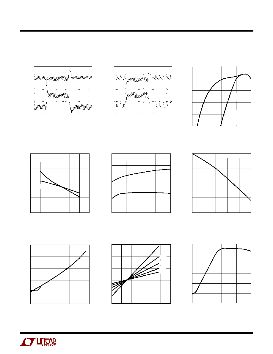
TYPICAL PERFOR A CE CHARACTERISTICS
U
W
LOAD CURRENT (A)
0.001
EFFICIENCY (%)
70
80
10
19098 G18
60
50
0.01
0.1
1
100
90
DISCONTINUOUS
MODE
CONTINUOUS
MODE
V
IN
= 10V
V
OUT
= 2.5V
EXTV
CC
= 5V
FIGURE 1 CIRCUIT
Efficiency vs Load Current
Efficiency vs Input Voltage
INPUT VOLTAGE (V)
0
80
EFFICIENCY (%)
85
90
95
100
5
10
15
20
19098 G19
25
30
I
LOAD
= 1A
I
LOAD
= 10A
FCB = 5V
FIGURE 1 CIRCUIT
Frequency vs Input Voltage
INPUT VOLTAGE (V)
5
FREQUENCY (kHz)
240
260
25
19098 G20
220
200
10
15
20
300
280
I
OUT
= 10A
FCB = 0V
FIGURE 1 CIRCUIT
I
OUT
= 0A
Load Regulation
LOAD CURRENT (A)
0
V
OUT
(%)
0.2
0.1
8
19098 G21
0.3
0.4
2
4
6
10
0
FIGURE 1 CIRCUIT
I
TH
Voltage vs Load Current
LOAD CURRENT (A)
0
I
TH
VOLTAGE (V)
1.0
1.5
19098 G22
0.5
0
5
10
15
2.5
2.0
CONTINUOUS
MODE
DISCONTINUOUS
MODE
FIGURE 1 CIRCUIT
Current Sense Threshold
vs I
TH
Voltage
I
TH
VOLTAGE (V)
0
200
CURRENT SENSE THRESHOLD (mV)
100
0
100
200
300
0.5
1.0
1.5
2.0
19098 G23
2.5
3.0
1V
0.7V
0.5V
1.4V
V
RNG
= 2V
Current Limit Foldback
V
FB
(V)
0
0
MAXIMUM CURRENT SENSE THRESHOLD (mV)
25
50
75
100
125
150
0.2
0.4
0.6
0.8
1778 G09
Transient Response
(Discontinuous Mode)
Transient Response
V
OUT
50mV/DIV
I
L
5A/DIV
20
µ
s
19098 G16
LOAD STEP 0A TO 10A
V
IN
= 15V
V
OUT
= 2.5V
FCB = 0V
FIGURE 1 CIRCUIT
V
OUT
50mV/DIV
I
L
5A/DIV
20
µ
s
19098 G17
LOAD STEP 1A TO 10A
V
IN
= 15V
V
OUT
= 2.5V
FCB = INTV
CC
FIGURE 1 CIRCUIT