1
LTC1911-1.5/LTC1911-1.8
1911f
APPLICATIO S
U
FEATURES
DESCRIPTIO
U
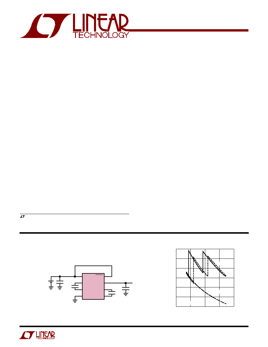
TYPICAL APPLICATIO
U
Low Noise, High Efficiency,
Inductorless Step-Down
DC/DC Converter
The LTC
Æ
1911 is a switched capacitor step-down DC/DC
converter that produces a 1.5V or 1.8V regulated output
from a 2.7V to 5.5V input. The part uses switched capaci-
tor fractional conversion to achieve high efficiency over the
entire input range. No inductors are required. Internal cir-
cuitry controls the step-down conversion ratio to optimize
efficiency as the input voltage and load conditions vary.*
Typical efficiency is over 25% higher than that of a linear
regulator.
A unique constant frequency architecture provides a low
noise regulated output as well as lower input noise than
conventional charge pump regulators. High frequency
operation (f
OSC
= 1.5MHz) simplifies output filtering to
further reduce conducted noise. To optimize efficiency,
the part enters Burst Mode
Æ
operation under light load
conditions.
Low operating current (180
µ
A with no load, 10
µ
A in
shutdown) and low external parts count (two 1
µ
F flying
capacitors and two 10
µ
F bypass capacitors) make the
LTC1911 ideally suited for space constrained battery-
powered applications. The part is short-circuit and
overtemperature protected, and is available in an 8-pin
MSOP package.
s
Low Noise Constant Frequency Operation
s
2.7V to 5.5V Input Voltage Range
s
No Inductors
s
Typical Efficiency 25% Higher Than LDOs
s
Shutdown Disconnects Load from V
IN
s
Output Voltage: 1.8V
±
4% or 1.5V
±
4%
s
Output Current: 250mA
s
Low Operating Current: I
IN
= 180
µ
A Typ
s
Low Shutdown Current: I
IN
= 10
µ
A Typ
s
Oscillator Frequency: 1.5MHz
s
Soft-Start Limits Inrush Current at Turn On
s
Short-Circuit and Overtemperature Protected
s
Available in an 8-Pin MSOP Package
, LTC and LT are registered trademarks of Linear Technology Corporation.
s
Handheld Computers
s
Cellular Phones
s
Smart Card Readers
s
Portable Electronic Equipment
s
Handheld Medical Instruments
s
Low Power DSP Supplies
V
IN
C2
+
C2
≠
GND
8
6
7
5
1
2
3
4
SS/SHDN
V
OUT
C1
+
C1
≠
LTC1911-1.8
1
µ
F*
1-CELL Li-Ion
OR
3-CELL NiMH
10
µ
F*
*CERAMIC CAPACITOR
10
µ
F*
1911 TA01
V
OUT
= 1.8V
I
OUT
= 250mA
1
µ
F*
2.7V TO 5.5V INPUT
Single Cell Li-Ion to 1.8V DC/DC Converter
Efficiency
Burst Mode is a registered trademark of Linear Technology Corporation.
*U.S. Patent #6,438,005
INPUT VOLTAGE (V)
2
30
EFFICIENCY (%)
40
50
60
70
80
90
3
4
5
6
1911 G05
IDEAL LDO
250mA
100mA
V
OUT
= 1.8V
2
LTC1911-1.5/LTC1911-1.8
1911f
PARAMETER
CONDITIONS
MIN
TYP
MAX
UNITS
V
IN
Operating Voltage
q
2.7
5.5
V
V
OUT
LTC1911-1.5, 0mA
I
OUT
250mA, V
IN
= 2.7V to 5.5V
q
1.44
1.5
1.56
V
LTC1911-1.8, 0mA
I
OUT
250mA, V
IN
= 2.7V to 5.5V
q
1.73
1.8
1.87
V
V
IN
Operating Current
I
OUT
= 0mA, V
IN
= 2.7V to 5.5V
q
180
350
µ
A
V
IN
Shutdown Current
SS/SHDN = 0V, V
IN
= 2.7V to 5.5V
q
10
20
µ
A
Output Ripple
I
OUT
= 10mA
5
mV
P-P
I
OUT
= 250mA
12
mV
P-P
V
OUT
Short-Circuit Current
V
OUT
= 0V
600
mA
Switching Frequency
Oscillator Free Running
1.2
1.5
1.8
MHz
SS/SHDN Input Threshold
q
0.3
0.6
1
V
SS/SHDN Soft-Start Current
V
SS/SHDN
= 0V (Note 3)
q
≠ 5
≠ 2
≠1
µ
A
V
SS/SHDN
= V
IN
0.01
µ
A
Turn-On Time
C
SS
= 0pF, V
IN
= 3.3V
0.03
ms
C
SS
= 10nF, V
IN
= 3.3V
10
ms
Load Regulation
0V
I
OUT
250mA
0.13
mV/mA
Line Regulation
0V
I
OUT
250mA
0.3
%/V
(Note 1)
V
IN
to GND ...................................................≠ 0.3V to 6V
SS/SHDN to GND ........................ ≠ 0.3V to (V
IN
+ 0.3V)
V
OUT
Short-Circuit Duration ............................ Indefinite
Operating Temperature Range (Note 2) .. ≠ 40
∞
C to 85
∞
C
Storage Temperature Range ................. ≠ 40
∞
C to 150
∞
C
Lead Temperature (Soldering, 10 sec).................. 300
∞
C
ORDER PART
NUMBER
LTC1911EMS8-1.5
LTC1911EMS8-1.8
T
JMAX
= 125
∞
C,
JA
= 160
∞
C/ W
The
q
denotes specifications which apply over the full operating
temperature range, otherwise specifications are T
A
= 25
∞
C. V
IN
= 3.6V, C1 = 1
µ
F, C2 = 1
µ
F, C
IN
= 10
µ
F, C
OUT
= 10
µ
F unless
otherwise noted.
ABSOLUTE AXI U RATI GS
W
W
W
U
PACKAGE/ORDER I FOR ATIO
U
U
W
MS8 PART MARKING
1
2
3
4
V
IN
C2
+
C2
≠
GND
8
7
6
5
SS/SHDN
C1
+
V
OUT
C1
≠
TOP VIEW
MS8 PACKAGE
8-LEAD PLASTIC MSOP
LTMY
LTNU
ELECTRICAL CHARACTERISTICS
Note 1: Absolute Maximum Ratings are those values beyond which the life
of a device may be impaired.
Note 2: The LTC1911E is guaranteed to meet specified performance from
0
∞
C to 70
∞
C. Specifications over the ≠ 40
∞
C to 85
∞
C operating temperature
range are assured by design, characterization and correlation with
statistical process controls.
Note 3: Currents flowing into the device are positive polarity. Currents
flowing out of the device are negative polarity.
Consult LTC Marketing for parts specified with wider operating temperature ranges.
3
LTC1911-1.5/LTC1911-1.8
1911f
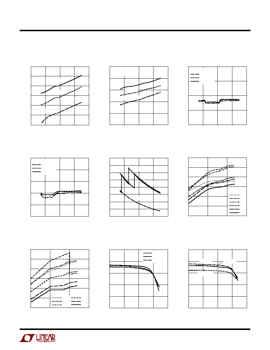
TYPICAL PERFOR A CE CHARACTERISTICS
U
W
Input Operating Current
vs Input Voltage
Input Shutdown Current
vs Input Voltage
LTC1911-1.8
Output Voltage vs Input Voltage
LTC1911-1.5
Output Voltage vs Input Voltage
LTC1911-1.5 Efficiency vs Input
Voltage (Falling Input Voltage)
LTC1911-1.8
Efficiency vs Output Current
LTC1911-1.8
Output Voltage vs Output Current
INPUT VOLTAGE (V)
2
INPUT CURRENT (
µ
A)
180
190
200
6
1911 G01
170
160
3
4
5
150
210
T
A
= 85
∞
C
T
A
= 25
∞
C
T
A
= ≠40
∞
C
INPUT VOLTAGE (V)
2
INPUT CURRENT (
µ
A)
9
11
6
1911 G02
7
5
3
4
5
15
13
T
A
= 85
∞
C
T
A
= 25
∞
C
T
A
= ≠40
∞
C
V
OUT
= 0V
V
(SS/SHDN)
= 0V
INPUT VOLTAGE (V)
2
OUTPUT VOLTAGE (V)
1.80
1.85
6
1911 G03
1.75
1.70
3
4
5
1.90
T
A
= ≠40
∞
C
T
A
= 25
∞
C
T
A
= 85
∞
C
I
OUT
= 250mA
INPUT VOLTAGE (V)
2
EFFICIENCY (%)
60
70
80
6
1911 G05
50
40
20
3
4
5
30
100
90
IDEAL LDO
100mA
250mA
OUTPUT CURRENT (mA)
1
EFFICIENCY (%)
50
60
1911 G06
40
30
10
100
1000
90
80
70
2.7V
3.2V
3.7V
4.2V
5.1V
5.5V
V
IN
:
LTC1911-1.5
Efficiency vs Output Current
OUTPUT CURRENT (mA)
0.1
OUTPUT VOLTAGE (V)
1.78
1.80
1000
1911 G08
1.76
1.74
1
10
100
1.84
V
IN
= 3.6V
1.82
T
A
= ≠40
∞
C
T
A
= 25
∞
C
T
A
= 85
∞
C
LTC1911-1.5
Output Voltage vs Output Current
INPUT VOLTAGE (V)
2
OUTPUT VOLTAGE (V)
1.49
1.51
6
LTXXXX ∑ TPCXX
1.47
1.45
3
4
5
1.55
1.53
T
A
= ≠40
∞
C
T
A
= 25
∞
C
T
A
= 85
∞
C
I
OUT
= 250mA
OUTPUT CURRENT (mA)
1
30
EFFICIENCY (%)
40
50
60
70
90
10
100
1911 G07
1000
80
2.8V
3.3V
3.7V
4.3V
5.1V
5.5V
V
IN
:
OUTPUT CURRENT (mA)
0.1
OUTPUT VOLTAGE (V)
1.48
1.50
1000
1911 G09
1.46
1.44
1
10
100
1.54
1.52
T
A
= ≠40
∞
C
T
A
= 85
∞
C
T
A
= 25
∞
C
V
IN
= 3.6V
4
LTC1911-1.5/LTC1911-1.8
1911f
TYPICAL PERFOR A CE CHARACTERISTICS
U
W
Start-Up Time
vs Soft-Start Capacitor
Output Ripple
vs Output Load Current
Output Current Transient Response
Line Transient Response
SOFT-START CAPACITOR (nF)
0.1
0.1
START-UP TIME (ms)
1
10
100
1
10
1911 G10
100
T
A
= ≠40
∞
C
T
A
= 25
∞
C
T
A
= 85
∞
C
V
IN
= 3.6V
4V
3V
V
IN
500mV/DIV
V
OUT
20mV/DIV
I
OUT
= 225mA
20
µ
s/DIV
1911 G14
250mA
25mA
I
OUT
V
OUT
20mV/DIV
V
IN
= 3.6V
10
µ
s/DIV
1911 G13
V
IN
(Pin 1): Input Supply Voltage. V
IN
may be between
2.7V and 5.5V. Suggested bypass for V
IN
is a 10
µ
F (1
µ
F
min) ceramic low ESR capacitor.
C2
+
(Pin 2): Flying Capacitor Two Positive Terminal.
C2
≠
(Pin 3): Flying Capacitor Two Negative Terminal.
GND (Pin 4): Ground. Connect to a ground plane for best
performance.
C1
≠
(Pin 5): Flying Capacitor One Negative Terminal.
V
OUT
(Pin 6): Regulated Output Voltage. V
OUT
is discon-
nected from V
IN
during shutdown. Bypass V
OUT
with a
10
µ
F ceramic low ESR capacitor (4
µ
F min, ESR < 0.1
max).
C1
+
(Pin 7): Flying Capacitor One Positive Terminal.
U
U
U
PI FU CTIO S
SS/SHDN (Pin 8): Soft-Start/Shutdown Control Pin. This
pin is designed to be driven with an external open-drain
output. Holding the SS/SHDN pin below 0.3V will force
the LTC1911-X into shutdown mode. An internal pull-up
current of 2
µ
A will force the SS/SHDN voltage to climb to
V
IN
once the device driving the pin is forced into a Hi-Z
state. To limit inrush current on start-up, connect a
capacitor between the SS/SHDN pin and GND. Capaci-
tance on the SS/SHDN pin will limit the dV/dt of the pin
during turn on which, in turn, will limit the dV/dt of V
OUT
.
By selecting an appropriate soft-start capacitor, the user
can control the inrush current for a known output capaci-
tor during turn-on (see Application Information). If nei-
ther of the two functions are desired, the pin may be left
floating or tied to V
IN
.
LTC1911-1.8 Output Voltage Ripple
V
OUT
50mV/DIV
2-TO-1 MODE
V
IN
= 5V
I
OUT
= 250mA
100ns/DIV
1911 G12
ALL WAVEFORMS AC COUPLED
OUTPUT LOAD CURRENT (mA)
0
0
OUTPUT RIPPLE (mV
P-P
)
5
10
15
20
30
50
100
150
200
1911 G11
250
300
25
C
OUT
= 4.7
µ
F
C
OUT
= 10
µ
F
C
OUT
= 22
µ
F
V
OUT
50mV/DIV
3-TO-2 MODE
V
IN
= 3.6V
V
OUT
50mV/DIV
1-TO-1 MODE
V
IN
= 2.7V
V
IN
(V)
2.5
1.40
FREQUENCY (MHz)
1.45
1.50
1.55
1.60
3.0
3.5
4.0
4.5
1911 G15
5.0
5.5
T
A
= ≠40
∞
C
T
A
= 25
∞
C
T
A
= 85
∞
C
Oscillator Frequency
vs Input Supply Voltage
5
LTC1911-1.5/LTC1911-1.8
1911f
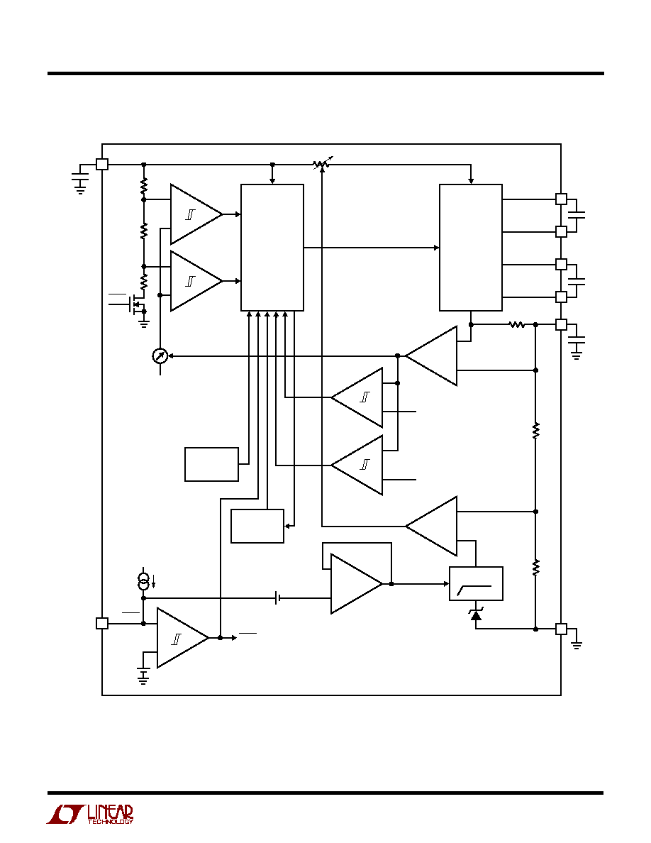
SI PLIFIED
W
BLOCK DIAGRA
W
≠
+
≠
+
300k
C
IN
V
IN
50k
150k
V
REF
+
≠
ADJ
OFFSET
MODE
CONTROL
STEP-DOWN
CHARGE
PUMP
1
R
A
≠
+
≠
+
AMP1
≠
+
≠
+
≠
+
AMP2
SOFT-START
1.26V
V
REF
COMP1
BURST
THRESHOLD
C1
+
C1
C2
C1
≠
C2
+
C2
≠
R
SENSE
V
OUT
C
OUT
6
GND
1911 BD
4
3
2
5
7
≠
+
COMP2
600mV
600mV
SHDN
SHORT-CIRCUIT
THRESHOLD
OVERTEMP
DETECT
1.5MHz
OSCILLATOR
60k
140k
V
REF
RAMP
+
2
µ
A
SS/SHDN
V
IN
8
+
SHDN
6
LTC1911-1.5/LTC1911-1.8
1911f
APPLICATIO S I FOR ATIO
W
U
U
U
General Operation
The LTC1911 uses a switch capacitor-based DC/DC con-
version to provide the efficiency advantages associated
with inductor-based circuits as well as the cost and
simplicity advantages of a linear regulator. The LTC1911's
unique constant frequency architecture provides a low
noise regulated output as well as lower input noise than
conventional switch-capacitor charge pump regulators.
The LTC1911 uses an internal switch network and frac-
tional conversion ratios to achieve high efficiency over
widely varying V
IN
and output load conditions. Internal
control circuitry selects the appropriate step-down con-
version ratio based on V
IN
and load conditions to optimize
efficiency. The part has three possible step-down modes:
2-to-1, 3-to-2 or 1-to-1 step-down mode. Only two exter-
nal flying caps are needed to operate in all three modes.
2-to-1 mode is chosen when V
IN
is greater than two times
the desired V
OUT
. 3-to-2 mode is chosen when V
IN
is
greater than 1.5 times V
OUT
but less than 2 times V
OUT
. 1-
to-1 mode is chosen when V
IN
falls below 1.5 times V
OUT
.
An internal load current sense circuit controls the switch
point of the step-down ratio as needed to maintain output
regulation over all load conditions.
Regulation is achieved by sensing the output voltage and
regulating the amount of charge transferred per cycle.
This method of regulation provides much lower input and
output ripple than that of conventional switched capacitor
charge pumps. The constant frequency charge transfer
also makes additional output or input filtering much less
demanding than conventional switched capacitor charge
pumps.
The LTC1911 also has a Burst Mode function that delivers
a minimum amount of charge for one cycle then goes into
a low current state until the output drops enough to require
another burst of charge. Burst Mode operation allows the
LTC1911 to achieve high efficiency even at light loads. The
part has shutdown capability as well as user-controlled
inrush current limiting. In addition, the part has short-
circuit and overtemperature protection.
Step-Down Charge Transfer Operation
Figure 1a shows the switch configuration that is used for
2-to-1 step down mode. In this mode, a 2-phase clock
generates the switch control signals. On phase one of the
clock, the top plate of C1 is connected to V
IN
through R
A
and S4, the bottom plate is connected to V
OUT
through S3.
The amount of charge transferred to C1 (and V
OUT
) is set
by the value of R
A
.
On phase two, flying capacitor C1 is connected to V
OUT
through S1 and to GND through S2. The charge that was
transferred onto C1 from the previous cycle is now trans-
ferred to the output. Thus, in 2-to-1 mode, charge is
transferred to V
OUT
on both phases of the clock. Since
charge current is sourced from GND on the second phase
of the clock, current multiplication is realized with respect
to V
IN
, i.e., I
OUT
equals approximately 2 ∑ I
IN
. This results
in significant efficiency improvement relative to a linear
regulator. The value of R
A
is set by the control loop of the
regulator.
V
IN
V
OUT
C1
R
A
C1
+
C1
≠
1911 F01a
S4
1
S1
2
S3
1
S2
2
Figure 1a. Step-Down Charge Transfer in 2-to-1 Mode
The 3-to-2 conversion mode also uses a nonoverlapping
clock for switch control but requires two flying capacitors
and a total of seven switches (see Figure 1b). On phase one
of the clock, the two capacitors are connected in parallel to
V
IN
through R
A
by switches S5 and S7, and to V
OUT
through S4 and S6. The amount of charge transferred to
C1|| C2 (and V
OUT
) is set by the regulator control loop
which determines the value of R
A
. On phase two, C1 and
C2 are connected in series from V
OUT
to GND through
switches S1, S2 and S3. On phase two, half of the charge
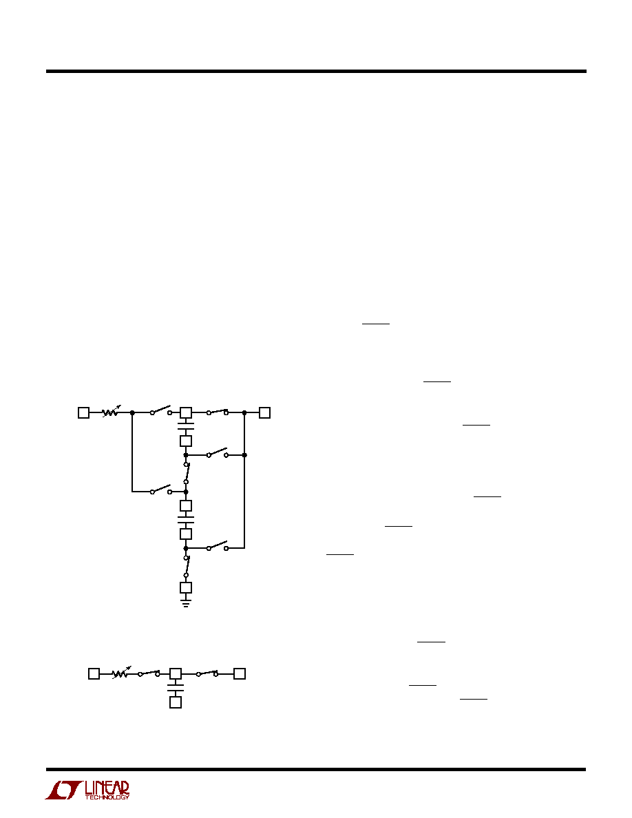
7
LTC1911-1.5/LTC1911-1.8
1911f
transferred to the parallel combination of C1 and C2 is
transferred to the V
OUT
. In this manner, charge is again
transferred from the flying capacitors to the output on
both phases of the clock. As in 2-to-1 mode, charge
current is sourced from GND on phase two of the clock
resulting in increased power efficiency. I
OUT
in 3-to-2
mode equals approximately (3/2)I
IN
.
In 1-to-1 mode (see Figure 1c), switch S1 is always closed
connecting the top plate of C1 to V
OUT
. Switch S2 remains
closed for almost the entire clock period, opening only
briefly at the end of clock phase one. In this manner, V
OUT
is connected to V
IN
through R
A
. The value of R
A
is set by
the regulator control loop which determines the amount of
current transferred to V
OUT
during the on period of S2. The
LTC1911 acts much like a linear regulator in this mode.
Since all of the V
OUT
current is sourced from V
IN
, the
efficiency in 1-to-1 mode is approximately equal to that of
a linear regulator.
Mode Selection
The optimal step-down conversion mode is chosen based
on V
IN
and output load conditions. Two internal compara-
tors are used to select the default step-down mode based
on the input voltage. Each comparator has an adjustable
offset built in that increases (decreases) in proportion to
the increasing (decreasing) output load current. In this
manner, the mode switch point is optimized to provide
peak efficiency over all supply and load conditions. Each
comparator also has built-in hysteresis of about 300mV to
ensure that the LTC1911 does not oscillate between modes
when a transition point is reached.
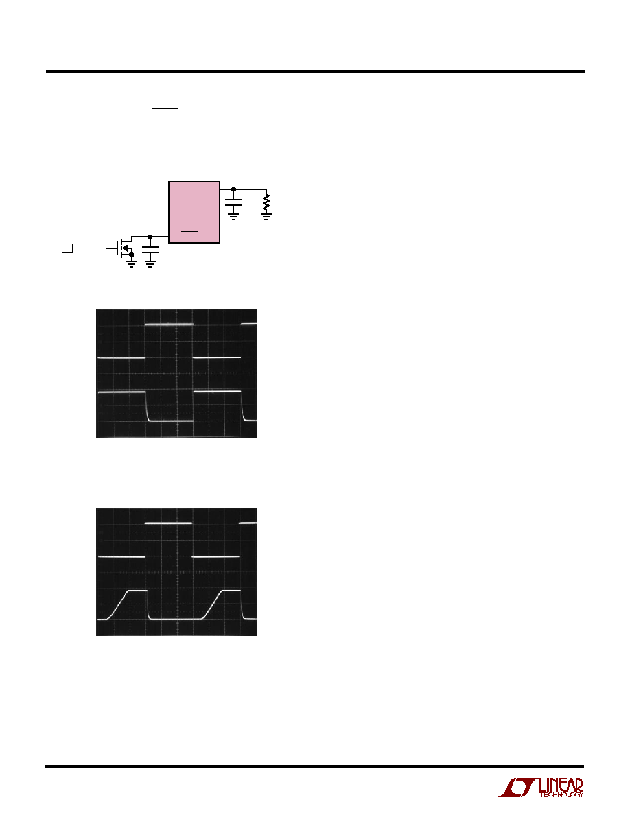
Soft-Start/Shutdown Operation
The SS/SHDN pin is used to implement both low current
shutdown and soft-start. The soft-start feature limits
inrush currents when the regulator is initially powered up
or taken out of shutdown. Forcing a voltage lower than
0.6V (typ) on the SS/SHDN pin will put the LTC1911 into
shutdown mode. Shutdown mode disables all control
circuitry and forces V
OUT
into a high impedance state. A
2
µ
A pull-up current on the SS/SHDN pin will force the part
into active mode if the pin is left floating or is driven with
an open-drain output that is in a high impedance state. If
the pin is not driven with an open-drain device, it must be
forced to a logic high voltage of 2.2V (min) to ensure
proper V
OUT
regulation. The SS/SHDN pin should not be
driven to a voltage higher than V
IN
. To implement soft-
start, the SS/SHDN pin must be driven with an open-drain
device and a capacitor must be connected from the SS/
SHDN pin to GND. Once the open-drain device is turned
off, the 2
µ
A pull-up current will begin charging the external
soft-start capacitor and force the voltage on the pin to
ramp towards V
IN
. As soon as the shutdown threshold is
reached (0.6V typ), the internal reference voltage that
controls the V
OUT
regulation point will follow the ramp
voltage on the SS/SHDN pin (minus a 0.6V offset to
account for the shutdown threshold) until the reference
reaches its final band gap voltage. This occurs when the
voltage on the SS/SHDN pin reaches approximately 1.9V.
Since the ramp rate on the SS/SHDN pin controls the ramp
rate on V
OUT
, the average inrush current can be controlled
through the selection of C
SS
and C
OUT
. For example, a
APPLICATIO S I FOR ATIO
W
U
U
U
V
IN
V
OUT
C1
R
A
C1
+
C1
≠
C2
+
C2
≠
S5
1
S7
1
S4
1
S1
2
S2
2
GND
C2
1911 F01b
S6
1
S3
2
Figure 1b. Step-Down Charge Transfer in 3-to-2 Mode
V
IN
V
OUT
C1
R
A
C1
+
C1
≠
1911 F01c
S2
S1
Figure 1c. Step-Down Charge Transfer in 1-to-1 Mode
8
LTC1911-1.5/LTC1911-1.8
1911f
4.7nF capacitor on SS/SHDN results in a 3ms ramp time
from 0.6V to 1.9V on the pin. If C
OUT
is 10
µ
F, the 3ms V
REF
ramp time results in an average C
OUT
charge current of
only 6mA (see Figure 2).
Low Current Burst Mode Operation
To improve efficiency at low output currents, a Burst Mode
function was included in the design of the LTC1911. An
output current sense circuit is used to detect when the
required output current drops below 30mA typ. When this
occurs, the oscillator shuts down and the part goes into a
low current operating state. The LTC1911 will remain in
the low current operating state until V
OUT
has dropped
enough to require another burst of current. Unlike tradi-
tional charge pumps who's burst current is dependant on
many factors (i.e., supply, switch strength, capacitor
selection, etc.), the LTC1911 burst current is set by the
burst threshold. This means that the
output ripple voltage
during Burst Mode operaton will be fixed and is typically
5mV for C
OUT
= 10
µ
F.
Short-Circuit/Thermal Protection
The LTC1911 has built-in short-circuit current limiting as
well as overtemperature protection. During short-circuit
conditions it will automatically limit its output current to
approximately 600mA. The LTC1911 will shut down if the
junction temperature exceeds approximately 160
∞
C. Un-
der normal operating conditions, the LTC1911 should not
go into thermal shutdown but it is included to protect the
IC in cases of excessively high ambient temperatures, or
in cases of excessive power dissipation inside the IC (i.e.,
overcurrent or short circuit). The charge transfer will
reactivate once the junction temperature drops back to
approximately 150
∞
C. The LTC1911 can cycle in and out
of thermal shutdown indefinitely without latch-up or
damage until the fault condition is removed.
V
OUT
Ripple and Capacitor Selection
The type and value of capacitors used with the
LTC1911 determine several important parameters such
as regulator control loop stability, output ripple and
charge pump strength.
The value of C
OUT
directly controls the amount of output
ripple for a given load current. Increasing the size of C
OUT
will reduce the output ripple.
APPLICATIO S I FOR ATIO
W
U
U
U
Figure 2. Shutdown/Soft-Start Operation
SS/SHDN
C
SS
ON OFF V
CTRL
6
8
V
OUT
R
LOAD
LTC1911
C
OUT
(2a)
V
CTRL
2V/DIV
V
OUT
1V/DIV
C
SS
= 0nF
2ms/DIV
1911 F02b
C
OUT
= 10
µ
F
R
LOAD
= 10
(2b)
V
CTRL
2V/DIV
V
OUT
1V/DIV
C
SS
= 4.7nF
2ms/DIV
1911 F02c
C
OUT
= 10
µ
F
R
OUT
= 10
(2c)

9
LTC1911-1.5/LTC1911-1.8
1911f
To reduce output noise and ripple, it is suggested that a
low ESR (
0.1
) ceramic capacitor (10
µ
F
or greater) be
used for C
OUT
. Tantalum and Aluminum capacitors are not
recommended because of their high ESR (equivalent
series resistance).
Both the style and value of C
OUT
can significantly affect the
stability of the LTC1911. As shown in the Block Diagram,
the part uses a control loop to adjust the strength of the
charge pump to match the current required at the output.
The error signal of this loop is stored directly on the output
charge storage capacitor. The charge storage capacitor
also serves to form the dominant pole for the control loop.
To prevent ringing or instability it is important for the
output capacitor to maintain at least 4
µ
F of capacitance
over all conditions (See Ceramic Capacitor Selection
Guidelines).
Likewise excessive ESR on the output capacitor will tend
to degrade the loop stability of the LTC1911. The closed-
loop output resistance of the part is designed to be 0.13
.
For a 250mA load current change, the output voltage will
change by about 33mV. If the output capacitor has 0.13
or more of ESR, the closed-loop frequency response will
cease to roll-off in a simple 1-pole fashion and poor load
transient response or instability could result. Ceramic
capacitors typically have exceptional ESR performance,
and combined with a tight board layout, should yield
excellent stability and load transient performance.
V
IN
Capacitor Selection
The constant frequency architecture used by the
LTC1911 makes input noise filtering much less demand-
ing than with conventional regulated charge pumps. De-
pending on the mode of operation the input current of the
LTC1911 can vary from I
OUT
to 0mA on a cycle-by-cycle
basis. Lower ESR will reduce the voltage steps caused by
changing input current, while the absolute capacitor value
will determine the level of ripple. For optimal input noise
and ripple reduction, it is recommended that a low ESR
ceramic capacitor be used for C
IN
. A tantalum capacitor
may be used for C
IN
but the higher ESR will lead to more
input noise. The LTC1911 will operate with capacitors
APPLICATIO S I FOR ATIO
W
U
U
U
less than 1
µ
F but the increasing input noise will feed
through to the output causing degraded performance.
For best performance a 1
µ
F
or greater capacitor is sug-
gested for C
IN
. Aluminum capacitors are not recom-
mended because of their high ESR.
Flying Capacitor Selection
Warning: A polarized capacitor such as tantalum or
aluminum should never be used for the flying capacitors
since their voltage can reverse upon start-up of the
LTC1911. Ceramic capacitors should always be used for
the flying capacitor.
The flying capacitor controls the strength of the charge
pump. In order to achieve the rated output current it is
necessary for the flying capacitor to have at least 0.4
µ
F of
capacitance over operating temperature with a 2V bias
(See Ceramic Capacitor Selection Guidelines). If only
100mA or less of output current is required the flying
capacitor minimum can be reduced to 0.15
µ
F.
Ceramic Capacitor Selection Guidelines
Capacitors of different materials lose their capacitance
with higher temperature and voltage at different rates. For
example, a ceramic capacitor made of X7R material will
retain most of its capacitance from ≠ 40
∞
C to 85
∞
C whereas
a Z5U or Y5V style capacitor will lose considerable capaci-
tance over that range (60% to 80% loss typ). Z5U and Y5V
capacitors may also have a very strong voltage coefficient
causing them to lose an additional 60% or more of their
capacitance when the rated voltage is applied. Therefore,
when comparing different capacitors it is often more
appropriate to compare the amount of achievable capaci-
tance for a given case size rather than discussing the
specified capacitance value. For example, over rated volt-
age and temperature conditions, a 4.7
µ
F, 10V, Y5V ce-
ramic capacitor in a 0805 case may not provide any more
capacitance than a 1
µ
F, 10V, X7R available in the same
0805 case. In fact, over bias and temperature range, the
1
µ
F, 10V, X7R will provide more capacitance than the
4.7
µ
F, 10V, Y5V. The capacitor manufacturer's data sheet
should be consulted to determine what value of capacitor
10
LTC1911-1.5/LTC1911-1.8
1911f
APPLICATIO S I FOR ATIO
W
U
U
U
is needed to ensure that minimum capacitance values are
met over operating temperature and bias voltage.
Table 1 is a list of ceramic capacitor manufacturers and
how to contact them.
Table 1. Ceramic Capacitor Manufacturers
AVX
1-(803)-448-1943
www.avxcorp.com
Kemet
1-(864) 963-6300
www.kemet.com
Murata
1-(800) 831-9172
www.murata.com
Taiyo Yuden
1-(800) 348-2496
www.t-yuden.com
Vishay
1-(800) 487-9437
www.vishay.com
Layout Considerations
Due to the high switching frequency and transient cur-
rents produced by the LTC1911, careful board layout is
necessary for optimal performance. A true ground plane
and short connections to all capacitors will optimize
performance, reduce noise and ensure proper regulation
over all conditions. Figure 3 shows the recommended
layout configuration.
Additional output filtering can be achieved by placing a
second output capacitor, connected to the ground plane,
about 2cm or more from the LTC1911 output capacitor
(C4). The inductance of the trace running to the second
output capacitor will significantly attenuate the high speed
switching transients of the LTC1911. Even small capaci-
tors as low as 0.1
µ
F will provide excellent results.
Thermal Management
The power dissipation in the LTC1911 can cause the
junction temperature to rise at rates of up to 160
∞
C/W. If
the specified operating conditions are followed, the junc-
tion temperature should never exceed the 160
∞
C thermal
shutdown temperature. The junction temperature can
come very close and possibly exceed the specified 125
∞
C
operating junction temperature. To reduce the maximum
junction temperature, a good thermal connection to the PC
board is recommended. Connecting the GND pin (Pin 4) to
a ground plane, and maintaining a solid ground plane
under the device on two layers of the PC board, can reduce
the thermal resistance of the package and PC board
considerably.
C1
1911 F03
C4
OUT
GND
C2
V
IN
SS/SHDN
: CONNECT TO GND PLANE ON BACK OF BOARD
C3
U1
Figure 3. Recommended Component Placement and Grounding
11
LTC1911-1.5/LTC1911-1.8
1911f
U
PACKAGE DESCRIPTIO
MS8 Package
8-Lead Plastic MSOP
(Reference LTC DWG # 05-08-1660)
MSOP (MS8) 0102
0.53
±
0.015
(.021
±
.006)
SEATING
PLANE
NOTE:
1. DIMENSIONS IN MILLIMETER/(INCH)
2. DRAWING NOT TO SCALE
3. DIMENSION DOES NOT INCLUDE MOLD FLASH, PROTRUSIONS OR GATE BURRS.
MOLD FLASH, PROTRUSIONS OR GATE BURRS SHALL NOT EXCEED 0.152mm (.006") PER SIDE
4. DIMENSION DOES NOT INCLUDE INTERLEAD FLASH OR PROTRUSIONS.
INTERLEAD FLASH OR PROTRUSIONS SHALL NOT EXCEED 0.152mm (.006") PER SIDE
5. LEAD COPLANARITY (BOTTOM OF LEADS AFTER FORMING) SHALL BE 0.102mm (.004") MAX
0.18
(.077)
0.254
(.010)
1.10
(.043)
MAX
0.22 ≠ 0.38
(.009 ≠ .015)
0.13
±
0.05
(.005
±
.002)
0.86
(.034)
REF
0.65
(.0256)
BCS
0
∞
≠ 6
∞
TYP
DETAIL "A"
DETAIL "A"
GAUGE PLANE
1
2
3
4
4.88
±
0.1
(.192
±
.004)
8
7 6 5
3.00
±
0.102
(.118
±
.004)
(NOTE 3)
3.00
±
0.102
(.118
±
.004)
NOTE 4
0.52
(.206)
REF
5.23
(.206)
MIN
3.2 ≠ 3.45
(.126 ≠ .136)
0.889
±
0.127
(.035
±
.005)
RECOMMENDED SOLDER PAD LAYOUT
0.42
±
0.04
(.0165
±
.0015)
TYP
0.65
(.0256)
BSC
Information furnished by Linear Technology Corporation is believed to be accurate and reliable.
However, no responsibility is assumed for its use. Linear Technology Corporation makes no represen-
tation that the interconnection of its circuits as described herein will not infringe on existing patent rights.
12
LTC1911-1.5/LTC1911-1.8
1911f
©
LINEAR TECHNOLOGY CORPORATION 2001
LT/TP 1102 2K ∑ PRINTED IN USA
Linear Technology Corporation
1630 McCarthy Blvd., Milpitas, CA 95035-7417
(408) 432-1900
q
FAX: (408) 434-0507
q
www.linear.com
PART NUMBER
DESCRIPTION
COMMENTS
LTC1514
50mA, 650kHz, Step-Up/Down Charge Pump
V
IN
= 2.7V to 10V, V
OUT
= 3V to 5V, I
Q
= 60
µ
A, I
SD
= 10
µ
A,
with Low Battery Comparator
S8 Package
LTC1515
50mA, 650kHz, Step-Up/Down Charge Pump
V
IN
= 2.7V to 10V, V
OUT
= 3.3V or 5V, I
Q
= 60
µ
A, I
SD
= <1
µ
A,
with Power On Reset
S8 Package
LT1776
500mA (I
OUT
), 200kHz, High Efficiency Step-Down
90% Efficiency, V
IN
= 7.4V to 40V, V
OUT
= 1.24V, I
Q
= 3.2mA,
DC/DC Converter
I
SD
= 30
µ
A, N8,S8 Packages
LTC3250-1.5
250mA, 1.5MHz, High Efficiency, Step-Down Charge Pump
85% Efficiency, V
IN
= 3.1V to 5.5V, V
OUT
= 1.5V, I
Q
= 35
µ
A,
I
SD
= <1
µ
A, ThinSOT Package
LTC3251
500mA, 1MHz to 1.6MHz, Spread Spectrum,
85% Efficiency, V
IN
= 3.1V to 5.5V, V
OUT
= 0.9V to 1.6V,
Step-Down Charge Pump
I
Q
= 9
µ
A, I
SD
= <1
µ
A, MS Package
LTC3404
600mA (I
OUT
), 1.4MHz, Synchronous Step-Down
95% Efficiency, V
IN
= 2.7V to 6V, V
OUT
= 0.8V, I
Q
= 10
µ
A,
DC/DC Converter
I
SD
= <1
µ
A, MS8 Package
LTC3405A
300mA (I
OUT
), 1.5MHz, Synchronous Step-Down
95% Efficiency, V
IN
= 2.7V to 6V, V
OUT
= 0.8V, I
Q
= 20
µ
A,
DC/DC Converter
I
SD
= <1
µ
A, ThinSOT Package
LTC3406B
600mA (I
OUT
), 1.5MHz, Synchronous Step-Down
95% Efficiency, V
IN
= 2.5V to 5.5V, V
OUT
= 0.6V, I
Q
= 20
µ
A,
DC/DC Converter
I
SD
= <1
µ
A, ThinSOT Package
LTC3411
1.25A (I
OUT
), 4MHz, Synchronous Step-Down
95% Efficiency, V
IN
= 2.5V to 5.5V, V
OUT
= 0.8V, I
Q
= 60
µ
A,
DC/DC Converter
I
SD
= <1
µ
A, MS Package
LTC3412
2.5A (I
OUT
), 4MHz, Synchronous Step-Down
95% Efficiency, V
IN
= 2.5V to 5.5V, V
OUT
= 0.8V, I
Q
= 60
µ
A,
DC/DC Converter
I
SD
= <1
µ
A, TSSOP16E Package
LTC3440
600mA (I
OUT
), 2MHz, Synchronous Buck-Boost
95% Efficiency, V
IN
= 2.5V to 5.5V, V
OUT
= 2.5V, I
Q
= 25
µ
A,
DC/DC Converter
I
SD
= <1
µ
A, MS Package
ThinSOT is a trademark of Linear Technology Corporation.
TYPICAL APPLICATIO
U
DC/DC Converter with Shutdown and Soft-Start
V
IN
C2
+
C2
≠
GND
8
7
6
5
1
2
3
4
SS/SHDN
C1
+
V
OUT
C1
≠
LTC1911-1.5
1
µ
F*
1-CELL Li-Ion
OR
3-CELL NiMH
10
µ
F*
10
µ
F*
2N7002
ON OFF
10nF
1911 TA03
V
OUT
= 1.5V
I
OUT
= 250mA
1
µ
F*
*CERAMIC CAPACITOR
2.7V TO 5.5V INPUT
RELATED PARTS