1
LTC1921
1921i
Dual ≠48V Supply
and Fuse Monitor
May 2002
The LTC
Æ
1921 monitors two independent ≠ 48V supplies,
including their fuses, and drives up to three optoisolators
to indicate status, in accordance with standard backplane
specifications. Requiring only three noncritical resistors
and optoisolators, the LTC1921 replaces multiple voltage
comparators, a voltage reference and several precision
resistors.
The monitor features dual supply overvoltage and under-
voltage detection circuits. The preset trip thresholds in-
clude overvoltage, undervoltage and undervoltage recovery
that are guaranteed over temperature and meet or exceed
common backplane specifications. Additional built-in cir-
cuitry detects the condition of supply fuses. Overvoltage
and undervoltage detectors ignore fast supply transients,
eliminating false detection. The LTC1921 operates from
≠10V to ≠80V with a typical power dissipation of less than
10mW.
The LTC1921 is available in an 8-pin MSOP package.
s
Independently Monitors Two ≠48V Supplies for
≠ Undervoltage Faults: ≠38.5V
±
1V
MAX
≠ Overvoltage Faults: ≠70V
±
1.5V
MAX
s
Accurately Detects Undervoltage Fault Recovery:
≠43V
±
0.5V
MAX
s
Monitors Two External Fuses
s
Operates from ≠10V to ≠80V
s
Tolerates DC Faults to ≠100V
s
Tolerates Accidental Supply Reversal to 100V
s
Withstands Transient Voltages Up to 200V/≠200V
s
Small Footprint: 8-Lead MSOP Package
s
Requires No Precision External Components
s
Specified from ≠ 40
∞
C to 85
∞
C
s
Telecom Backplanes or Switch Cards
s
Networking Backplanes or Switch Cards
s
High Voltage Fuse Monitoring
, LTC and LT are registered trademarks of Linear Technology Corporation.
Information furnished by Linear Technology Corporation is believed to be accurate and reliable.
However, no responsibility is assumed for its use. Linear Technology Corporation makes no represen-
tation that the interconnection of its circuits as described herein will not infringe on existing patent rights.
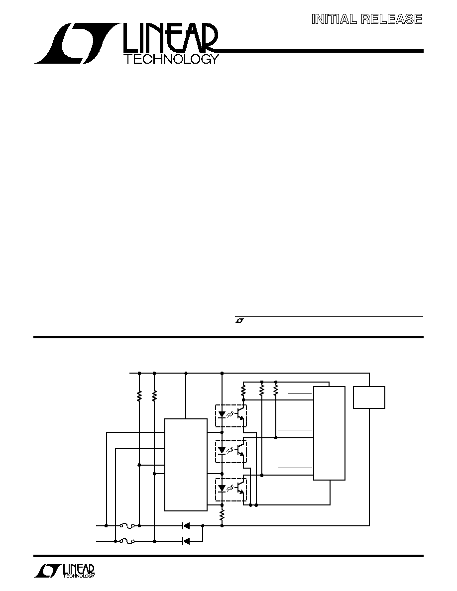
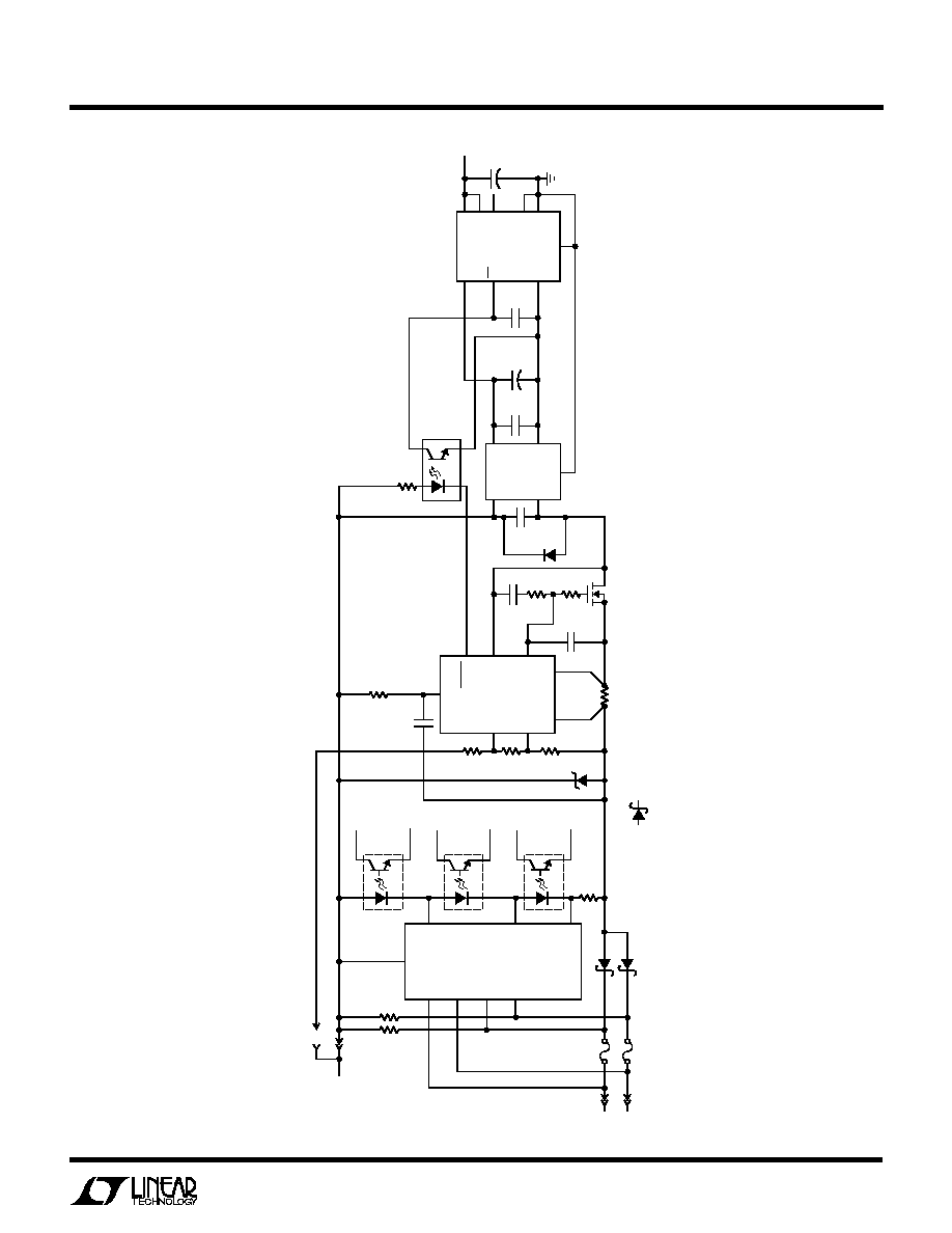
FUSE GOOD
SUPPLY A GOOD
MOC207
MOC207
MOC207
1921 TA01
SUPERVISOR
µ
P
LOGIC
SUPPLY
LOGIC
COMMON
47k
47k
47k
R3
47k
1/4W
SUPPLY B GOOD
OUT F
V
A
3
4
5
7
2
8
1
6
V
B
FUSE A
RTN
LTC1921
FUSE B
OUT A
OUT B
D1 MURS320
F1
SUPPLY A
≠48V
SUPPLY B
≠48V
F2
D2 MURS320
R1
100k
≠ 48V
RETURN
R2
100k
≠48V LOAD
Final Electrical Specifications
FEATURES
DESCRIPTIO
U
APPLICATIO S
U
TYPICAL APPLICATIO
U
2
LTC1921
1921i
(Note 1) All voltages referred to RTN
Supply Voltage
(V
A
, V
B
, FUSE A, FUSE B) ....................... 100V to ≠100V
Transient Voltage (V
A
, V
B
, FUSE A, FUSE B)
(Note 2) ........................................................ 0V to 200V
Transient Voltage (V
A
, V
B
, FUSE A, FUSE B)
(Note 2) ...................................................... 0V to ≠200V
OUT A, OUT B, OUT F Pins ......................... 0.3V to ≠ 8V
Maximum Junction Temperature ......................... 150
∞
C
Operating Temperature Range
LTC1921CMS8 ........................................ 0
∞
C to 70
∞
C
LTC1921IMS8 .................................... ≠ 40
∞
C to 85
∞
C
Storage Temperature Range ................. ≠ 65
∞
C to 150
∞
C
Lead Temperature (Soldering, 10 sec).................. 300
∞
C
ORDER PART
NUMBER
LTC1921CMS8
LTC1921IMS8
T
JMAX
= 150
∞
C,
JA
= 250
∞
C/W
MS8 PART MARKING
LTZV
LTZU
1
2
3
4
V
A
FUSE A
RTN
OUT F
8
7
6
5
V
B
FUSE B
OUT B
OUT A
TOP VIEW
MS8 PACKAGE
8-LEAD PLASTIC MSOP
Consult LTC Marketing for parts specified with wider operating temperature ranges.
The
q
denotes specifications which apply over the full operating
temperature range, otherwise specifications are at T
A
= 25
∞
C. (Note 3) RTN = 0V, V
A
= ≠48V, V
B
= ≠48V, FUSE A = ≠48V,
FUSE B = ≠48V, unless otherwise noted.
ABSOLUTE AXI U RATI GS
W
W
W
U
PACKAGE/ORDER I FOR ATIO
U
U
W
ELECTRICAL CHARACTERISTICS
Note 1: Absolute Maximum Ratings are those values beyond which the life
of a device may be impaired.
Note 2: Transient voltage for less than 10
µ
s. This parameter is not 100%
tested. Voltage should not exceed 200V between any two pins.
Note 3: All currents into device pins are positive; all currents out of device
pins are negative. All voltages are referenced to RTN unless otherwise
specified.
PARAMETER
CONDITIONS
MIN
TYP
MAX
UNITS
Power Supply
Supply Voltage Range (RTN ≠ V
A
, RTN ≠ V
B
)
q
10
80
V
Supply Current (I
A
+ I
B
)
≠160
≠250
µ
A
q
≠300
µ
A
Supply Monitor
Undervoltage Threshold
q
≠39.5
≠37.5
V
Undervoltage Recovery Threshold
q
≠43.5
≠42.5
V
Overvoltage Threshold
q
≠71.5
≠68.5
V
Overvoltage Threshold Hysteresis
q
1
1.6
V
Fuse Monitor
Input Resistance, FUSE A, FUSE B
11
M
Fuse Comparison Threshold |V
FUSEA
≠ V
A
|, |V
FUSEB
≠ V
B
|
2.5
V
LTC1921C
q
0.9
4.5
V
LTC1921I
q
0.5
4.5
V
Output
Propagation Delay
C
OUT
= 100pF, Overdrive = 1V
220
µ
s
Output Switch Resistance, OUT F, OUT A, OUT B
V
A
= V
B
= ≠35V, V
FUSEA
= V
FUSEB
= 0V
25
I
OUT
= 10mA
q
50
Output Switch Off Leakage
500
pA
Output Switch Resistance in Undervoltage Lockout,
V
A
= V
B
= ≠10V, I
OUT
= 10mA
q
60
OUT F, OUT A, OUT B
V
A
= ≠10V, V
B
= 0V, I
OUT
= 10mA
q
80
V
A
= 0V, V
B
= ≠10V, I
OUT
= 10mA
q
80
3
LTC1921
1921i
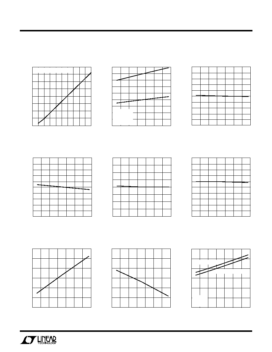
TYPICAL PERFOR A CE CHARACTERISTICS
U
W
Supply Current vs Supply Voltage
SUPPLY VOLTAGE (V)
0
SUPPLY CURRENT (
µ
A)
400
350
300
250
200
150
100
50
0
80
1921 G01
20
40
60
100
70
10
30
50
90
V
A
= V
B
= V
FUSEA
= V
FUSEB
TEMPERATURE (
∞
C)
UNDERVOLTAGE THRESHOLD (V)
1921 G04
≠37.5
≠37.7
≠37.9
≠38.1
≠38.3
≠38.5
≠38.7
≠38.9
≠39.1
≠39.3
≠39.5
≠50
≠30
≠10
10
30
50
70
90
Undervoltage Threshold
vs Temperature
Supply Current vs Temperature
TEMPERATURE (
∞
C)
≠50
SUPPLY CURRENT (
µ
A)
100
I
A
+ I
B
I
A
, I
B
120
140
90
1921 G02
80
60
0
≠30
≠10
10
30
50
70
40
20
180
160
V
A
= ≠48V
V
B
= ≠48V
V
FUSEA
= ≠48V
V
FUSEB
= ≠48V
Undervoltage Recovery Threshold
vs Temperature
TEMPERATURE (
∞
C)
≠50
≠30
≠10
10
UNDERVOLTAGE RECOVERY THRESHOLD (V)
30
50
70
90
1921 G05
≠42.5
≠42.6
≠42.7
≠42.8
≠42.9
≠43.0
≠43.1
≠43.2
≠43.3
≠43.4
≠43.5
Overvoltage Threshold
vs Temperature
TEMPERATURE (
∞
C)
OVERVOLTAGE THRESHOLD (V)
1921 G06
≠68.0
≠68.5
≠69.0
≠69.5
≠70.0
≠70.5
≠71.0
≠71.5
≠72.0
≠50
≠30
≠10
10
30
50
70
90
Overvoltage Hysteresis
vs Temperature
Fuse Window Positive Threshold
vs Temperature
Fuse Window Negative Threshold
vs Temperature
TEMPERATURE (
∞
C)
OVERVOLTAGE HYSTERESIS (V)
1921 G07
1.50
1.45
1.40
1.35
1.30
1.25
1.20
1.15
1.10
1.05
1.00
≠50
≠30
≠10
10
30
50
70
90
TEMPERATURE (
∞
C)
FUSE POSITIVE THRESHOLD (V)
1921 G08
2.7
2.5
2.3
2.1
1.9
1.7
1.5
≠50
≠30
≠10
10
30
50
70
90
TEMPERATURE (
∞
C)
FUSE NEGATIVE THRESHOLD (V)
1921 G09
≠2.0
≠2.2
≠2.4
≠2.6
≠2.8
≠3.0
≠3.2
≠50
≠30
≠10
10
30
50
70
90
Output R
DS(ON)
vs Temperature
TEMPERATURE (
∞
C)
≠50
OUTPUT R
DS(ON)
(
)
20
25
30
10
50
1921 G03
15
10
≠30
≠10
30
70
90
5
0
OUT A (OUT F = 0V)
OUT F, OUT B (OUT A = 0V)
V
A
= ≠35V
V
B
= ≠35V
I = ≠10mA
4
LTC1921
1921i
V
A
(Pin 1): Supply to be Monitored. The voltage at this pin
is compared to the valid supply voltage window and the
result is output at OUT A (Pin 5). Supply current is drawn
from this pin as well as from V
B
(Pin 8).
FUSE A (Pin 2): This pin monitors the state of a fuse by
comparing the voltage at this pin to the voltage at V
A
(Pin 1). The result is output at OUT F (Pin 4).
RTN (Pin 3): Supply Return Reference. This pin must be
at an equal or higher potential than the other pins and
should be wired to the ≠ 48V return.
OUT F (Pin 4): This pin indicates the state of the external
fuses by ORing the comparisons made to the FUSE A and
FUSE B pins. If V
FUSEA
V
A
(V
FUSEA
is within the specified
window around V
A
) and V
FUSEB
V
B
, then OUT F will
exhibit a high internal impedance to the RTN pin. If
V
FUSEA
V
A
or V
FUSEB
V
B
, then OUT F is shorted
internally to the RTN pin and can shunt enough current to
turn off an optocoupler or LED wired between these pins.
OUT F should be clamped externally so that it cannot be
driven more than 8V below RTN. This is done automati-
cally by the optocoupler or LED diodes shown in the
application circuits.
OUT A (Pin 5): Indicates the State of V
A
. If V
A
is within the
specified voltage window (neither undervoltage nor over-
voltage), OUT A will exhibit a high internal impedance to the
U
U
U
PI FU CTIO S
TYPICAL PERFOR A CE CHARACTERISTICS
U
W
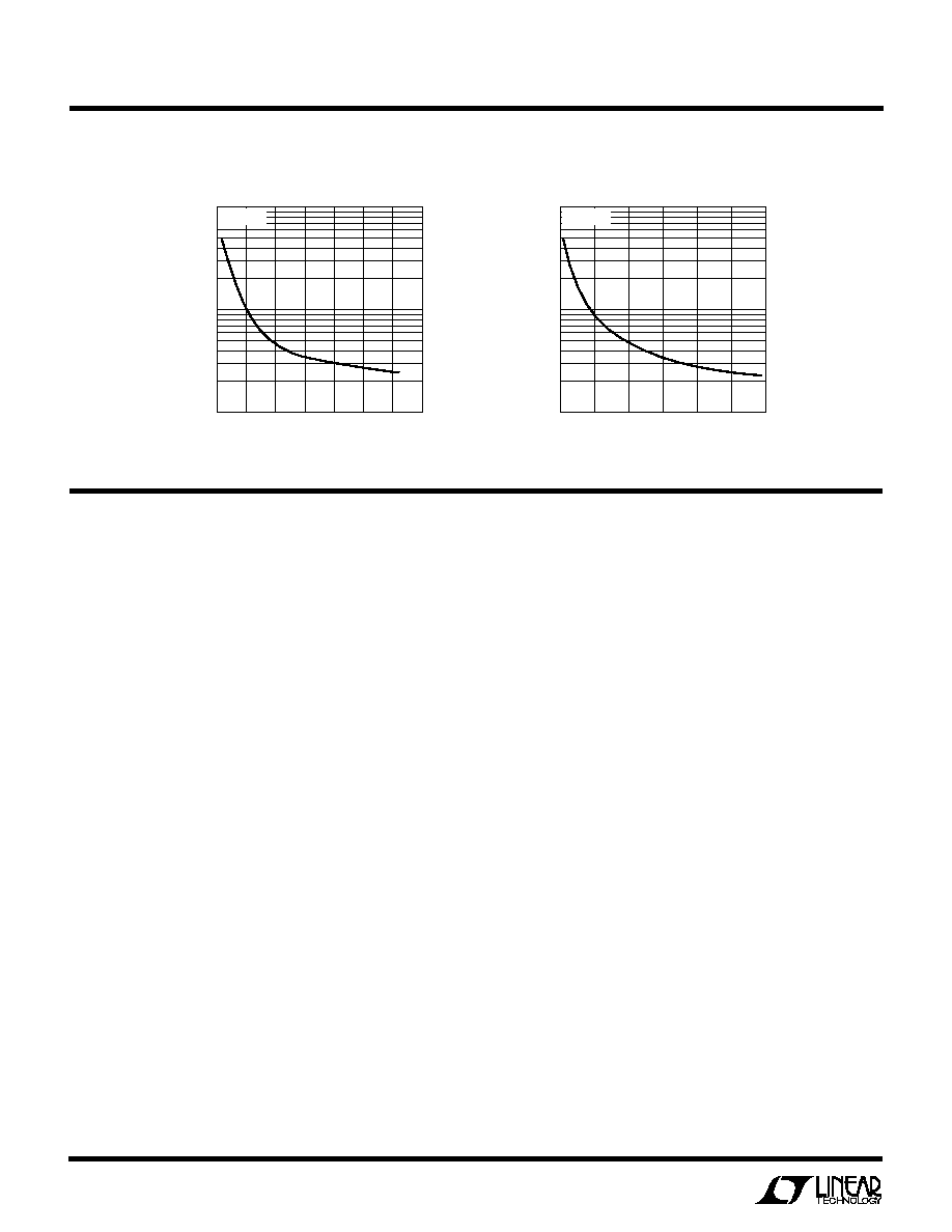
Undervoltage Response Time
OUT F pin. If V
A
is outside the specified overvoltage or
undervoltage limits, then OUT A is shorted internally to the
OUT F pin and can shunt enough current to turn off an
optocoupler or LED wired between these pins. OUT A should
be clamped externally so that it cannot be driven more than
8V below RTN. This is done automatically by the
optocoupler or LED diodes shown in the application circuits.
OUT B (Pin 6): Indicates the State of V
B
. If V
B
is within the
specified voltage window (neither undervoltage nor over-
voltage), OUT B will exhibit a high internal impedance to the
OUT A pin. If V
B
is outside the specified overvoltage or
undervoltage limits, then OUT B is shorted internally to the
OUT A pin and can shunt enough current to turn off an
optocoupler or LED wired between these pins. OUT B should
be clamped externally so that it cannot be driven more than
8V below RTN. This is done automatically by the
optocoupler or LED diodes shown in the application circuits.
FUSE B (Pin 7): This pin monitors the state of a fuse by
comparing the voltage at this pin to the voltage at V
B
(Pin 8). The result is output at OUT F (Pin 4).
V
B
(Pin 8): Supply to be Monitored. The voltage at this pin
is compared to the valid supply voltage window and the
result is output at OUT B (Pin 6). Supply current is drawn
from this pin as well as from V
A
(Pin 1).
SUPPLY STEP FROM UNDERVOLTAGE
RECOVERY THRESHOLD (V)
4.6
10000
4.8
1921 G10
RESPONSE TIME (
µ
s)
4.5
5.2
4.7
4.9
5.0
5.1
100
1000
T
A
= 25
∞
C
SUPPLY STEP FROM OVERVOLTAGE
RECOVERY THRESHOLD (V)
1.5
10000
1.9
1921 G11
RESPONSE TIME (
µ
s)
1.3
2.5
1.7
2.1
2.3
100
1000
T
A
= 25
∞
C
Overvoltage Response Time
5
LTC1921
1921i
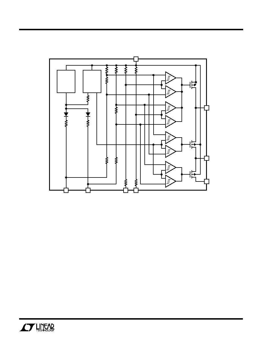
BLOCK DIAGRA
W
7
2
FUSE A
8
V
B
1
V
A
FUSE B
6
OUT B
1921 BD
5
OUT A
4
OUT F
REF
REGULATOR
3
RTN
+
≠
+
≠
+
≠
+
≠
+
≠
+
≠
+
≠
+
≠
6
LTC1921
1921i
Supply Monitoring
The LTC1921 is designed to monitor dual ≠ 48V power
supplies. This is accomplished with precision window
comparators and an accurate bandgap reference, as well
as internal level shifting circuitry. The comparators are
preset to standard voltage thresholds in order to accu-
rately verify the status of each supply. These comparators
also include precision hysteresis which allows accurate
determination of voltage recovery. Status of the two
supplies are indicated by the OUT A and OUT B pins.
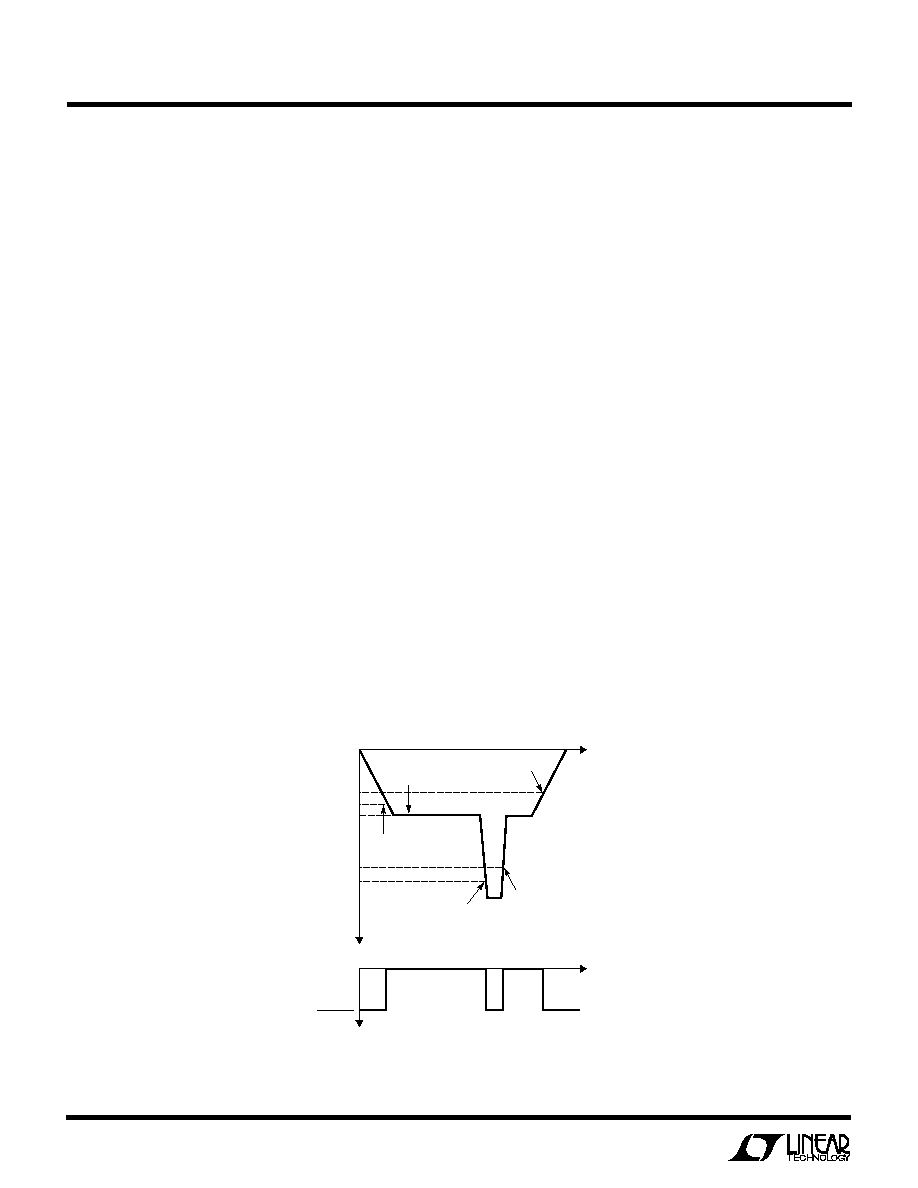
The supply window comparison works in a straightfor-
ward way (Figure 1). As long as each supply magnitude
remains in the valid supply window (38.5V to 70V), the
outputs will indicate a valid supply condition by exhibiting
a high internal impedance. If a supply magnitude falls
below the undervoltage threshold (38.5V), then its respec-
tive output will short internally (OUT A to OUT F or OUT B
to OUT A) until that supply reaches the undervoltage
recovery threshold, which is preset to ≠43V. At this time,
the output will return to a high impedance state. If a supply
magnitude rises above the overvoltage threshold (70V),
then its respective output will short internally, just as with
an undervoltage condition. The output will return to its
nominal state when the supply overcomes the overvoltage
hysteresis.
APPLICATIO S I FOR ATIO
W
U
U
U
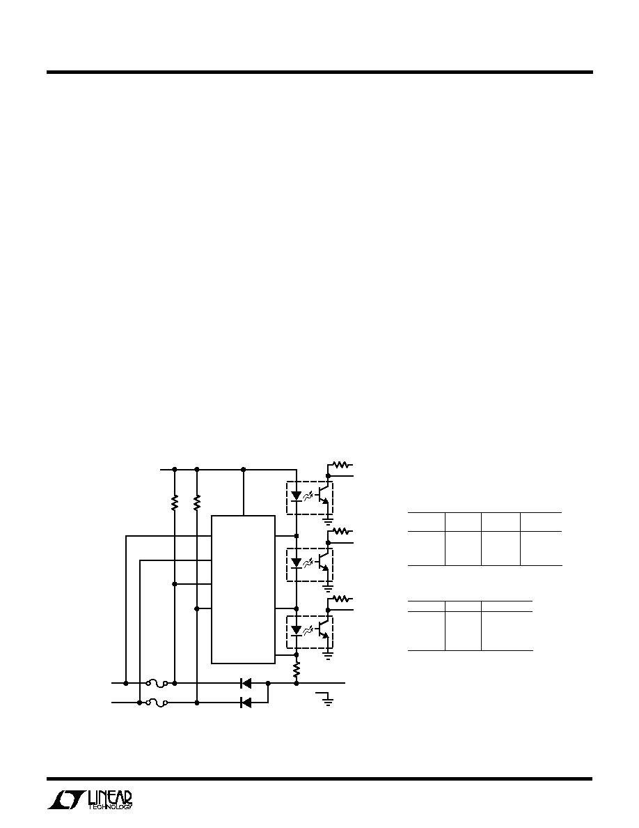
Monitoring for each supply, V
A
and V
B
, is independent of
the condition of the other supply. The LTC1921 can be
powered equally from either V
A
, V
B
or both supplies. This
allows the LTC1921 to provide correct information at its
outputs as long as at least one supply is functional,
whether or not the fuses are intact (see Figure 2).
Undervoltage Lockout
If both supplies are active and their magnitude falls below
13V, or if only one supply is active and its magnitude falls
below 19V, the LTC1921 will lock all outputs into a fault
condition by closing all three output switches. This state
will be held until one supply magnitude is driven above
19V or both are driven above 13V.
Fuse Monitoring
In addition to monitoring two supplies, the LTC1921 can
monitor the condition of two supply fuses via the FUSE A
(Pin 2) and FUSE B (Pin 7) inputs. Fuse monitoring is
accomplished by comparing the potential at FUSE A to the
potential at supply V
A
and comparing the potential at
FUSE B to the potential at supply V
B
. If V
FUSEA
is within the
specified voltage window around V
A
and V
FUSEB
is within
the specified voltage window around V
B
, the OUT F pin will
indicate that the fuses are intact by exhibiting a high
0
0
V
SUPPLY
R3
≠38.5
≠43
≠48
≠68.7
≠70
1921 F01
TIME
NOMINAL
VOLTAGE
UNDERVOLTAGE
RECOVERY
OVERVOLTAGE
FAULT
OVERVOLTAGE
RECOVERY
UNDERVOLTAGE
FAULT
SUPPLY VOLTAGE (V)
I
OUT
(A)
Figure 1. Supply Comparison
7
LTC1921
1921i
internal impedance to the return (RTN) pin. The applica-
tion must be designed so that an open fuse condition will
force the fuse input (FUSE A or FUSE B) to be outside the
specified window around the supply pins, such as with a
weak pull-up resistor to RTN, so that the LTC1921 can
properly indicate a fault at OUT F. If supply diodes that
exhibit high reverse leakage, such as Schottky diodes, are
used, then the values of the pull-up resistors must be
reduced accordingly.
The FUSE A and FUSE B pins may also be used in
conjunction with V
A
and V
B
for simple window compari-
son, provided that one of the circuit nodes to be compared
can provide the small amount of supply current required to
bias the IC. The LTC1921 is ideally suited for comparison
functions in a circuit where only high supply voltages are
available.
Output Pins
The output pins in the LTC1921 are designed to shunt
external optocoupler diodes or LEDs during a supply or
fuse fault condition. Up to three diodes may be used in
series, one for each output. In this configuration
(Figure 2), a diode connected between OUT F and RTN will
indicate the condition of both fuses. A diode connected
between OUT A and OUT F will indicate the condition of
supply A (V
A
) and a diode connected between OUT B and
OUT A will indicate the condition of supply B (V
B
). A
resistor connected from OUT B to the negative supply is
required to bias the diodes. The LTC1921 is designed to
allow the current from this resistor to flow through the
diodes during normal supply conditions and intact fuses,
and will shunt this current away from the proper diodes
during a fault condition. These diodes will further clamp
the output pin potentials to RTN in order to keep the
outputs within rated voltages. If LEDs are used instead of
optocouplers, they should be green since they will be lit
when the supplies are within the proper voltage range.
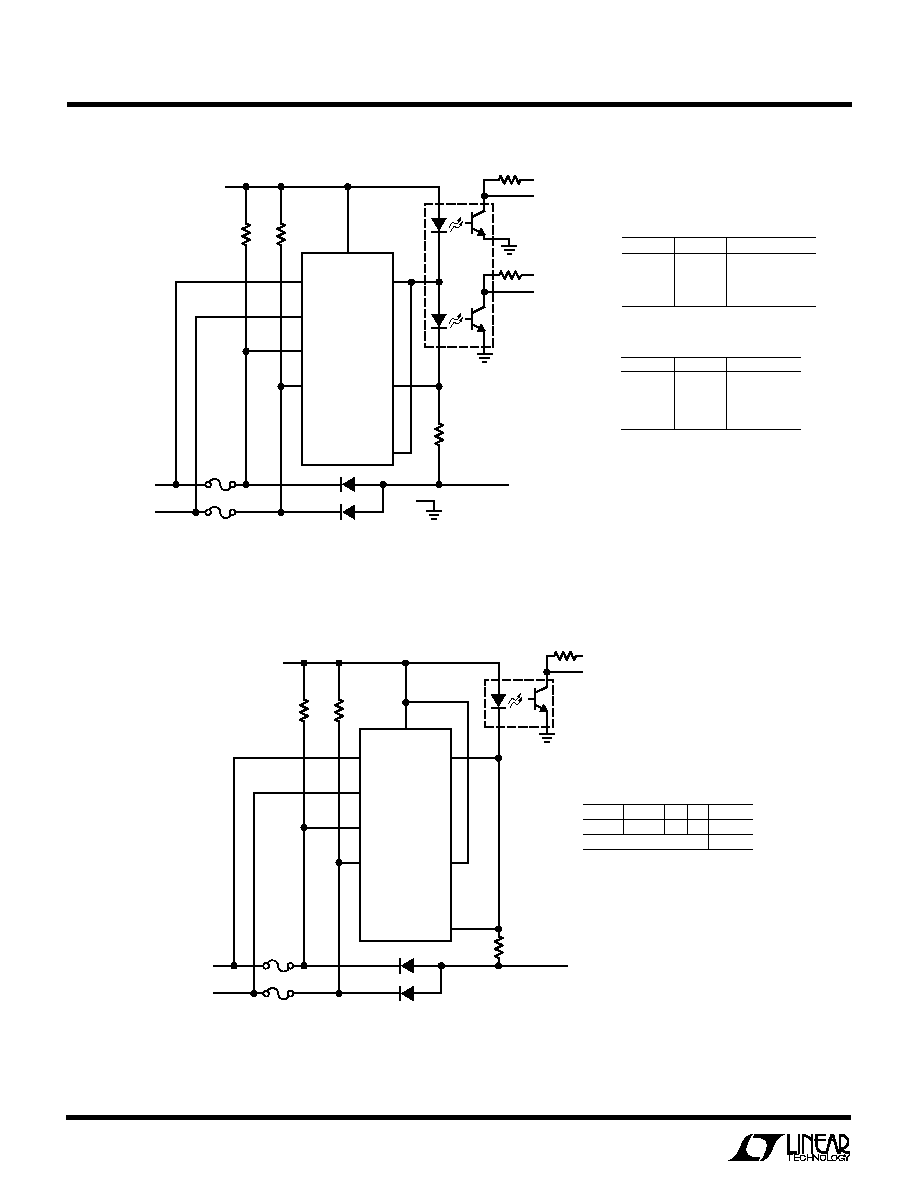
The LTC1921 may be connected in such a way as to OR
various outputs to allow the use of fewer optocouplers or
LEDs (Figures 3a and 3b). One and two diode circuits are
shown.
APPLICATIO S I FOR ATIO
W
U
U
U
MOC207
MOC207
MOC207
FUSE
STATUS
SUPPLY A
STATUS
1921 F02
5V
47k
5V
47k
5V
47k
R3
47k
1/4W
SUPPLY B
STATUS
OK: WITHIN SPECIFICATION
OV: OVERVOLTAGE
UV: UNDERVOLTAGE
≠48V OUT
= LOGIC COMMON
0: LED/PHOTODIODE ON
1: LED/PHOTODIODE OFF
*IF BOTH FUSES (F1 AND F2) ARE OPEN,
ALL STATUS OUTPUTS WILL BE HIGH
SINCE R3 WILL NOT BE POWERED
OUT F
≠48V
RETURN
V
A
3
4
5
7
2
8
1
6
V
B
FUSE A
F1
D1
D2
F2
RTN
LTC1921
FUSE B
OUT A
OUT B
SUPPLY A
≠48V
SUPPLY B
≠48V
R1
100k
R2
100k
SUPPLY A
STATUS
0
0
1
1
V
B
OK
UV OR OV
OK
UV OR OV
V
A
OK
OK
UV OR OV
UV OR OV
SUPPLY B
STATUS
0
1
0
1
FUSE STATUS
0
1
1
1*
FUSE B
= V
B
V
B
= V
B
V
B
FUSE A
= V
A
= V
A
V
A
V
A
Figure 2
8
LTC1921
1921i
MOCD207
FUSE STATUS
SUPPLY
STATUS
1921 F03a
5V
47k
5V
47k
R3
47k
1/4W
≠48V OUT
OUT F
≠48V
RETURN
V
A
3
4
5
7
2
8
1
6
V
B
FUSE A
RTN
LTC1921
FUSE B
OUT A
OUT B
SUPPLY A
≠48V
SUPPLY B
≠48V
R1
100k
F1
F2
R2
100k
OK: WITHIN SPECIFICATION
OV: OVERVOLTAGE
UV: UNDERVOLTAGE
0: LED/PHOTODIODE ON
1: LED/PHOTODIODE OFF
*IF BOTH FUSES (F1 AND F2) ARE OPEN,
ALL STATUS OUTPUTS WILL BE HIGH
SINCE R3 WILL NOT BE POWERED
SUPPLY STATUS
0
1
1
1
V
B
OK
UV OR OV
OK
UV OR OV
V
A
OK
OK
UV OR OV
UV OR OV
FUSE STATUS
0
1
1
1*
FUSE B
= V
B
V
B
= V
B
V
B
FUSE A
= V
A
= V
A
V
A
V
A
= LOGIC COMMON
MOC207
STATUS
1921 F03b
5V
OK: WITHIN SPECIFICATION
0: LED/PHOTODIODE ON
1: LED/PHOTODIODE OFF
47k
LOGIC
COMMON
48k
1/2W
≠48V OUT
OUT F
V
A
3
4
5
7
2
8
1
6
V
B
FUSE A
RTN
LTC1921
FUSE B
OUT A
OUT B
SUPPLY A
≠48V
SUPPLY B
≠48V
100k
≠48V
RETURN
100k
FUSE B
= V
B
V
A
OK
V
B
OK
STATUS
0
1
FUSE A
= V
A
ALL OTHER CONDITIONS
Figure 3a. Combined Supply Status
Figure 3b. All Outputs Combined
APPLICATIO S I FOR ATIO
W
U
U
U
9
LTC1921
1921i
TYPICAL APPLICATIO S
U
+
V
EE
V
DD
C8
100nF
100V
LT4250L
PWRGD
SENSE
C1
470nF
25V
C2
15nF
100V
C3
0.1
µ
F
100V
C4
0.1
µ
F
100V
C6
0.1
µ
F
100V
C5
100
µ
F
100V
C7
100
µ
F
16V
Q1
IRF530
R2
10
5%
R3
1k
5%
R8
100
R4
549k
1%
R5
6.49k
1%
R6
10k
1%
R1
0.02
5%
4
OV
3
2
≠
48V A
≠
48V
RTN
≠
48V B
UV
5
6
8
7
1
GATE
DRAIN
LUCENT
JW050A1-E
V
OUT
+
SENSE
+
TRIM
SENSE
≠
V
OUT
≠
V
IN
+
9
5V
1921 TA02
8
7
6
5
3
1
2
4
ON/OFF
CASE
V
IN
≠
V
OUT
+
V
OUT
≠
V
IN
+
CASE
V
IN
≠
1N4003
+
LUCENT
FLTR100V10
*
* DIODES INC. SMAT70A
MOC207
R7
51k
5%
MOC207
MOC207
MOC207
FUSE
STATUS
SUPPLY A
STATUS
R11
47k
1/4W
SUPPLY B
STATUS
OUT F
V
A
3
4
5
7
2
8
1
6
V
B
FUSE A
3A
3A
RTN
LTC1921
FUSE B
OUT A
OUT B
R10
10k
1W
R9
10k
1W
= DIODES INC. B3100
Complete
≠
48V Telecom Supply Monitor and Hot Swap
TM
Controller
Hot Swap is a trademark of Linear Technology Corporation.
10
LTC1921
1921i
TYPICAL APPLICATIO S
U
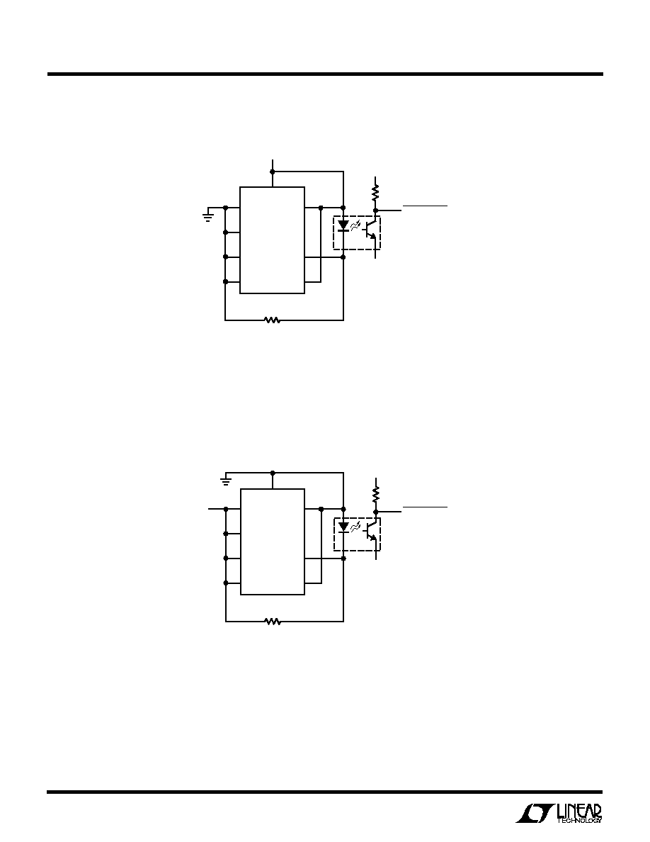
Single 48V Supply Monitor
MOC207
1921 TA04
LOGIC V
+
LOGIC
COMMON
SUPPLY GOOD
47k
OUT F
V
A
3
4
5
7
47k
1/4W
2
8
1
6
V
B
FUSE A
RTN
V
+
LTC1921
FUSE B
OUT A
OUT B
Single ≠48V Supply Monitor
MOC207
1921 TA06
LOGIC V
+
LOGIC
COMMON
SUPPLY GOOD
47k
OUT F
V
A
V
≠
3
4
5
7
47k
1/4W
2
8
1
6
V
B
FUSE A
RTN
LTC1921
FUSE B
OUT A
OUT B
11
LTC1921
1921i
U
PACKAGE DESCRIPTIO
MS8 Package
8-Lead Plastic MSOP
(Reference LTC DWG # 05-08-1660)
MSOP (MS8) 1001
0.53
±
0.015
(.021
±
.006)
SEATING
PLANE
NOTE:
1. DIMENSIONS IN MILLIMETER/(INCH)
2. DRAWING NOT TO SCALE
3. DIMENSION DOES NOT INCLUDE MOLD FLASH, PROTRUSIONS OR GATE BURRS.
MOLD FLASH, PROTRUSIONS OR GATE BURRS SHALL NOT EXCEED 0.152mm (.006") PER SIDE
4. DIMENSION DOES NOT INCLUDE INTERLEAD FLASH OR PROTRUSIONS.
INTERLEAD FLASH OR PROTRUSIONS SHALL NOT EXCEED 0.152mm (.006") PER SIDE
5. LEAD COPLANARITY (BOTTOM OF LEADS AFTER FORMING) SHALL BE 0.102mm (.004") MAX
0.18
(.077)
0.254
(.010)
1.10
(.043)
MAX
0.22 ≠ 0.38
(.009 ≠ .015)
0.13
±
0.05
(.005
±
.002)
0.86
(.034)
REF
0.65
(.0256)
BCS
0
∞
≠ 6
∞
TYP
DETAIL "A"
DETAIL "A"
GAUGE PLANE
1
2
3
4
4.88
±
0.1
(.192
±
.004)
8
7 6 5
3.00
±
0.102
(.118
±
.004)
(NOTE 3)
3.00
±
0.102
(.118
±
.004)
NOTE 4
0.52
(.206)
REF
5.23
(.206)
MIN
3.2 ≠ 3.45
(.126 ≠ .136)
0.889
±
0.127
(.035
±
.005)
RECOMMENDED SOLDER PAD LAYOUT
0.42
±
0.04
(.0165
±
.0015)
TYP
0.65
(.0256)
BSC
12
LTC1921
1921i
Linear Technology Corporation
1630 McCarthy Blvd., Milpitas, CA 95035-7417
(408) 432-1900
q
FAX: (408) 434-0507
q
www.linear.com
©
LINEAR TECHNOLOGY CORPORATION 2002
LT/TP 0502 1.5K ∑ PRINTED IN USA
RELATED PARTS
PART NUMBER
DESCRIPTION
COMMENTS
LT4250
≠48V Hot Swap Controller in SO-8 Package
Active Current Limiting, Supplies from ≠20V to ≠80V
LTC4251
≠48V Hot Swap Controller in SOT-23 Package
Fast Active Current Limiting, Supplies from ≠15V (Floating)
LTC4252
≠48V Hot Swap Controller in MSOP Package
Fast Active Current Limiting, Floating Supply, PWRGD Output
LTC4253
≠48V Hot Swap Controller with Sequencer
Similar to LTC4252, Sequences Three DC/DC Converters
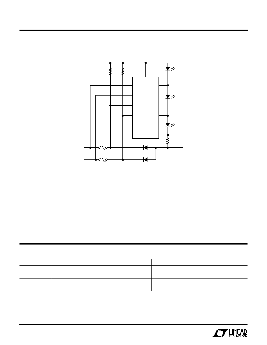
TYPICAL APPLICATIO
U
1921 TA03
R3
5.1k
2W
D5
GREEN
D4
GREEN
D3
GREEN
OUT F
≠48V RETURN
V
A
3
4
5
7
2
8
1
6
≠48V OUT
V
B
FUSE A
RTN
LTC1921
FUSE B
OUT A
OUT B
D1
F1
SUPPLY A
≠48V
SUPPLY B
≠48V
F2
D2
R2
100k
R1
100k
Voltage and Fuse Monitor with LED Outputs