 | ÐлекÑÑоннÑй компоненÑ: LTC1921I | СкаÑаÑÑ:  PDF PDF  ZIP ZIP |
1921f.pm6

LTC1921
1
1921f
Dual 48V Supply
and Fuse Monitor
, LTC and LT are registered trademarks of Linear Technology Corporation.
The LTC
®
1921 monitors two independent 48V supplies,
including their fuses, and drives up to three optoisolators
to indicate status, in accordance with standard backplane
specifications. Requiring only three noncritical resistors
and optoisolators, the LTC1921 replaces multiple voltage
comparators, a voltage reference and several precision
resistors.
The monitor features dual supply overvoltage and under-
voltage detection circuits. The preset trip thresholds in-
clude overvoltage, undervoltage and undervoltage recovery
that are guaranteed over temperature and meet or exceed
common backplane specifications. Additional built-in cir-
cuitry detects the condition of supply fuses. Overvoltage
and undervoltage detectors ignore fast supply transients,
eliminating false detection. The LTC1921 operates from
10V to 80V with a typical power dissipation of less than
10mW.
The LTC1921 is available in 8-pin MSOP and SOIC pack-
ages.
s
Withstands Transient Voltages Up to 200V/200V
s
Requires No Precision External Components
s
Independently Monitors Two 48V Supplies for
Undervoltage Faults: 38.5V
±
1V
MAX
Overvoltage Faults: 70V
±
1.5V
MAX
s
Accurately Detects Undervoltage Fault Recovery:
43V
±
0.5V
MAX
s
Monitors Two External Fuses
s
Operates from 10V to 80V
s
Tolerates DC Faults to 100V
s
Tolerates Accidental Supply Reversal to 100V
s
Small Footprint: 8-Lead MSOP Package
s
Specified from 40
°
C to 85
°
C
s
Telecom Backplanes or Switch Cards
s
Networking Backplanes or Switch Cards
s
High Voltage Fuse Monitoring
FEATURES
APPLICATIO S
U
DESCRIPTIO
U
TYPICAL APPLICATIO
U
FUSE GOOD
SUPPLY A GOOD
MOC207
MOC207
MOC207
1921 TA01
SUPERVISOR
µ
P
LOGIC
SUPPLY
LOGIC
COMMON
47k
47k
47k
R3
47k
1/4W
SUPPLY B GOOD
OUT F
V
A
3
4
5
7
2
8
1
6
V
B
FUSE A
RTN
LTC1921
FUSE B
OUT A
OUT B
D1 MURS320
F1
SUPPLY A
48V
SUPPLY B
48V
F2
D2 MURS320
R1
100k
48V
RETURN
R2
100k
48V LOAD

LTC1921
2
1921f
ABSOLUTE AXI U
RATI GS
W
W
W
U
PACKAGE/ORDER I FOR ATIO
U
U
W
(Note 1) All voltages referred to RTN
Supply Voltage
(V
A
, V
B
, FUSE A, FUSE B) ....................... 100V to 100V
Transient Voltage (V
A
, V
B
, FUSE A, FUSE B)
(Note 2) ........................................................ 0V to 200V
Transient Voltage (V
A
, V
B
, FUSE A, FUSE B)
(Note 2) ...................................................... 0V to 200V
OUT A, OUT B, OUT F Pins ......................... 0.3V to 8V
ORDER PART
NUMBER
LTC1921CMS8
LTC1921IMS8
T
JMAX
= 150
°
C,
JA
= 300
°
C/W
MS8 PART MARKING
LTZV
LTZU
Consult LTC Marketing for parts specified with wider operating temperature ranges.
The
q
denotes specifications which apply over the full operating
temperature range, otherwise specifications are at T
A
= 25
°
C. (Note 5) RTN = 0V, V
A
= 48V, V
B
= 48V, FUSE A = 48V,
FUSE B = 48V, unless otherwise noted.
PARAMETER
CONDITIONS
MIN
TYP
MAX
UNITS
Power Supply
Supply Voltage Range (RTN V
A
, RTN V
B
)
q
10
80
V
Supply Current (I
A
+ I
B
)
160
250
µ
A
q
300
µ
A
Supply Monitor
Undervoltage Threshold
q
39.5
37.5
V
Undervoltage Recovery Threshold
q
43.5
42.5
V
Overvoltage Threshold
q
71.5
68.5
V
Overvoltage Threshold Hysteresis
q
1
1.6
V
Fuse Monitor
Input Resistance, FUSE A, FUSE B
11
M
Fuse Comparison Threshold |V
FUSEA
V
A
|, |V
FUSEB
V
B
|
V
LTC1921C
q
0.9
4.5
V
LTC1921I
q
0.5
4.5
V
Output
Propagation Delay
C
OUT
= 100pF, Overdrive = 1V
220
µ
s
Output Switch Resistance, OUT F, OUT A, OUT B
V
A
= V
B
= 35V, V
FUSEA
= V
FUSEB
= 0V
25
I
OUT
= 10mA
q
50
Maximum Junction Temperature ......................... 150
°
C
Operating Temperature Range (Note 3)
LTC1921C/LTC1921I .......................... 40
°
C to 85
°
C
Specified Temperature Range (Note 4)
LTC1921C/LTC1921I .......................... 40
°
C to 85
°
C
Storage Temperature Range ................. 65
°
C to 150
°
C
Lead Temperature (Soldering, 10 sec).................. 300
°
C
ORDER PART
NUMBER
LTC1921CS8
LTC1921IS8
S8 PART MARKING
1921
1921I
ELECTRICAL CHARACTERISTICS
1
2
3
4
V
A
FUSE A
RTN
OUT F
8
7
6
5
V
B
FUSE B
OUT B
OUT A
TOP VIEW
MS8 PACKAGE
8-LEAD PLASTIC MSOP
1
2
3
4
8
7
6
5
TOP VIEW
V
B
FUSE B
OUT B
OUT A
V
A
FUSE A
RTN
OUT F
S8 PACKAGE
8-LEAD PLASTIC SO
T
JMAX
= 150
°
C,
JA
= 190
°
C/W
LTC1921
3
1921f
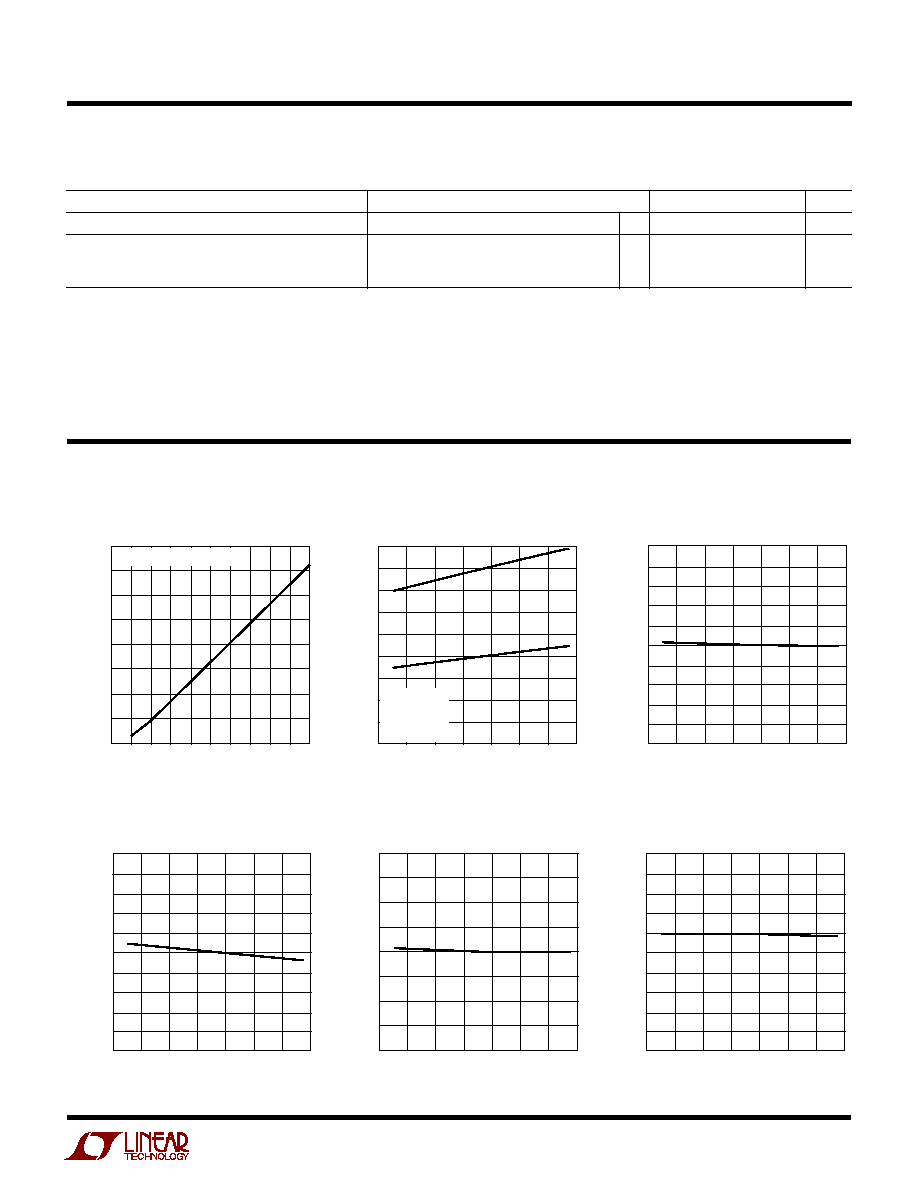
Supply Current vs Supply Voltage
Undervoltage Threshold
vs Temperature
Supply Current vs Temperature
Undervoltage Recovery Threshold
vs Temperature
Overvoltage Threshold
vs Temperature
Overvoltage Hysteresis
vs Temperature
Note 1: Absolute Maximum Ratings are those values beyond which the life
of a device may be impaired.
Note 2: Transient voltage for less than 10
µ
s. This parameter is not 100%
tested. Voltage should not exceed 200V between any two pins.
Note 3: The LTC1921C and LTC1921I are guaranteed functional over the
operating temperature range of 40
°
C to 85
°
C.
The
q
denotes specifications which apply over the full operating
temperature range, otherwise specifications are at T
A
= 25
°
C. (Note 5) RTN = 0V, V
A
= 48V, V
B
= 48V, FUSE A = 48V,
FUSE B = 48V, unless otherwise noted.
Note 4: The LTC1921C is guaranteed to meet specified performance from
0
°
C to 70
°
C. The LTC1921C is designed, characterized and expected to
meet specified performance from 40
°
C to 85
°
C but is not tested or QA
sampled at these temperatures. The LTC1921I is guaranteed to meet
specified performance from 40 t0 85
°
C.
Note 5: All currents into device pins are positive; all currents out of device
pins are negative. All voltages are referenced to RTN unless otherwise
specified.
PARAMETER
CONDITIONS
MIN
TYP
MAX
UNITS
Output Switch Off Leakage
500
pA
Output Switch Resistance in Undervoltage Lockout,
V
A
= V
B
= 10V, I
OUT
= 10mA
q
60
OUT F, OUT A, OUT B
V
A
= 10V, V
B
= 0V, I
OUT
= 10mA
q
80
V
A
= 0V, V
B
= 10V, I
OUT
= 10mA
q
80
ELECTRICAL CHARACTERISTICS
TYPICAL PERFOR A CE CHARACTERISTICS
U
W
SUPPLY VOLTAGE (V)
0
SUPPLY CURRENT (
µ
A)
400
350
300
250
200
150
100
50
0
80
1921 G01
20
40
60
100
70
10
30
50
90
V
A
= V
B
= V
FUSEA
= V
FUSEB
TEMPERATURE (
°
C)
50
SUPPLY CURRENT (
µ
A)
100
I
A
+ I
B
I
A
, I
B
120
140
90
1921 G02
80
60
0
30
10
10
30
50
70
40
20
180
160
V
A
= 48V
V
B
= 48V
V
FUSEA
= 48V
V
FUSEB
= 48V
TEMPERATURE (
°
C)
UNDERVOLTAGE THRESHOLD (V)
1921 G04
37.5
37.7
37.9
38.1
38.3
38.5
38.7
38.9
39.1
39.3
39.5
50
30
10
10
30
50
70
90
TEMPERATURE (
°
C)
50
30
10
10
UNDERVOLTAGE RECOVERY THRESHOLD (V)
30
50
70
90
1921 G04
42.5
42.6
42.7
42.8
42.9
43.0
43.1
43.2
43.3
43.4
43.5
TEMPERATURE (
°
C)
OVERVOLTAGE THRESHOLD (V)
1921 G05
68.0
68.5
69.0
69.5
70.0
70.5
71.0
71.5
72.0
50
30
10
10
30
50
70
90
TEMPERATURE (
°
C)
OVERVOLTAGE HYSTERESIS (V)
1921 G06
1.50
1.45
1.40
1.35
1.30
1.25
1.20
1.15
1.10
1.05
1.00
50
30
10
10
30
50
70
90
LTC1921
4
1921f
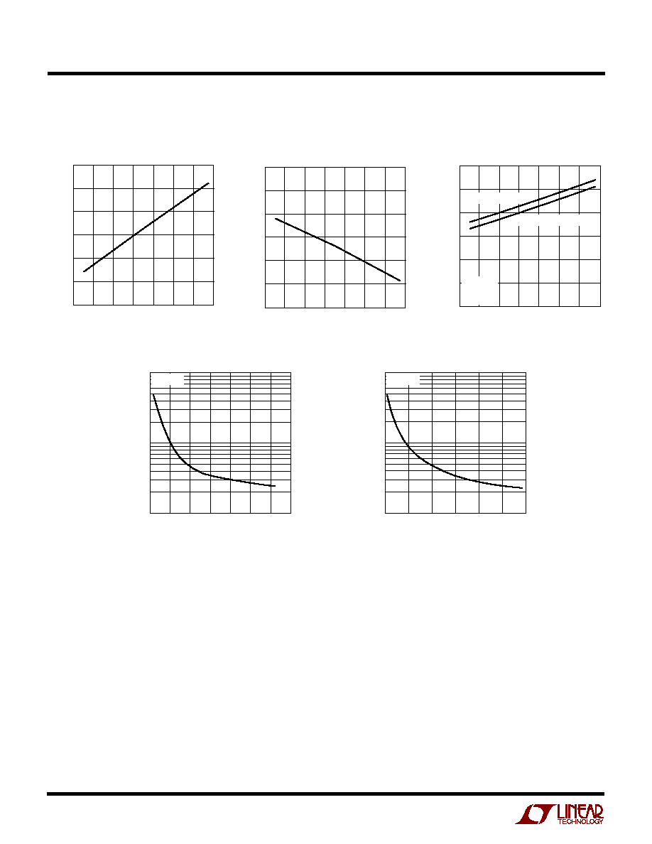
Undervoltage Response Time
Overvoltage Response Time
Fuse Window Positive Threshold
vs Temperature
Fuse Window Negative Threshold
vs Temperature
Output R
DS(ON)
vs Temperature
TEMPERATURE (
°
C)
FUSE POSITIVE THRESHOLD (V)
1921 G07
2.7
2.5
2.3
2.1
1.9
1.7
1.5
50
30
10
10
30
50
70
90
TEMPERATURE (
°
C)
FUSE NEGATIVE THRESHOLD (V)
1921 G08
2.0
2.2
2.4
2.6
2.8
3.0
3.2
50
30
10
10
30
50
70
90
SUPPLY STEP FROM UNDERVOLTAGE
RECOVERY THRESHOLD (V)
4.6
10000
4.8
1921 G10
RESPONSE TIME (
µ
s)
4.5
5.2
4.7
4.9
5.0
5.1
100
1000
T
A
= 25
°
C
SUPPLY STEP FROM OVERVOLTAGE
RECOVERY THRESHOLD (V)
1.5
10000
1.9
1921 G11
RESPONSE TIME (
µ
s)
1.3
2.5
1.7
2.1
2.3
100
1000
T
A
= 25
°
C
TYPICAL PERFOR A CE CHARACTERISTICS
U
W
TEMPERATURE (
°
C)
50
OUTPUT R
DS(ON)
(
)
20
25
30
10
50
1921 G09
15
10
30
10
30
70
90
5
0
OUT A (OUT F = 0V)
OUT F, OUT B (OUT A = 0V)
V
A
= 35V
V
B
= 35V
I = 10mA

LTC1921
5
1921f
V
A
(Pin 1): Supply to be Monitored. The voltage at this pin
is compared to the valid supply voltage window and the
result is output at OUT A (Pin 5). Supply current is drawn
from V
A
as well as from V
B
(Pin 8).
FUSE A (Pin 2): This pin monitors the state of a fuse by
comparing the voltage at this pin to the voltage at V
A
(Pin 1). The result is output at OUT F (Pin 4).
RTN (Pin 3): Supply Return Reference. This pin must be
at an equal or higher potential than the other pins and
should be wired to the 48V return.
OUT F (Pin 4): This pin indicates the state of the external
fuses by ORing the comparisons made to the FUSE A and
FUSE B pins. If V
FUSEA
V
A
(V
FUSEA
is within the specified
window around V
A
) and V
FUSEB
V
B
, then OUT F will
exhibit a high internal impedance to the RTN pin. If
V
FUSEA
V
A
or V
FUSEB
V
B
, then OUT F is shorted
internally to the RTN pin and can shunt enough current to
turn off an optoisolator or LED wired between these pins.
OUT F should be clamped externally so that it cannot be
driven more than 8V below RTN. This is done automati-
cally by the optoisolator or LED diodes shown in the
application circuits.
OUT A (Pin 5): Indicates the state of V
A
. If V
A
is within the
specified voltage window (neither undervoltage nor over-
voltage), OUT A will exhibit a high internal impedance to the
OUT F pin. If V
A
is outside the specified overvoltage or
undervoltage limits, then OUT A is shorted internally to the
OUT F pin and can shunt enough current to turn off an
optoisolator or LED wired between these pins. OUT A should
be clamped externally so that it cannot be driven more than
8V below RTN. This is done automatically by the
optoisolator or LED diodes shown in the application circuits.
OUT B (Pin 6): Indicates the state of V
B
. If V
B
is within the
specified voltage window (neither undervoltage nor over-
voltage), OUT B will exhibit a high internal impedance to the
OUT A pin. If V
B
is outside the specified overvoltage or
undervoltage limits, then OUT B is shorted internally to the
OUT A pin and can shunt enough current to turn off an
optoisolator or LED wired between these pins. OUT B should
be clamped externally so that it cannot be driven more than
8V below RTN. This is done automatically by the
optoisolator or LED diodes shown in the application circuits.
FUSE B (Pin 7): This pin monitors the state of a fuse by
comparing the voltage at this pin to the voltage at V
B
(Pin 8). The result is output at OUT F (Pin 4).
V
B
(Pin 8): Supply to be Monitored. The voltage at this pin
is compared to the valid supply voltage window and the
result is output at OUT B (Pin 6). Supply current is drawn
from V
B
as well as from V
A
(Pin 1).
U
U
U
PI FU CTIO S