 | ÐлекÑÑоннÑй компоненÑ: LTC1922-1 | СкаÑаÑÑ:  PDF PDF  ZIP ZIP |
Äîêóìåíòàöèÿ è îïèñàíèÿ www.docs.chipfind.ru
LTC3722-1/LTC3722-2
1
372212i
Information furnished by Linear Technology Corporation is believed to be accurate and reliable.
However, no responsibility is assumed for its use. Linear Technology Corporation makes no represen-
tation that the interconnection of its circuits as described herein will not infringe on existing patent rights.
Final Electrical Specifications
s
Adaptive or Manual Delay Control for Zero Voltage
Switching Operation
s
Adjustable Synchronous Rectification Timing for
Highest Efficiency
s
Adjustable Maximum ZVS Delay
s
Adjustable System Undervoltage Lockout and
Hysteresis
s
Programmable Leading Edge Blanking
s
Very Low Start-Up and Quiescent Currents
s
Current Mode (LTC3722-1) or Voltage Mode
(LTC3722-2) Operation
s
Programmable Slope Compensation
s
V
CC
UVLO and 25mA Shunt Regulator
s
50mA Output Drivers
s
Soft-Start, Cycle-by-Cycle Current Limiting and
Hiccup Mode Short-Circuit Protection
s
5V, 15mA Low Dropout Regulator
APPLICATIO S
U
FEATURES
DESCRIPTIO
U
Synchronous Dual Mode
Phase Modulated
Full Bridge Controllers
February 2003
The LTC
®
3722-1/LTC3722-2 phase shift PWM controllers
provide all of the control and protection functions neces-
sary to implement a high efficiency, zero voltage switched
(ZVS), full bridge power converter. Adaptive ZVS circuitry
delays the turn-on signals for each MOSFET independent
of internal and external component tolerances. Manual
delay set mode enables secondary side control operation
or direct control of switch turn-on delays.
The LTC3722-1/LTC3722-2 feature adjustable synchro-
nous rectifier timing for optimal efficiency. A UVLO pro-
gram input provides accurate system turn-on and turn-off
voltages. The LTC3722-1 features peak current mode
control with programmable slope compensation and lead-
ing edge blanking, while the LTC3722-2 employs voltage
mode control with voltage feedforward capability.
The LTC3722-1/LTC3722-2 feature extremely low operat-
ing and start-up currents. Both devices include a full range
of protection features and are available in the 24-pin
surface mount (GN) package.
, LTC and LT are registered trademarks of Linear Technology Corporation.
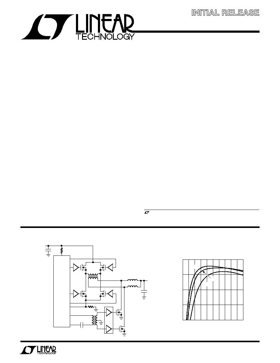
C
IN
R1
LTC3722
V
IN
36V TO 72V
MA
ME
MF
MB
MC
MD
1/2
U1
1/2
U1
U2
L1
L2
RCS
T1
T2
C1
V
OUT
12V
C
OUT
3722 · TA01A
U1, U2: LTC1693-1 DUAL GATE DRIVER
s
Telecommunications, Infrastructure Power Systems
s
Distributed Power Architectures
s
Server Power Supplies
12V
OUT
, 240W Converter Efficiency
TYPICAL APPLICATIO
U
CURRENT (A)
0
EFFICIENCY (%)
95
90
85
80
75
16
3722 TA01b
4
2
6
10
14
18
8
12
20
36V
IN
72V
IN
48V
IN

LTC3722-1/LTC3722-2
2
372212i
V
CC
to GND (Low Impedance Source) ......... 0.3 to 10V
(Chip Self Regulates at 10.3V)
UVLO to GND ................................................ 0.3 to V
CC
All Other Pins to GND
(Low Impedance Source) ....................... 0.3 to 5.5V
V
CC
(Current Fed) ................................................. 25mA
ABSOLUTE AXI U
RATI GS
W
W
W
U
PACKAGE/ORDER I FOR ATIO
U
U
W
(Note 1)
V
REF
Output Current ................................ Self Regulated
Outputs (A,B,C,D,E,F) Current ..........................
±
100mA
Operating Temperature Range (Note 6)
LTC3722E ........................................... 40
°
C to 85
°
C
Storage Temperature Range ................. 65
°
C to 150
°
C
Lead Temperature (Soldering, 10 sec).................. 300
°
C
ORDER PART
NUMBER
LTC3722EGN-1
T
JMAX
= 125
°
C,
JA
= 100
°
C/W
1
2
3
4
5
6
7
8
9
10
11
12
TOP VIEW
GN PACKAGE
24-LEAD NARROW PLASTIC SSOP
24
23
22
21
20
19
18
17
16
15
14
13
SYNC
DPRG
CS
COMP
RLEB
FB
SS
NC
PDLY
SBUS
ADLY
UVLO
C
T
GND
PGND
OUTA
OUTB
OUTC
V
CC
OUTD
OUTE
OUTF
V
REF
SPRG
Consult LTC Marketing for parts specified with wider operating temperature ranges.
ORDER PART
NUMBER
LTC3722EGN-2
T
JMAX
= 125
°
C,
JA
= 100
°
C/W
1
2
3
4
5
6
7
8
9
10
11
12
TOP VIEW
GN PACKAGE
24-LEAD NARROW PLASTIC SSOP
24
23
22
21
20
19
18
17
16
15
14
13
SYNC
RAMP
CS
COMP
DPRG
FB
SS
NC
PDLY
SBUS
ADLY
UVLO
C
T
GND
PGND
OUTA
OUTB
OUTC
V
CC
OUTD
OUTE
OUTF
V
REF
SPRG
LTC3722-1/LTC3722-2
3
372212i
ELECTRICAL CHARACTERISTICS
The
q
denotes the specifications which apply over the full operating
temperature range, otherwise specifications are at T
A
= 25
°
C. V
CC
= 9.5V, C
T
= 270pF, R
DPRG
= 60.4k, R
SPRG
= 100k, T
A
= t
MIN
to t
MAX
,
unless otherwise noted.
SYMBOL
PARAMETER
CONDITIONS
MIN
TYP
MAX
UNITS
Input Supply
V
CCUV
V
CC
Under Voltage Lockout
Measured on V
CC
10.25
10.5
V
V
CCHY
V
CC
UVLO Hysteresis
Measured on V
CC
3.8
4.2
V
I
CCST
Start-Up Current
V
CC
= V
UVLO
0.3V
q
145
230
µ
A
I
CCRN
Operating Current
No Load on Outputs
5
8
mA
V
SHUNT
Shunt Regulator Voltage
Current into V
CC
= 10mA
10.3
10.8
V
R
SHUNT
Shunt Resistance
Current into V
CC
= 10mA to 17mA
1.1
3.5
SUVLO
System UVLO Threshold
Measured on UVLO Pin, 7mA into V
CC
4.8
5.0
5.2
V
SHYST
System UVLO Hysteresis Current
Current Flows Out of UVLO Pin, 7mA into V
CC
8.5
10
11.5
µ
A
Delay Blocks
DTHR
Delay Pin Threshold
SBUS = 1.5V
q
1.4
1.5
1.6
V
ADLY and PDLY
SBUS = 2.25V
q
2.1
2.25
2.4
V
DHYS
Delay Hysteresis Current
SBUS = 1.5V, ADLY/PDLY = 1.7V
1.3
mA
ADLY and PDLY
DTMO
Delay Timeout
R
DPRG
= 60.4K
100
ns
DFXT
Fixed Delay Threshold
Measured on SBUS
4
V
DFTM
Fixed Delay Time
ADLY,PDLY = 1V, SBUS = V
REF
70
ns
Phase Modulator
I
RMP
Ramp Discharge Current
RAMP = 1V, COMP = 0V, C
T
= 4V,
50
mA
LTC3722-1 Only
I
SLP
Slope Compensation Current
Measured on CS, C
T
= 1V
30
µ
A
C
T
= 2.25V
68
µ
A
DC
MAX
Maximum Phase Shift
COMP = 4.5V
q
95
98.5
%
DC
MIN
Minimum Phase Shift
COMP = 0V
q
0
0.5
%
Oscillator
OSCI
Initial Accuracy
T
A
= 25
°
C, C
T
= 270pF
225
250
275
kHz
OSCT
Total Variation
V
CC
= 6.5V to 9.5V
q
215
250
285
kHz
OSCV
C
T
Ramp Amplitude
Measured on C
T
2.2
V
OSYT
SYNC Threshold
Measured on SYNC
1.6
1.9
2.2
V
OSYW
Minimum SYNC Pulse Width
Measured at Outputs (Note 2)
100
ns
OSYR
SYNC Frequency Range
Measured at Outputs (Note 2)
1000
kHz

LTC3722-1/LTC3722-2
4
372212i
ELECTRICAL CHARACTERISTICS
The
q
denotes the specifications which apply over the full operating
temperature range, otherwise specifications are at T
A
= 25
°
C. V
CC
= 9.5V, T
A
= t
MIN
to t
MAX
, unless otherwise noted.
SYMBOL
PARAMETER
CONDITIONS
MIN
TYP
MAX
UNITS
Error Amplifier
V
FB
FB Input Voltage
COMP = 2.5V (Note 4)
1.172
1.204
1.236
V
FBI
FB Input Range
Measured on FB (Note 5)
0.3
2.5
V
A
VOL
Open-Loop Gain
COMP = 1V to 3V (Note 4)
70
90
dB
IIB
Input Bias Current
COMP = 2.5V (Note 4)
5
20
nA
V
OH
Output High
Load on COMP = 100
µ
A
4.7
4.92
V
V
OL
Output Low
Load on COMP = 100
µ
A
0.18
0.4
V
I
SOURCE
Output Source Current
COMP = 2.5V
400
800
µ
A
I
SINK
Output Sink Current
COMP = 2.5V
2
5
mA
Reference
V
REF
Initial Accuracy
T
A
= 25
°
C, Measured on V
REF
4.925
5.00
5.075
V
REFLD
Load Regulation
Load on V
REF
= 100
µ
A to 5mA
2
15
mV
REFLN
Line Regulation
V
CC
= 6.5V to 9.5V
0.9
10
mV
REFTV
Total Variation
Line, Load
q
4.900
5.000
5.100
V
REFSC
Short-Circuit Current
V
REF
Shorted to GND
18
30
45
mA
Outputs
OUTH(x)
Output High Voltage
I
OUT(x)
= 50mA
7.9
8.4
V
OUTL(x)
Output Low Voltage
I
OUT(x)
= 50mA
0.6
1
V
R
HI(x)
Pull-Up Resistance
I
OUT(x)
= 50mA to 10mA
22
30
R
LO(x)
Pull-Down Resistance
I
OUT(x)
= 50mA to 10mA
12
20
t
r(x)
Rise Time
C
OUT(x)
= 50pF
5
15
ns
t
f(x)
Fall Time
C
OUT(x)
= 50pF
5
15
ns
SDEL
SYNC Driver Turn-0ff Delay
R
SPRG
= 100k
180
ns
Current Limit and Shutdown
CLPP
Pulse by Pulse Current Limit Threshold
Measured on CS
240
270
300
mV
CLSD
Shutdown Current Limit Threshold
Measured on CS
0.55
0.65
0.73
V
CLDEL
Current Limit Delay to Output
100mV Overdrive on CS (Notes 3, 7)
80
ns
SSI
Soft-Start Current
SS = 2.5V
7
12
17
µ
A
SSR
Soft-Start Reset Threshold
Measured on SS
0.7
0.4
0.1
V
FLT
Fault Reset Threshold
Measured on SS
4.5
3.9
3.5
V
Note 1: Absolute Maximum Ratings are those values beyond which the life
of a device may be impaired.
Note 2: Sync amplitude = 5V
P-P
, pulse width = 50ns. Verify output (A-F)
frequency = 1/2 sync frequency.
Note 3: Includes leading edge blanking delay, R
LEB
= 20k.
Note 4: FB is driven by a servo-loop amplifier to control V
COMP
for these
tests.
Note 5: Set FB to 0.3V, 2.5V and insure that COMP does not phase
invert.
Note 6: The LTC3722E-1/LTC3722E-2 are guaranteed to meet
performance specifications from 0
°
C to 85
°
C. Specifications over the
40
°
C to 85
°
C operating temperature range are assured by design,
characterization and correlation with statistical process controls.
Note 7: Guaranteed by design, not tested in production.

LTC3722-1/LTC3722-2
5
372212i
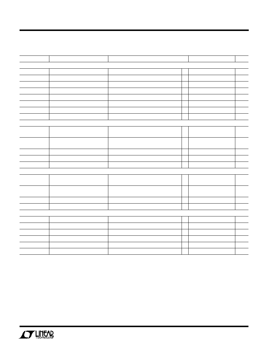
Start-Up I
CC
vs V
CC
V
CC
vs I
SHUNT
Oscillator Frequency vs
Temperature
Leading Edge Blanking Time
vs R
LEB
V
REF
vs I
REF
V
REF
vs Temperature
Error Amplifier Gain/Phase
TYPICAL PERFOR A CE CHARACTERISTICS
U
W
V
CC
(V)
0
I
CC
(
µ
A)
100
150
8
3722 · G01
50
0
2
4
6
10
200
T
A
= 25
°
C
I
SHUNT
(mA)
0
V
CC
(V) 10.00
10.25
40
3722 · G02
9.75
9.50
10
20
30
50
10.50
T
A
= 25
°
C
TEMPERATURE (
°
C)
FREQUENCY (kHz)
240
250
80
3722 · G03
230
220
40
60
20
20
0
40
60
100
260
C
T
= 270pF
R
LEB
(k
)
0
BLANK TIME (ns)
350
300
250
200
150
100
50
0
3722 · G04
40
100
20
10
30
50
70
90
60
80
T
A
= 25
°
C
I
REF
(mA)
0
V
REF
(V)
5.05
5.00
4.95
4.90
4.85
4.80
15
25
40
3722
· G05
5
10
20
30
35
T
J
= 25
°
C
T
J
= 85
°
C
T
J
= 40
°
C
TEMPERATURE (
°
C)
V
REF
(V)
4.99
5.00
80
3722 · G06
4.98
4.97
40
60
20
20
0
40
60
100
5.01
FREQUENCY (Hz)
GAIN (dB)
PHASE (DEG)
180
1M
3722 · G07
270
360
10
1k
100
10k
100k
10M
100
80
60
40
20
0
T
A
= 25
°
C