 | –≠–ª–µ–∫—Ç—Ä–æ–Ω–Ω—ã–π –∫–æ–º–ø–æ–Ω–µ–Ω—Ç: LTC1928-5 | –°–∫–∞—á–∞—Ç—å:  PDF PDF  ZIP ZIP |
ƒÓÍÛÏÂÌÚýˆËˇ Ë ÓÔËÒýÌˡ www.docs.chipfind.ru

1
LTC1928-5
, LTC and LT are registered trademarks of Linear Technology Corporation
ThinSOT is a trademark of Linear Technology Corporation.
FEATURES
APPLICATIO S
U
DESCRIPTIO
U
TYPICAL APPLICATIO
N
U
s
Low Output Noise: 90
µ
V
RMS
(100kHz BW)
s
Fixed Output Voltage: 5V
s
Input Voltage Range: 2.7V to 4.4V
s
No Inductors Required
s
Uses Small Ceramic Capacitors
s
Output Current Up to 30mA
s
550kHz Switching Frequency
s
Low Operating Current: 190
µ
A
s
Low Shutdown Current: 4
µ
A
s
Internal Thermal Shutdown and Current Limiting
s
Low Profile (1mm) ThinSOT
TM
Package
The LTC
Æ
1928-5 is a doubler charge pump with an internal
low noise, low dropout (LDO) linear regulator. The part is
designed to provide a low noise boosted supply voltage for
powering noise sensitive devices such as high frequency
VCOs in wireless applications.
An internal charge pump converts a 2.7V to 4.4V input to
a boosted output, while the internal LDO regulator con-
verts the boosted voltage to a low noise regulated output.
The regulator is capable of supplying up to 30mA of output
current. Shutdown reduces the supply current to < 8
µ
A,
removes the load from V
IN
by disabling the regulator and
discharges V
OUT
to ground through a 200
switch.
The LTC1928-5 LDO regulator is stable with only 2
µ
F on
the output. Small ceramic capacitors can be used, reduc-
ing PC board area.
The LTC1928-5 is short-circuit and overtemperature pro-
tected. The part is available in a 6-pin low profile
(1mm)ThinSOT package.
s
VCO Power Supplies for Cellular Phones
s
2-Way Pagers
s
Wireless PCMCIA Cards
s
Portable Medical Instruments
s
Low Power Data Acquisition
s
Remote Transmitters
s
White LED Drivers
s
GaAs Switches
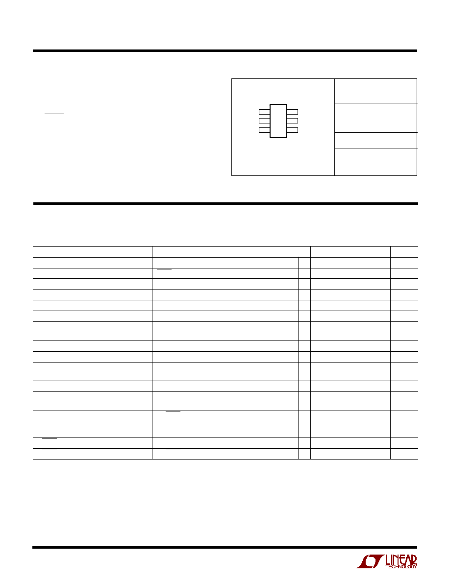
Figure 1. Low Noise 5V Power Supply
Doubler Charge Pump with
Low Noise Linear Regulator
in ThinSOT
Output Noise (BW = 10Hz to 2.5MHz)
V
OUT
200
µ
V/DIV
C
CPO
= C
OUT
= 4.7
µ
F
100
µ
s/DIV
19285 TA01
I
OUT
= 10mA
V
IN
= 3V
V
OUT
= 5V
T
A
= 25
∞
C
1
5
6
3
4
2
V
OUT
CPO
GND
V
IN
2.7V TO 4.4V
V
IN
CP
CN/SHDN
5V
4.7
µ
F
0.47
µ
F
4.7
µ
F
4.7
µ
F
19285 F01
V
OUT
LTC1928-5
2
LTC1928-5
T
JMAX
= 125
∞
C,
JA
= 230
∞
C/ W
ORDER PART
NUMBER
V
IN
to Ground .............................................. ≠ 0.3V to 5V
V
OUT
Voltage ........................................... ≠ 0.3V to 5.25V
CPO to Ground ........................................................ 10V
CN/SHDN to Ground ..................... ≠ 0.3V to (V
IN
+ 0.3V)
V
OUT
Short-Circuit Duration ............................. Indefinite
I
OUT .........................................................................................
40mA
Operating Temperature Range (Note 2) ...≠40
∞
C to 85
∞
C
Maximum Junction Temperature ......................... 125
∞
C
Storage Temperature Range ................. ≠ 65
∞
C to 150
∞
C
Lead Temperature (Soldering, 10 sec).................. 300
∞
C
(Note 1)
Consult factory for parts specified with wider operating temperature ranges.
1
2
3
V
IN
GND
V
OUT
6
5
4
CN/SHDN
CP
CPO
TOP VIEW
S6 PACKAGE
6-LEAD PLASTIC SOT-23
S6 PART MARKING
LTKT
PARAMETER
CONDITIONS
MIN
TYP
MAX
UNITS
V
IN
Operating Voltage
q
2.7
4.4
V
I
VIN
Shutdown Current
SHDN = 0V (Note 5)
q
4
8
µ
A
I
VIN
Operating Current
I
OUT
= 0mA, Burst Mode
TM
Operation
q
190
330
µ
A
Regulated Output Voltage
I
OUT
= 1mA
q
4.9
5
5.1
V
V
OUT
Temperature Coefficient
±
50
ppm
Charge Pump Oscillator Frequency
I
OUT
> 500
µ
A, V
IN
= 2.7V to 4.4V
q
480
550
620
kHz
CPO Output Resistance
V
IN
= 2.7V, I
OUT
= 10mA
q
17
30
V
IN
= 4.4V, I
OUT
= 10mA
q
14
24
V
OUT
Dropout Voltage (Note 3)
I
OUT
= 10mA, V
OUT
= 5V
q
100
mV
V
OUT
Enable Time
R
LOAD
= 2k
0.6
ms
V
OUT
Output Noise Voltage
I
OUT
= 10mA, 10Hz
f
100kHz
90
µ
V
RMS
I
OUT
= 10mA, 10Hz
f
2.5MHz
800
µ
V
P-P
V
OUT
Line Regulation
V
IN
= 2.7V to 4.4V, I
OUT
= 0
q
4
20
mV
V
OUT
Load Regulation
I
OUT
= 1mA to 10mA
q
2
10
mV
I
OUT
= 1mA to 30mA (Note 4)
4
mV
V
OUT
Shutdown Resistance
CN/SHDN = 0V (Note 5)
V
IN
= 2.7V, Resistance Measured to Ground
q
160
400
V
IN
= 4.4V, Resistance Measured to Ground
q
100
300
CN/SHDN Input Threshold
V
IN
= 2.7V to 4.4V (Note 5)
q
0.15
0.5
1.6
V
CN/SHDN Input Current
CN/SHDN = 0V (Note 5)
q
≠ 1
≠ 3
≠ 6
µ
A
Burst Mode is a trademark of Linear Technology Corporation.
LTC1928ES6-5
ABSOLUTE AXI U RATI GS
W
W
W
U
PACKAGE/ORDER I FOR ATIO
U
U
W
ELECTRICAL CHARACTERISTICS
Note 1: Absolute Maximum Ratings are those values beyond which the life
of a device may be impaired.
Note 2: The LTC1928ES6-5 is guaranteed to meet performance
specifications from 0
∞
C to 70
∞
C. Specifications over the ≠ 40
∞
C to 85
∞
C
operating temperature range are assured by design, characterization and
correlation with statistical process controls.
Note 3: Dropout voltage is the minimum input/output voltage required to
maintain regulation at the specified output current. In dropout the output
voltage will be equal to: V
CPO
≠ V
DROPOUT
(see Figure 2).
The
q
denotes specifications which apply over the full operating temperature range, otherwise specifications are T
A
= 25
∞
C.
V
IN
= 3V, C
FLY
= 0.47
µ
F, C
OUT
, C
CPO
, C
IN
= 4.7
µ
F unless otherwise specified.
3
LTC1928-5
Note 5: CN/SHDN must be driven with a source impedance of at least
100
(R
SOURCE
) to prevent damage to the part. This pin is multiplexed
and may be connected through a low switch impedance to V
IN
. There may
be a large amount of current (V
IN
/R
SOURCE
) until the shutdown state
occurs after which the charge pump switches at CN/SHDN become high
impedance and the current will fall to < 8
µ
A.
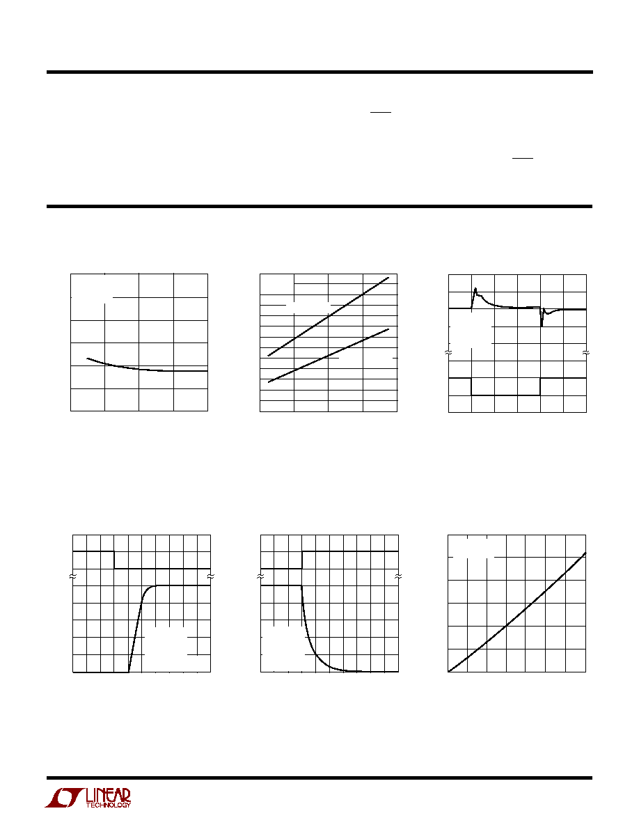
CPO Output Resistance vs V
IN
Min and Max V
CPO
vs V
IN
V
OUT
Transient Response
Note 4: Operating conditions are limited by maximum junction
temperature. The regulated output specification will not apply for all
possible combinations of input voltage and output current. When
operating at maximum input voltage, the output current range may be
limited. When operating at maximum output current, the input voltage
range may be limited.
Shutdown to Enable Timing
(Figure 5)
Enable to Shutdown Timing
(Figure 5)
V
IN
(V)
R
CPO
(
)
35
30
25
20
15
10
5
2.5
3.0
3.5
19285 G01
4.0
4.5
T
A
= 25
∞
C
C
FLY
= 0.47
µ
F
I
OUT
= 10mA
V
IN
(V)
V
CPO
(V)
9
8
7
6
5
4
3
2.5
3.0
3.5
19285 G02
4.0
4.5
(A)
(A) THE MAXIMUM GENERATED NO LOAD
CPO VOLTAGE
(B) THE MINIMUM ALLOWABLE CPO VOLTAGE,
AT FULL LOAD, TO ENSURE THAT THE LDO
IS NOT DISABLED
(B)
V
CPO
= 1.45(V
IN
)
V
CPO
= 2(V
IN
)
T
A
= 25
∞
C
TIME (
µ
s)
0
50
V
OUT
(mV)
I
OUT
(mA)
100
200
150
250
300
19285 G03
10
5
0
≠5
≠10
15
10
5
0
T
A
= 25
∞
C
V
IN
= 3V
V
OUT
= 5V
C
OUT
= 4.7
µ
F
200
µ
s/DIV
SHDN (V)
V
OUT
(V)
2
0
5
4
3
2
1
0
19285 G04
T
A
= 25
∞
C
V
IN
= 3V
V
OUT
= 5V
I
OUT
= 10mA
C
OUT
= C
CPO
= 4.7
µ
F
1ms/DIV
SHDN (V)
V
OUT
(V)
2
0
5
4
3
2
1
0
19285 G05
NO LOAD
T
A
= 25
∞
C
V
IN
= 3V
V
OUT
= 5V
C
OUT
= 4.7
µ
F
ELECTRICAL CHARACTERISTICS
V
OUT
Voltage vs Temperature
TEMPERATURE (
∞
C)
≠50
5.040
5.030
5.020
5.010
5.000
4.990
4.980
25
75
19285 G06
≠25
0
50
100
125
V
OUT
VOLTAGE (V)
V
IN
= 3V
I
OUT
= 10mA
TYPICAL PERFOR A CE CHARACTERISTICS
U
W

4
LTC1928-5
Operating Current vs V
IN
(No Load)
BLOCK DIAGRA
W
≠
+
≠
+
CHARGE PUMP
AND
SLEW CONTROL
5
1
6
2
3
4
CN/SHDN
CP
CLK B
ENB
CPO
V
OUT
V
IN
C
FLY
0.47
µ
F
C
CPO
4.7
µ
F
C
OUT
4.7
µ
F
POR/
SHDN
CONTROL
550kHz
OSCILLATOR
SD
BURST
V
REF
= 1.235V
≠
+
C
IN
4.7
µ
F
SD
GND
19285 BD
160
V
IN
(V)
OPERATING CURRENT (
µ
A)
260
240
220
200
180
160
140
120
100
19285 G07
2.5
3.0
3.5
4.0
4.5
T
A
= 25
∞
C
Efficiency vs Supply Voltage
SUPPLY VOLTAGE (V)
2.6
40
EFFICIENCY (%)
50
70
80
90
3.0
3.4 3.6
4.4
19285 G08
60
2.8
3.2
3.8 4.0 4.2
100
T
A
= 25
∞
C
I
OUT
= 15mA
C
FLY
= 0.47
µ
F
Output Voltage vs Output Current
OUTPUT CURRENT (mA)
0
OUTPUT VOLTAGE (V)
35
40
19285 G09
5
10
15
20
25
30
4.901
4.900
4.989
4.988
4.987
4.986
4.985
4.984
4.983
4.982
T
A
= 25
∞
C
V
IN
= 3V
C
FLY
= 0.47
µ
F
TYPICAL PERFOR A CE CHARACTERISTICS
U
W
5
LTC1928-5
V
IN
(Pin 1): Input Voltage, 2.7V to 4.4V. V
IN
should be
bypassed with a
2
µ
F low ESR capacitor as close to the
pin as possible for best performance. A minimum capaci-
tance value of 0.1
µ
F is required.
GND (Pin 2): System Ground.
V
OUT
(Pin 3): Low Noise Regulated Output Voltage. V
OUT
should be bypassed with a
2
µ
F low ESR capacitor as
close to the pin as possible for best performance. The V
OUT
voltage is internally set to 5V.
PI
N
FU
N
CTIO
N
S
U
U
U
CPO (Pin 4): Boosted Unregulated Voltage. Approxi-
mately 1.95V
IN
at low loads. Bypass with a
2
µ
F low ESR
capacitor.
CP (Pin 5): Flying Capacitor Positive Input.
CN/SHDN (Pin 6): Flying Capacitor Negative Input and
SHDN. When this pin is pulled to ground through a 100
resistor, the part will go into shutdown within approxi-
mately 30
µ
s.
Operation
The LTC1928-5 uses a switched-capacitor charge pump
to generate a CPO voltage of approximately 2V
IN
. CPO
powers an internal low dropout linear regulator that sup-
plies a regulated output at V
OUT
. Internal comparators are
used to sense CPO and V
IN
voltages for power-up condi-
tioning. The output current is sensed to determine the
charge pump operating mode. A trimmed internal bandgap
is used as the voltage reference and a trimmed internal
oscillator is used to control the charge pump switches.
The charge pump is a doubler configuration that uses one
external flying capacitor. When enabled, a 2-phase
nonoverlapping clock controls the charge pump switches.
At start-up, the LDO is disabled and the load is removed
from CPO. When CPO reaches 1.75V
IN
the LDO is enabled.
If CPO falls below 1.45V
IN
the LDO will be disabled. Gen-
erally, the charge pump runs open loop with continuous
clocking for low noise. If CPO is greater than 1.95V
IN
and
I
OUT
is less than 200
µ
A, the charge pump will operate in
Burst Mode operation for increased efficiency but slightly
higher output noise. In Burst Mode operation, the clock is
disabled when CPO reaches 1.95V
IN
and enabled when
CPO droops by about 150mV. The switching frequency is
precisely controlled to ensure that the frequency is above
455kHz and at the optimum rate to ensure maximum effi-
ciency. The switch edge rates are also controlled to mini-
mize noise. The effective output resistance at CPO is
dependent on the voltage at V
IN
, CPO, the flying capacitor
value C
FLY
and the junction temperature. A low ESR ca-
pacitor of
2
µ
F should be used at CPO for minimum noise.
APPLICATIO
N
S I
N
FOR
M
ATIO
N
W
U
U
U
The LDO is used to filter the ripple on CPO and to set an
output voltage independent of CPO. V
OUT
is set by an
internal reference and resistor divider. The LDO requires a
capacitor on V
OUT
for stability and improved load transient
response. A low ESR capacitor of
2
µ
F should be used.
Maximum I
OUT
Calculations
The maximum available current can be calculated based
on the open circuit CPO voltage, the dropout voltage of the
LDO and the effective output resistance of the charge
pump. The open circuit CPO voltage is approximately 2V
IN
(see Figure 2).
Example:
V
IN
= 3V
V
OUT
= 5V
R
CPO
= 30
Maximum unloaded CPO voltage = 2V
IN
= 6V
V
DROPOUT(MAX)
= 100mV
I
OUT(MAX)
= (2V
IN
≠ V
DROPOUT(MAX)
≠ V
OUT
)/R
CPO
= (6V ≠ 0.1V ≠ 5V)/30
= 30mA
V
CPO
must be greater than 1.45V
IN
= 4.35V. To confirm
this, calculate V
CPO
:
V
CPO
= 6V ≠ (30mA ∑ 30
) = 5.1V
For minimum noise applications the LDO must be kept out
of dropout to prevent CPO noise from coupling into V
OUT
.