 | ÐлекÑÑоннÑй компоненÑ: LTC1929IG | СкаÑаÑÑ:  PDF PDF  ZIP ZIP |
Äîêóìåíòàöèÿ è îïèñàíèÿ www.docs.chipfind.ru

1
LTC1929
2-Phase, High Efficiency,
Synchronous Step-Down
Switching Regulator
August 1999
, LTC and LT are registered trademarks of Linear Technology Corporation.
OPTI-LOOP is a trademark of Linear Technology Corporation.
The LTC
®
1929 is a 2-phase, single output, synchronous
step-down current mode switching regulator controller
that drives N-channel external power MOSFET stages in a
phase-lockable fixed frequency architecture. The 2-phase
controller drives its two output stages out of phase at
frequencies up to 300kHz to minimize the RMS ripple
currents in both input and output capacitors. The 2-phase
technique effectively multiplies the fundamental frequency
by two, improving transient response while operating
each channel at an optimum frequency for efficiency.
Thermal design is also simplified.
An internal differential amplifier provides true remote
sensing of the regulated supply's positive and negative
output terminals as required by high current applications.
The RUN/SS pin provides soft-start and a defeatable,
timed, latched short-circuit shutdown to shut down both
channels. Internal foldback current limit provides protec-
tion for the external sychronous MOSFETs in the event of
an output fault. OPTI-LOOP compensation allows the
transient response to be optimized over a wide range of
output capacitance and ESR values.
APPLICATIO S
U
FEATURES
DESCRIPTIO
U
TYPICAL APPLICATIO
U
Figure 1. High Current 2-Phase Step-Down Converter
s
Desktop Computers
s
Internet/Network Servers
s
Large Memory Arrays
s
DC Power Distribution Systems
s
2-Phase Single Output Controller
s
Reduces Required Input Capacitance and Power
Supply Induced Noise
s
Current Mode Control Ensures Current Sharing
s
Phase-Lockable Fixed Frequency: 150kHz to 300kHz
s
True Remote Sensing Differential Amplifier
s
OPTI-LOOP
TM
Compensation Improves Transient
Response
s
±
1% Output Voltage Accuracy
s
Wide V
IN
Range: 4V to 36V Operation
s
Very Low Dropout Operation: 99% Duty Cycle
s
Adjustable Soft-Start Current Ramping
s
Internal Current Foldback
s
Short-Circuit Shutdown Timer with Defeat Option
s
Overvoltage Soft-Latch Eliminates Nuisance Trips
s
Available in 28-Lead SSOP Package
1929 TA01
TG1
BOOST1
SW1
BG1
PGND
SENSE1
+
SENSE1
TG2
BOOST2
SW2
BG2
INTV
CC
SENSE2
+
SENSE2
V
IN
RUN/SS
EAIN
I
TH
V
DIFFOUT
V
OS
V
OS
+
LTC1929
SGND
S
0.1
µ
F
0.1
µ
F
8.06k
1000pF
S
S
S
S
S
S
S
S
S
10
10k
8.06k
+
10
µ
F
×
4
35V
CERAMIC
+
C
OUT
1000
µ
F
×
2
4V
V
OUT
1.6V/40A
L1
1
µ
H
0.002
V
IN
5V TO 28V
L2
1
µ
H
D2
D1
0.47
µ
F
S
0.47
µ
F
100pF
10
µ
F
0.002
C
OUT
: T510E108K004AS
L1, L2: CEPH149-1ROMC
Final Electrical Specifications
Information furnished by Linear Technology Corporation is believed to be accurate and reliable.
However, no responsibility is assumed for its use. Linear Technology Corporation makes no represen-
tation that the interconnection of its circuits as described herein will not infringe on existing patent rights.
2
LTC1929
ORDER PART
NUMBER
LTC1929CG
LTC1929IG
ABSOLUTE AXI U
RATI GS
W
W
W
U
PACKAGE/ORDER I FOR ATIO
U
U
W
T
JMAX
= 125
°
C,
JA
= 95
°
C/W
Consult factory for Military grade parts.
ELECTRICAL CHARACTERISTICS
The
q
denotes the specifications which apply over the full operating
temperature range, otherwise specifications are at T
A
= 25
°
C. V
IN
= 15V, V
RUN/SS
= 5V unless otherwise noted.
(Note 1)
Input Supply Voltage (V
IN
).........................36V to 0.3V
Topside Driver Voltages (BOOST1,2) .........42V to 0.3V
Switch Voltage (SW1, 2) .............................36V to 5 V
SENSE1
+
, SENSE2
+
, SENSE1
,
SENSE2
Voltages ........................ (1.1)INTV
CC
to 0.3V
EAIN, V
OS
+
, V
OS
, EXTV
CC
, INTV
CC
,
RUN/SS, AMPMD Voltages .......................... 7V to 0.3V
Boosted Driver Voltage (BOOST-SW) .......... 7V to 0.3V
PLLFLTR, PLLIN, V
DIFFOUT
Voltages .... INTV
CC
to 0.3V
I
TH
Voltage ................................................2.7V to 0.3V
Peak Output Current <1
µ
s(TGL1,2, BG1,2) ................ 3A
INTV
CC
RMS Output Current ................................ 50mA
Operating Ambient Temperature Range
LTC1929C .................................................. 0
°
C to 85
°
C
LTC1929I .............................................. 40
°
C to 85
°
C
Junction Temperature (Note 2) ............................. 125
°
C
Storage Temperature Range ................. 65
°
C to 150
°
C
Lead Temperature (Soldering, 10 sec).................. 300
°
C
SYMBOL
PARAMETER
CONDITIONS
MIN
TYP
MAX
UNITS
Main Control Loop
V
EAIN
Regulated Feedback Voltage
(Note 3); I
TH
Voltage = 1.2V
q
0.792
0.800
0.808
V
V
SENSEMAX
Maximum Current Sense Threshold
V
SENSE
= 5V
65
75
85
mV
I
INEAIN
Feedback Current
(Note 3)
5
50
nA
V
LOADREG
Output Voltage Load Regulation
(Note 3)
Measured in Servo Loop; I
TH
Voltage = 0.7V
0.05
0.3
%
Measured in Servo Loop; I
TH
Voltage = 2V
0.1
0.5
%
V
REFLNREG
Reference Voltage Line Regulation
V
IN
= 3.6V to 30V (Note 3)
0.002
%/V
V
OVL
Output Overvoltage Threshold
Measured at V
EAIN
q
0.84
0.86
0.88
V
UVLO
Undervoltage Lockout
V
IN
Ramping Down
3
3.5
4
V
g
m
Transconductance Amplifier g
m
I
TH
= 1.2V; Sink/Source 5
µ
A; (Note 3)
3
mmho
g
mOL
Transconductance Amplifier Gain
I
TH
= 1.2V; (g
m
xZ
L
; No Ext Load); (Note 3)
1.5
V/mV
I
Q
Input DC Supply Current
(Note 4)
Normal Mode
EXTV
CC
Tied to V
OUT
; V
OUT
= 5V
470
µ
A
Shutdown
V
RUN/SS
= 0V
20
40
µ
A
I
RUN/SS
Soft-Start Charge Current
V
RUN/SS
= 1.9V
1.2
µ
A
V
RUN/SS
RUN/SS Pin ON Threshold
V
RUN/SS
Rising
1.0
1.5
1.9
V
V
RUN/SSLO
RUN/SS Pin Latchoff Arming
V
RUN/SS
Rising from 3V
4.1
V
I
SCL
RUN/SS Discharge Current
Soft Short Condition V
EAIN
= 0.5V;
0.5
2.0
4.0
µ
A
V
RUN/SS
= 4.5V
1
2
3
4
5
6
7
8
9
10
11
12
13
14
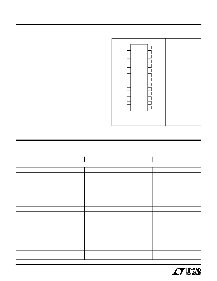
TOP VIEW
G PACKAGE
28-LEAD PLASTIC SSOP
28
27
26
25
24
23
22
21
20
19
18
17
16
15
RUN/SS
SENSE1
+
SENSE1
EAIN
PLLFLTR
PLLIN
NC
I
TH
SGND
V
DIFFOUT
V
OS
V
OS
+
SENSE2
SENSE2
+
NC
TG1
SW1
BOOST1
V
IN
BG1
EXTV
CC
INTV
CC
PGND
BG2
BOOST2
SW2
TG2
AMPMD

3
LTC1929
SYMBOL
PARAMETER
CONDITIONS
MIN
TYP
MAX
UNITS
ELECTRICAL CHARACTERISTICS
The
q
denotes the specifications which apply over the full operating
temperature range, otherwise specifications are at T
A
= 25
°
C. V
IN
= 15V, V
RUN/SS
= 5V unless otherwise noted.
I
SDLHO
Shutdown Latch Disable Current
V
EAIN
= 0.5V
1.6
5
µ
A
I
SENSE
Total Sense Pins Source Current
Each Channel: V
SENSE1
, 2
= V
SENSE1
+
, 2
+ = 0V
60
µ
A
DF
MAX
Maximum Duty Factor
In Dropout
98
99.5
%
Top Gate Transition Time:
TG1, 2 t
r
Rise Time
C
LOAD
= 3300pF
30
90
ns
TG1, 2 t
f
Fall Time
C
LOAD
= 3300pF
40
90
ns
Bottom Gate Transition Time:
BG1, 2 t
r
Rise Time
C
LOAD
= 3300pF
30
90
ns
BG1, 2 t
f
Fall Time
C
LOAD
= 3300pF
20
90
ns
TG/BG t
1D
Top Gate Off to Bottom Gate On Delay
Synchronous Switch-On Delay Time
C
LOAD
= 3300pF Each Driver
90
ns
BG/TG t
2D
Bottom Gate Off to Top Gate On Delay
Top Switch-On Delay Time
C
LOAD
= 3300pF Each Driver
90
ns
Internal V
CC
Regulator
V
INTVCC
Internal V
CC
Voltage
6V < V
IN
< 30V; V
EXTVCC
= 4V
4.8
5.0
5.2
V
V
LDO
INT
INTV
CC
Load Regulation
I
CC
= 0 to 20mA; V
EXTVCC
= 4V
0.2
1.0
%
V
LDO
EXT
EXTV
CC
Voltage Drop
I
CC
= 20mA; V
EXTVCC
= 5V
120
240
mV
V
EXTVCC
EXTV
CC
Switchover Voltage
I
CC
= 20mA, EXTV
CC
Ramping Positive
q
4.5
4.7
V
V
LDOHYS
EXTV
CC
Switchover Hysteresis
I
CC
= 20mA, EXTV
CC
Ramping Negative
0.2
V
Oscillator and Phase-Locked Loop
f
NOM
Nominal Frequency
V
PLLFLTR
= 1.2V
200
220
250
kHz
f
LOW
Lowest Frequency
V
PLLFLTR
= 0V
110
140
170
kHz
f
HIGH
Highest Frequency
V
PLLFLTR
2.4V
270
310
350
kHz
R
PLLIN
PLLIN
Input Resistance
50
k
I
PLLFLTR
Phase Detector Output Current
Sinking Capability
f
PLLIN
< f
OSC
15
µ
A
Sourcing Capability
f
PLLIN
> f
OSC
15
µ
A
R
RELPHS
Controller 2-Controller 1 Phase
180
Deg
Differential Amplifier/Op Amp Gain Block (Note 5)
A
DA
Gain
Differential Amp Mode
0.995
1
1.005
V/V
CMRR
DA
Common Mode Rejection Ratio
Differential Amp Mode; 0V < V
CM
< 5V
46
55
dB
R
IN
Input Resistance
Differential Amp Mode; Measured at V
OS
+ Input
80
k
V
OS
Input Offset Voltage
Op Amp Mode; V
CM
= 2.5V; V
DIFFOUT
= 5V;
6
mV
I
DIFFOUT
= 1mA
I
B
Input Bias Current
Op Amp Mode
30
200
nA
A
OL
Open Loop DC Gain
Op Amp Mode; 0.7V
V
DIFFOUT
< 10V
5000
V/mV
V
CM
Common Mode Input Voltage Range
Op Amp Mode
0
3
V
CMRR
OA
Common Mode Rejection Ratio
Op Amp Mode; 0V < V
CM
< 3V
70
90
dB
PSRR
OA
Power Supply Rejection Ratio
Op Amp Mode; 6V < V
IN
< 30V
70
90
dB
I
CL
Maximum Output Current
Op Amp Mode; V
DIFFOUT
= 0V
10
35
mA
V
O(MAX)
Maximum Output Voltage
Op Amp Mode; I
DIFFOUT
= 1mA
10
11
V
GBW
Gain-Bandwidth Product
Op Amp Mode; I
DIFFOUT
= 1mA
2
MHz
SR
Slew Rate
Op Amp Mode; R
L
= 2k
5
V/
µ
s

4
LTC1929
PI FU CTIO S
U
U
U
ELECTRICAL CHARACTERISTICS
Note 3: The LTC1929 is tested in a feedback loop that servos V
ITH
to a
specified voltage and measures the resultant V
EAIN
.
Note 4: Dynamic supply current is higher due to the gate charge being
delivered at the switching frequency. See Applications Information.
Note 5: When the AMPMD pin is high, the IC pins are connected directly to
the internal op amp inputs. When the AMPMD pin is low, internal MOSFET
switches connect four 40k resistors around the op amp to create a
standard unity-gain differential amp.
Note 1: Absolute Maximum Ratings are those values beyond which the
life of a device may be impaired.
Note 2: T
J
is calculated from the ambient temperature T
A
and power
dissipation P
D
according to the following formulas:
LTC1929CG: T
J
= T
A
+ (P
D
· 95
°
C/W)
RUN/SS (Pin 1): Combination of Soft-Start, Run Control
Input and Short-Circuit Detection Timer. A capacitor to
ground at this pin sets the ramp time to full current output.
Forcing this pin below 0.8V causes the IC to shut down all
internal circuitry. All functions are disabled in shutdown.
SENSE1
+
, SENSE2
+
(Pins 2,14): The (+) Input to the
Differential Current Comparators. The I
TH
pin voltage and
built-in offsets between SENSE
and SENSE
+
pins in
conjunction with R
SENSE
set the current trip threshold.
SENSE1
, SENSE2
(Pins 3, 13): The () Input to the
Differential Current Comparators.
EAIN (Pin 4): Input to the Error Amplifier that compares
the feedback voltage to the internal 0.8V reference voltage.
This pin is normally connected to a resistive divider from
the output of the differential amplifier (DIFFOUT).
PLLFLTR (Pin 5): The Phase-Locked Loop's Low Pass
Filter is tied to this pin. Alternatively, this pin can be driven
with an AC or DC voltage source to vary the frequency of
the internal oscillator.
PLLIN (Pin 6): External Synchronization Input to Phase
Detector. This pin is internally terminated to SGND with
50k
. The phase-locked loop will force the rising top gate
signal of controller 1 to be synchronized with the rising
edge of the PLLIN signal.
NC (Pins 7, 28): Not connected.
I
TH
(Pin 8): Error Amplifier Output and Switching Regula-
tor Compensation Point. Both current comparator's thresh-
olds increase with this control voltage. The normal voltage
range of this pin is from 0V to 2.4V
SGND (Pin 9): Signal Ground, common to both control-
lers, must be routed separately from the input switched
current ground path to the common () terminal(s) of the
C
OUT
capacitor(s).
V
DIFFOUT
(Pin 10): Output of a Differential Amplifier that
provides true remote output voltage sensing. This pin
normally drives an external resistive divider that sets the
output voltage.
V
OS
, V
OS
+
(Pins 11, 12): Inputs to an Operational Ampli-
fier. Internal precision resistors capable of being elec-
tronically switched in or out can configure it as a differen-
tial amplifier or an uncommitted Op Amp.
AMPMD (Pin 15): This Logic Input pin controls the
connections of internal precision resistors that configure
the operational amplifier as a unity-gain differential ampli-
fier.
TG2, TG1 (Pins 16, 27): High Current Gate Drives for Top
N-Channel MOSFETS. These are the outputs of floating
drivers with a voltage swing equal to INTV
CC
superim-
posed on the switch node voltage SW.
SW2, SW1 (Pins 17, 26): Switch Node Connections to
Inductors. Voltage swing at these pins is from a Schottky
diode (external) voltage drop below ground to V
IN
.
BOOST2, BOOST1 (Pins 18, 25): Bootstrapped Supplies
to the Topside Floating Drivers. Capacitors are connected
between the Boost and Switch pins, and Schottky diodes
are tied between the Boost and INTV
CC
pins.
BG2, BG1 (Pins 19, 23): Voltage Swing High Current Gate
Drives for Bottom Synchronous N-Channel MOSFETS.
Voltage swing at these pins is from ground to INTV
CC
.

5
LTC1929
PI FU CTIO S
U
U
U
FU CTIO AL DIAGRA
U
U
W
PGND (Pin 20): Driver Power Ground. Connects to sources
of bottom N-channel MOSFETS and the () terminals of
C
IN
.
INTV
CC
(Pin 21): Output of the Internal 5V Linear Low
Dropout Regulator and the EXTV
CC
Switch. The driver and
control circuits are powered from this voltage source.
Decouple to power ground with a 1
µ
F ceramic capacitor
placed directly adjacent to the IC and minimum of 4.7
µ
F
additional tantalum or other low ESR capacitor.
EXTV
CC
(Pin 22): External Power Input to an Internal
Switch . This switch closes and supplies INTV
CC,
bypass-
ing the internal
low dropout regulator whenever EXTV
CC
is
higher than 4.7V. See EXTV
CC
Connection in the Applica-
tions Information section. Do not exceed 7V on this pin
and ensure V
EXTVCC
V
INTVCC
.
V
IN
(Pin 24): Main Supply Pin. Should be closely decoupled
to the IC's signal ground pin.
SWITCH
LOGIC
0.8V
4.7V
5V
V
IN
V
IN
A1
CLK2
CLK1
+
+
+
V
REF
INTERNAL
SUPPLY
EXTV
CC
INTV
CC
SGND
+
5V
LDO
REG
SW
SHDN
TOP
BOOST
TG
C
B
C
IN
D
B
PGND
BOT
BG
INTV
CC
INTV
CC
V
IN
+
V
OUT
1929 FBD
R1
EAIN
DROP
OUT
DET
RUN
SOFT
START
BOT
FORCE BOT
S
R
Q
Q
OSCILLATOR
PLLLPF
50k
EA
0.86V
0.80V
OV
V
FB
1.2
µ
A
6V
V
IN
R2
+
R
C
4(V
FB
)
SHDN
RUN/SS
I
TH
C
C
C
SS
4(V
FB
)
SLOPE
COMP
+
SENSE
SENSE
+
INTV
CC
30k
45k
2.4V
45k
30k
I1
AMPMD
DIFFOUT
0V POSITION
PHASE DET
PLLIN
DUPLICATE FOR
SECOND CHANNEL
+
R
SENSE
L
C
OUT
+
V
OS
+
V
OS
F
IN
R
LP
C
LP