LTC1955
1
sn1955 1955fs
APPLICATIO S
U
FEATURES
DESCRIPTIO
U
TYPICAL APPLICATIO
U
The LTC
Æ
1955 provides all necessary supervisory and
power control functions for two smart cards, two S.A.M.
cards or a combination of S.A.M. and smart cards. It
provides a charge pump for battery powered applications
as well as all necessary level shifting circuitry.
The card voltages can be independently set to 1.8V, 3V or
5V. Both card interfaces include a card detection channel
with automatic debounce circuitry. To reduce wiring costs,
the LTC1955 interfaces to a microcontroller via a simple
4-wire serial interface. Multiple devices may be connected
in daisy-chain fashion so that the number of wires to the
card socket board is independent of the number of sock-
ets. Status data is returned over the same interface.
Extensive security features ensure proper deactivation
sequencing in the event of a supply fault or a smart card
electrical fault. The smart card pins can withstand greater
than 10kV ESD in-situ with no additional components.
The LTC1955 is available in a small 5mm
◊
5mm QFN
package.
s
Handheld Payment Terminals
s
Pay Telephones
s
ATM Machines
s
POS Terminals
s
Computer Keyboards
s
Multiple S.A.M. Sockets
, LTC and LT are registered trademarks of Linear Technology Corporation.
s
Compatible with ISO7816-3 and EMV Electrical
Specifications
s
Power Management and Control for Two Smart
Cards
s
Control/Status Serial Port May be Daisy-Chained
for Multicard Applications
s
Automatic Shutdown on Electrical Faults
s
Buck/Boost Charge Pump Generates 5V, 3V or 1.8V
Outputs (Smart Card Classes A, B and C)*
s
Independent 5V/3V/1.8V Level Control for Both Cards
s
Automatic Level Translation
s
Supervisory Functions Prevent Smart Card Faults
s
Low Operating Current: 250
µ
A Typical
s
Ultralow Shutdown Current
s
>10kV ESD on Smart Card Pins
s
Small 32-Pin 5mm
◊
5mm QFN Package
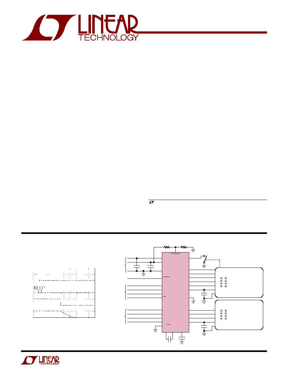
Dual Smart Card Interface
with Serial Control
4-WIRE
COMMAND
INTERFACE
4-WIRE
CARD
INTERFACE
SMART CARD
VENDOR CARD
C8A
C4A
I/O A
RST A
CLK A
V
CCA
PRES B
3
4
5
6
7
8
21
2
CARD
DETECT
23
20
19
18
17
15
11
14
24
1
12,13
9, 10
29
30
32
31
22
27
28
26
25
I/O B
RST B
CLK B
V
CCB
DV
CC
V
BATT
GND
FAULT
D
IN
D
OUT
SCLK
LD
DATA
R
IN
SYNC
ASYNC
NC/NO
PRES A
UNDERV
240k
LTC1955
1
µ
F
1
µ
F
4.7
µ
F
1955 TA01
1
µ
F
4.7
µ
F
0.1
µ
F
C
+
C
≠
CPO
180k
INPUT
POWER
RST A
5V/DIV
10
µ
s/DIV
1955 G11.eps
Deactivation Sequence
I/O A
5V/DIV
V
CCA
5V/DIV
CLK A
5V/DIV
*U.S. Patent No. 6,411,531
LTC1955
2
sn1955 1955fs
V
BATT
, DV
CC
, CPO, FAULT,
UNDERV to GND ....................................... ≠0.3V to 6.0V
PRES A/PRES B, DATA, R
IN
, SYNC, ASYNC,
LD, D
IN
, SCLK to GND ............... ≠0.3V to (DV
CC
+ 0.3V)
I/O A .......................................... ≠0.3V to (V
CCA
+ 0.3V)
I/O B .......................................... ≠0.3V to (V
CCB
+ 0.3V)
ORDER PART
NUMBER
T
JMAX
= 150
∞
C,
JA
= 34
∞
C/W
EXPOSED PAD IS SGND
Consult LTC Marketing for parts specified with wider operating temperature ranges.
LTC1955EUH
ABSOLUTE AXI U
RATI GS
W
W
W
U
PACKAGE/ORDER I FOR ATIO
U
U
W
(Note 1)
ELECTRICAL CHARACTERISTICS
The
q
denotes the specifications which apply over the full operating
temperature range, otherwise specifications are at T
A
= 25
∞
C. V
PVBATT
= V
SVBATT
= 3.3V, DV
CC
= 3.3V unless otherwise noted.
I
VCCA
/I
VCCB ...........................................................................
80mA
V
CCA
/V
CCB
Short-Circuit Duration .................... Indefinite
Operating Ambient Temperature Range
(Note 4) .............................................. ≠ 40
∞
C to 85
∞
C
Storage Temperature Range ................. ≠ 65
∞
C to 125
∞
C
PARAMETER
CONDITIONS
MIN
TYP
MAX
UNITS
Input Power Supply
V
BATT
Operating Voltage
q
2.7
5.5
V
I
PVBATT
+ I
SVBATT
Operating Current
V
CCA
= 5V, V
CCB
= 0V, I
CCA
= 0
µ
A
q
250
400
µ
A
V
CCA
= V
CCB
= 5V, I
CCA
= I
CCB
= 0
µ
A
q
350
500
µ
A
I
PVBATT
+ I
SVBATT
Shutdown Current
No Cards Present, V
CPO
= 0V
q
0.75
1.75
µ
A
DV
CC
Operating Voltage
q
1.7
5.5
V
I
DVCC
Operating Current
q
10
25
µ
A
I
DVCC
Shutdown Current
q
0.5
1.5
µ
A
Charge Pump
R
OLCP
5V Mode Open-Loop
V
BATT
= 3.075V, I
CPO
= I
CCA
+ I
CCB
= 120mA, (Note 3)
q
5.7
8.5
Output Resistance
CPO Turn On Time
I
CCA/B
= 0mA, 10% to 90%
q
0.6
1.5
ms
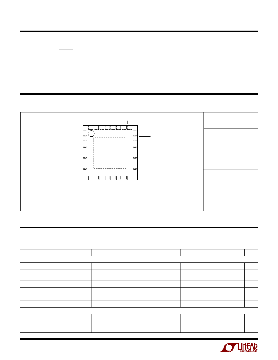
32 31 30 29 28 27 26 25
9
10 11 12 13 14 15 16
17
18
19
20
21
22
23
24
8
7
6
5
4
3
2
1
DV
CC
PRES A
C8A
C4A
I/O A
RST A
CLK A
V
CCA
FAULT
UNDERV
NC/NO
PRES B
I/O B
RST B
CLK B
V
CCB
SYNC
ASYNC
R
IN
DATA
D
OUT
D
IN
SCLK
LD
SGND
PGND
C
≠
SV
BATT
PV
BATT
C
+
CPO
NC
UH PACKAGE
32-LEAD PLASTIC QFN
PIN 1
TOP VIEW
UH PART MARKING
1955
LTC1955
3
sn1955 1955fs
ELECTRICAL CHARACTERISTICS
The
q
denotes the specifications which apply over the full operating
temperature range, otherwise specifications are at T
A
= 25
∞
C. V
PVBATT
= V
SVBATT
= 3.3V, DV
CC
= 3.3V unless otherwise noted.
SYMBOL
CONDITIONS
MIN
TYP
MAX
UNITS
Smart Card Supplies V
CCA
, V
CCB
V
CCA/B
Output Voltage
5V Mode, 0 < I
CCA/B
< 60mA
q
4.65
5.0
5.35
V
3V Mode, 0 < I
CCA/B
< 50mA
q
2.75
3.0
3.25
V
1.8V Mode, 0 < I
CCA/B
< 30mA
q
1.65
1.8
1.95
V
V
CCA/B
Turn On-Time
I
CCA/B
= 0mA, 10% to 90%
q
0.8
1.5
ms
Undervoltage Detection
Relative to Nominal Output
q
≠ 9
≠ 5
≠ 2.5
%
Overcurrent Detection
5V Mode
q
65
100
135
mA
Smart Card Detection
Debounce Time (
PRES A/B to
D15/D7) V
NC/NO
= 0V
q
20
35
60
ms
PRES A, PRES B Pull-Up Current
V
PRESA/B
= 0
q
1.25
2.5
µ
A
Deactivation Time (
RST to V
CC
= 0.4V)
I
CCA/B
= 0mA, C
VCCA/B
= 1
µ
F
q
20
250
µ
s
CLK A, CLK B
Low Level Output Voltage (V
OL
), (Note 2)
Sink Current = ≠ 200
µ
A
q
0.2
V
High Level Output Voltage (V
OH
), (Note 2)
Source Current = 200
µ
A
q
V
CCA/B
≠ 0.2
V
Rise/Fall Time, (Note 2)
Loaded with 50pF, 10% to 90%
q
16
ns
CLK A, CLK B Frequency, (Note 2)
q
10
MHz
RST A, RST B, C4A, C8A
Low Level Output Voltage (V
OL
), (Note 2)
Sink Current = ≠ 200
µ
A
q
0.2
V
High Level Output Voltage (V
OH
), (Note 2)
Source Current = 200
µ
A
q
V
CCA/B
≠ 0.2
V
Rise/Fall Time, (Note 2)
Loaded with 50pF, 10% to 90%
q
100
ns
I/O A, I/O B
Low Level Output Voltage (V
OL
), (Note 2)
Sink Current = ≠1mA (V
DATA
= 0V)
q
0.3
V
High Level Output Voltage (V
OH
), (Note 2)
Source Current = 20
µ
A (V
DATA
= V
DVCC
)
q
0.85 ∑ V
CCA/B
V
Rise/Fall Time, (Note 2)
Loaded with 50pF, 10% to 90%
q
500
ns
Short Circuit Current, (Note 2)
V
DATA
= 0V
q
5
10
mA
DATA
Low Level Output Voltage (V
OL
)
Sink Current = ≠ 500
µ
A (V
I/OA/B
= 0V)
q
0.3
V
High Level Output Voltage (V
OH
)
Source Current = 20
µ
A (V
I/OA/B
= V
CCA/B
)
q
0.8 ∑ DV
CC
V
Rise/Fall Time
Loaded with 50pF, 10% to 90%
q
500
ns
R
IN
, D
IN
, SCLK, LD, SYNC, ASYNC, NC/NO
Low Input Threshold (V
IL
)
q
0.15 ∑ DV
CC
V
High Input Threshold (V
IH
)
q
0.85 ∑ DV
CC
V
Input Current (I
IH
/I
IL
)
q
≠1
1
µ
A
D
OUT
Low Level Output Voltage (V
OL
)
Sink Current = ≠ 200
µ
A
q
0.3
V
High Level Output Voltage (V
OH
)
Source Current = 200
µ
A
q
DV
CC
≠ 0.3
V
UNDERV
Threshold
q
1.17
1.23
1.29
V
Leakage Current
V
UNDERV
= 3.3V
q
50
nA
LTC1955
4
sn1955 1955fs
ELECTRICAL CHARACTERISTICS
The
q
denotes the specifications which apply over the full operating
temperature range, otherwise specifications are at T
A
= 25
∞
C. V
PVBATT
= V
SVBATT
= 3.3V, DV
CC
= 3.3V unless otherwise noted.
PARAMETER
CONDITIONS
MIN
TYP
MAX
UNITS
Note 1: Absolute Maximum Ratings are those values beyond which the life
of a device may be impaired.
Note 2: This specification applies to all three smart card voltage classes:
1.8V, 3V and 5V.
Note 3: R
OLCP
(2V
BATT
≠ V
CPO
)/I
CPO
; V
CPO
will depend upon total load
(I
CCA
+ I
CCB
) and minimum supply voltage V
BATT
. See Figure 6.
FAULT
Low Level Output Voltage (V
OL
)
Sink Current = ≠ 200
µ
A
q
0.005
0.3
V
Leakage Current
V
FAULT
= 5.5V
q
1
µ
A
SYMBOL PARAMETER
CONDITIONS
MIN
TYP
MAX
UNITS
Serial Port Timing
t
DS
D
IN
Valid to SCLK Setup
q
8
ns
t
DH
D
IN
Valid to SCLK Hold
q
8
ns
t
DD
D
OUT
Output Delay
C
LOAD
= 15pF
q
15
60
ns
t
L
SCLK Low Time
q
50
ns
t
H
SCLK High Time
q
50
ns
t
LW
LD Pulse Width
q
50
ns
t
CL
SCLK to LD
q
50
ns
t
LC
LD to SCLK
q
0
ns
Note 4: The LTC1955E is guaranteed to meet performance specifications
from 0
∞
C to 70
∞
C. Specifications over the ≠ 40
∞
C to 85
∞
C operating
ambient temperature range are assured by design, characterization and
correlation with statistical process controls.
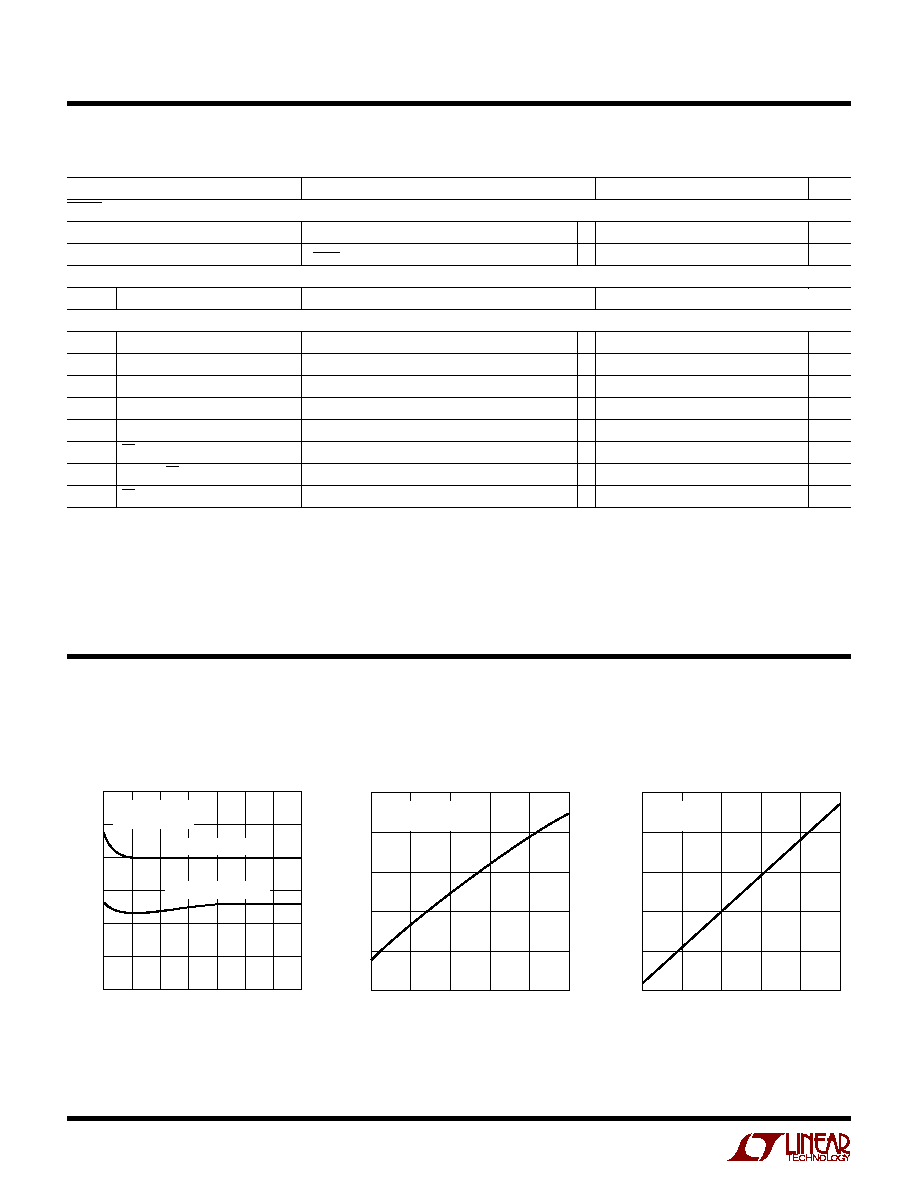
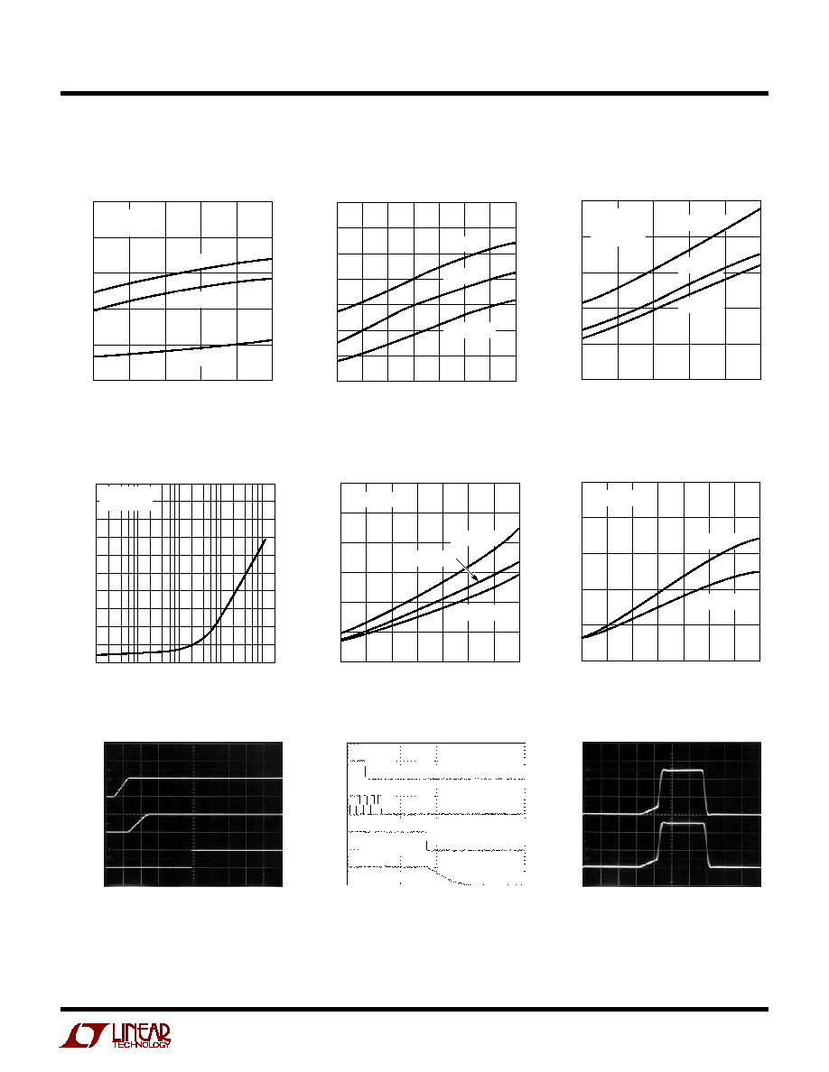
TYPICAL PERFOR A CE CHARACTERISTICS
U
W
SUPPLY VOLTAGE (V)
2.7
3.1
3.5
3.9
4.3
4.7
5.1
5.5
SUPPLY CURRENT (
µ
A)
1955 G01
600
500
400
300
200
100
0
T
A
= 25
∞
C
I
CCA
= I
CCB
= 0
µ
A
V
CCA
= V
CCB
= 5V
V
CCA
= 1.8V, V
CCB
= 0V
TEMPERATURE (
∞
C)
≠40
≠15
10
35
60
85
SHORT-CIRCUIT CURRENT (mA)
1955 G02
6.0
5.5
5.0
4.5
4.0
3.5
DV
CC
= V
BATT
= 5.5V
V
CCX
= 5V
TEMPERATURE (
∞
C)
≠40
≠15
10
35
60
85
OUTPUT RESISTANCE (
)
1955 G03
7.0
6.5
6.0
5.5
5.0
4.5
V
IN
= 2.7V
V
CPO
= 4.9V
No Load Supply Current vs V
BATT
I/O X Short-Circuit Current vs
Temperature
Charge Pump Open-Loop Output
Resistance vs Temperature
(2V
IN
≠ V
CPO
) / I
LOAD(MAX)
LTC1955
5
sn1955 1955fs
TYPICAL PERFOR A CE CHARACTERISTICS
U
W
TEMPERATURE (
∞
C)
≠40
≠15
10
35
60
85
LOAD CURRENT (mA)
1955 G04
180
160
140
120
100
80
V
BATT
= 3.3V
V
CPO
= 5.75V
V
CCX
= 1.8V
V
CCX
= 3V
V
CCX
= 5V
V
BATT
SUPPLY VOLTAGE (V)
2.7
3.1
3.5
3.9
4.3
4.7
5.1
5.5
DEBOUNCE TIME (ms)
1955 G05
60
55
50
45
40
35
30
25
T
A
= 85
∞
C
T
A
= 25
∞
C
T
A
= ≠40
∞
C
TEMPERATURE (
∞
C)
≠40
≠15
10
35
60
85
I/O A, I/O B LOW OUTPUT VOLTAGE (V)
1955 G06
0.16
0.14
0.12
0.10
0.08
0.06
V
DATA
= 0V
I
OL
= ≠1mA
V
BATT
= 2.7V
V
CCX
= 1.8V
V
CCX
= 3V
V
CCX
= 5V
LOAD CURRENT (A)
V
BATT
QUIESCENT CURRENT (mA)
10
9
8
7
6
5
4
3
2
1
0
10
µ
1m
10m
1955 G07
100
µ
100m
V
BATT
= 3.1V
T
A
= 25
∞
C
V
CCX
Overcurrent Shutdown
Threshold vs Temperature
Card Detection Debounce Time vs
V
BATT
Supply Voltage
Bidirectional Channel (I/O A, I/O B)
Low Output Level vs Temperature
V
BATT
Quiescent Current
[I
BATT
≠ 2 (I
CCA
+ I
CCB
)]
vs Load Current
V
BATT
Shutdown Current vs
Supply Voltage
DV
CC
Shutdown Current vs Supply
Voltage
Charge Pump and LDO Activation
Deactivation Sequence
Data ≠ I/O Channel, C
L
= 50pF
V
CPO
5V/DIV
V
CCA
5V/DIV
I/O A
5V/DIV
1ms/DIV
1955 G10
10
µ
s/DIV
1955 G11.eps
I/O A
2V/DIV
DATA
2V/DIV
100ns/DIV
1955 G12
RST A
5V/DIV
I/O A
5V/DIV
V
CCA
5V/DIV
CLK A
5V/DIV
V
BATT
SUPPLY VOLTAGE (V)
2.7
3.1
3.5
3.9
4.3
4.7
5.1
5.5
SUPPLY CURRENT (
µ
A)
1955 G08
3.0
2.5
2.0
1.5
1.0
0.5
0
T
A
= 85
∞
C
T
A
= 25
∞
C
T
A
= ≠40
∞
C
V
DVCC
= V
BATT
V
DVCC
SUPPLY VOLTAGE (V)
2.7
3.1
3.5
3.9
4.3
4.7
5.1
5.5
SUPPLY CURRENT (
µ
A)
1955 G09
1.0
0.8
0.6
0.4
0.2
0
T
A
= 25
∞
C, 85
∞
C
T
A
= ≠40
∞
C
V
DVCC
= V
BATT

LTC1955
6
sn1955 1955fs
ASYNC: Input. The ASYNC pin provides the clock input for
asynchronous cards and should be connected to a free
running clock. The clock signal to the smart card can be a
˜
1,
˜
2,
˜
4 or
˜
8 version of the signal on ASYNC. Asynchro-
nous cards can also be placed in clock stop mode with the
clock stopped either high or low.
D
IN
: Input. Input for the serial port. Command data is
shifted into D
IN
synchronously with SCLK. D
IN
can be
connected directly to a microcontroller or the D
OUT
pin of
another LTC1955 for daisy chained operation.
D
OUT
: Output. Output for the serial port. Smart card status
data is shifted out of D
OUT
synchronously with SCLK. D
OUT
can be connected directly to a microcontroller or the D
IN
pin of another LTC1955 for daisy chained operation.
SCLK: Input. The SCLK pin clocks the serial port. Each new
data bit is received on the rising edge of SCLK. SCLK
should be left high during idle times and should not be
clocked when LD is low.
LD: Input. The falling edge of this pin loads the current
state of the shift register into the command register.
Command changes to both smart card channels will be
updated on the falling edge of LD. The rising edge of LD
latches status information from the smart card channels
into the shift register for the next read/write cycle.
NC/NO: Input. This pin controls the activation level of the
PRES A/PRES B pins. When it is high (DV
CC
), the PRES
pins are active high. When it is low (GND), the PRES pins
are active low. When a ground side N.O. switch is used, the
NC/NO pin should be grounded. When a ground side N.C.
switch is used, the NC/NO pin should be connected to
DV
CC
.
Note: If an N.C. switch is used, a small current (several
microamperes) will flow through the switch whenever a
smart card is not present. For ultralow power consump-
tion in shutdown, an N.O. switch is optimum.
PI FU CTIO S
U
U
U
SV
BATT
: Power. Supply voltage for analog sections of the
LTC1955.
PV
BATT
: Power. Supply voltage for the charge pump.
DV
CC
: Power. Reference voltage for the control logic.
SGND: Ground. Signal ground for analog sections of the
LTC1955.
PGND: Ground. Power ground for the charge pump. This
pin should be connected directly to a low impedance
ground plane.
CPO: Charge Pump. CPO is the output of the charge pump.
When one or both of the smart cards requires power, the
charge pump will charge CPO to either 3.7V or 5.35V
depending on what smart card voltages are required. A low
impedance 4.7
µ
F X5R or X7R ceramic capacitor is re-
quired on CPO.
C
+
, C
≠
: Charge Pump. Charge pump flying capacitor pins.
A 1
µ
F X5R or X7R ceramic capacitor should be connected
from C
+
to C
≠
.
DATA: Input/Output. Microcontroller side data I/O pin. The
DATA pin provides the bidirectional communication path
to both smart cards. One, both or neither of the cards may
be selected to communicate via the DATA pin. If several
LTC1955s are connected in parallel, the DATA pin can be
made high impedance by selecting neither card. The C4A
and C8A synchronous card pins can be selected to con-
nect to the DATA pin via the serial port (see Table 4).
R
IN
: Input. The R
IN
pin supplies the RST signal to both
smart cards. It is level shifted and transmitted directly to
the RST pin of a selected card socket. When a card is
deselected, the RST A/RST B pin for that channel is latched
at its current state.
SYNC: Input. The SYNC pin provides the clock input for
synchronous smart cards. When a synchronous card is
selected, its CLK pin follows SYNC directly. When a
synchronous card is deselected, the CLK A/CLK B pin for
that channel is latched at its current state.

LTC1955
7
sn1955 1955fs
PRES A/PRES B: Card Socket. The PRES A/PRES B pins
are used to detect the presence of the smart cards. They
can be connected to either normally open or normally
closed detection switches on the smart card acceptor's
sockets. The NC/NO pin should be set appropriately. These
pins have a pull-up current source on-chip so no external
components are required.
C4A/C8A: Card Socket. These pins connect to the C4 and
C8 pins of synchronous memory cards on smart card
socket A. The signal for these pins is unidirectional and can
only be sent to the card. Data for C4A and C8A is transmit-
ted via the DATA pin and may be selected in place of I/OA
via the serial port (see Table 4). When either C4A or C8A
is selected, it will follow the DATA pin. When it is dese-
lected, it will remain latched at its current state.
I/O A/I/O B: Card Socket. The I/O A/I/O B pins connect to
the I/O pins of the respective smart card sockets. When a
smart card is selected, its I/O pin connects to the DATA pin.
When a smart card is deselected, its I/O A/I/O B pin returns
to the idle state (H).
RST A/RST B: Card Socket. These pins should be con-
nected to the RST pins of the respective smart card
sockets. The RST A/RST B signals are derived from the R
IN
pin. When a card is selected, its RST pin follows R
IN
. When
a card is deselected, the RST A/RST B pin for that channel
holds the current value on R
IN
.
CLK A/CLK B: Card Socket. The CLK A/CLK B pins should
be connected to the CLK pins of the respective smart card
sockets. The CLK A/CLK B signals can be derived from
either the SYNC input or the ASYNC input depending on
which type of card is being accessed. The card type is
selected via the serial port (see Tables 1 and 3).
V
CCA
, V
CCB
: Card Socket. The V
CCA
/V
CCB
pins should be
connected to the V
CC
pins of the respective smart card
sockets. The activation of a V
CCA
/V
CCB
pin is controlled by
the serial port (see Tables 1 and 2) and can be set to 0V,
1.8V, 3V or 5V. The voltage levels of the two card sockets
are controlled independently for maximum flexibility.
FAULT: Output. The FAULT pin can be used as an interrupt
to a microcontroller to indicate when a fault has occurred.
It is an open drain output, which is logically equivalent to
D4 + D5 + D12 + D13. (See Table 1)
UNDERV: Input. The UNDERV pin provides security by
supplying a precision undervoltage threshold for external
supply monitoring. An external resistive voltage divider
programs the desired undervoltage threshold. Once
UNDERV falls below 1.23V, the LTC1955 automatically
begins the deactivation sequence on any channel that is
active.
If external supply monitoring is not required, the UNDERV
pin should be connected to either SV
BATT
or DV
CC
.
PI FU CTIO S
U
U
U
LTC1955
8
sn1955 1955fs
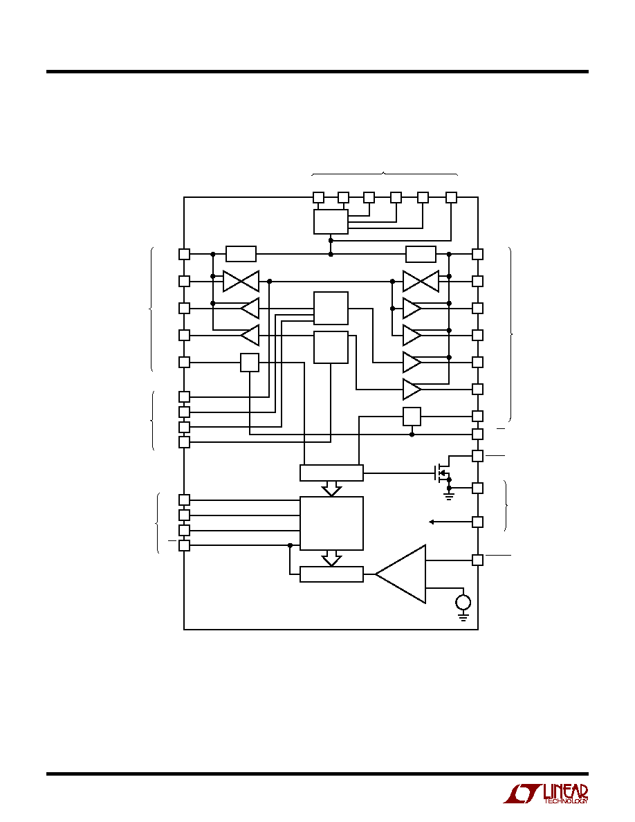
BLOCK DIAGRA
W
C4A
C8A
I/O A
RST A
V
CCB
CLK A
V
CCA
SV
BATT
DV
CC
PGND
CHARGE PUMP
FAULT
NC/NO
UNDERV
1.23V
SGND
PRES A
1955 BD
SMART
CARD
SOCKET B
SMART
CARD
SOCKET A
DIGITAL
SUPPLY
SMART
CARD
COMMUNICATIONS
SERIAL PORT
COMMAND/STATUS
DATA
C
+
C
≠
CPO
+
≠
RESET
CONTROL
LOGIC
STATUS DATA
COMMAND LATCH
SHIFT REGISTER
+
≠
LDO A
CLK B
RST B
I/O B
PRES B
D
IN
D
OUT
SCLK
LD
LDO B
CLOCK
CONTROL
LOGIC
CHARGE
PUMP
DATA
ASYNC
SYNC
R
IN
25
26
28
27
30
32
31
29
21
19
18
20
17
24
9
1
23
22
2
6
7
3
4
5
8
14
11
10
12
PV
BATT
13
15
LTC1955
9
sn1955 1955fs
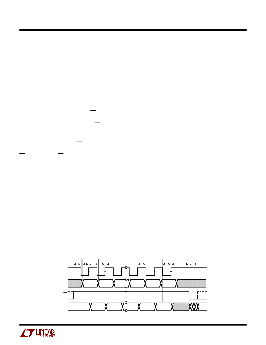
Serial Port
The microcontroller compatible serial port provides all of
the command and control inputs for the LTC1955 as well
as the status of the two smart cards. Data on the D
IN
input
is loaded on the rising edge of SCLK. D15 is loaded first
and D0 last. At the same time the command bits are being
shifted into the D
IN
input, the status bits are being shifted
out of the D
OUT
output. The status bits are presented to
D
OUT
on the rising edge of SCLK. Once all bits have been
clocked into the shift register, the command data is loaded
into the command latch by bringing LD low. At this time
the command latch is updated and the LTC1955 will begin
to act on the new command set. When LD is low, the shift
register is transparent to the status data of the two smart
card channels. The status data is latched into the shift
register on the rising edge of LD. SCLK should be held in
the high state when idle and should only be clocked when
LD is high. Likewise LD should only be brought high when
SCLK is high. Figure 2 shows the operation of the serial
port.
Multiple LTC1955s may be daisy-chained together by
connecting the D
OUT
pin of one LTC1955 to the D
IN
pin of
another. Figure 7 shows an example of multiple LTC1955s
daisy chained together.
The maximum clock rate for the serial port is 10MHz.
The serial port controls the following parameters of each
smart card socket:
∑ Selection/deselection of a smart card
∑ V
CC
voltage level of each card (5V/3V/1.8V/0V)
∑ Clock mode of each card (synchronous or asynchro-
nous)
∑ Operating mode of asynchronous cards (clock stop
high, low,
˜
1,
˜
2,
˜
4 or
˜
8)
∑ Selection of the I/O, C4 or C8 pins for card socket A
The serial port provides the following status data:
∑ It indicates the presence or absence of the smart cards.
∑ It indicates the readiness of the smart card V
CC
sup-
plies. Communication with a smart card is disabled
until its power supply voltage has reached the final
value.
∑ It indicates fault status. In the event of an electrical or
ATR fault, the fault is reported. For electrical faults, the
LTC1955 will automatically deactivate the smart card.
Table 1 illustrates the command inputs and status outputs
associated with each bit of the serial data word.
Three voltage options are available from the LTC1955: 5V,
3V and 1.8V. Bits D0, D1 (card B) and D8, D9 (card A)
determine which voltage is selected. Setting both control
bits of a channel to 0 deactivates that channel and sets the
smart card supply voltage to 0V. If both channels are
deactivated, the LTC1955 is in shutdown. Table 2 shows
the operation of the supply control bits.
The CLK A/CLK B pins to the smart cards can be pro-
grammed for various modes. Both synchronous and asyn-
chronous cards are supported. There are several options
available with asynchronous cards. Table 3 shows how all
clock options are obtained using bits D5≠D7 (card B) and
D13≠D15 (card A). The default state of the LTC1955 on
power up is synchronous mode.
Figure 2. Serial Port Timing Diagram
D
IN
SCLK
LD
X
D0
D15
X
D1
D
OUT
D15 FROM
INPUT
D0
D15
1955 F02
D14
D13
D15
D1
t
LC
t
DH
t
DD
t
DS
t
H
t
L
t
LW
t
CL
D14
D2
OPERATIO
U
LTC1955
10
sn1955 1955fs
To receive status data from the serial port, a read/write
operation must be performed. When polling for the pres-
ence of a smart card on both channels, the input word
should be set to $0000 since this is the shutdown com-
mand for the LTC1955. However, consider the example
where some operation is already being performed on
channel A. If, for example, the previous command was
$BE00 (V
CCA
set to 3V, card selected, I/O A connected to
DATA and CLK A set to ASYNC
˜
2), then the commands for
this channel must be rewritten to the serial port each time.
To poll for the presence of a card on channel B, or even the
V
CCA
READY status, then $BE00 should be rewritten on
each new read/write cycle. Once a card is detected on
channel B, the commands for channel B can be changed
but the $BExx should continue to be rewritten for channel
A.
Bidirectional Channels
The bidirectional channels are level shifted to the appropri-
ate V
CCA/B
voltages at the I/O A/I/O B pins.
An NMOS pass transistor performs the level shifting. The
gate of the NMOS transistor is biased such that the
transistor is completely off when both sides have relin-
quished the channel. If one side of the channel asserts an
L, then the transistor will convey the L to the other side.
Note that current passes from the receiving side of the
channel to the transmitting side. The low output voltage of
the receiving side will be dependent upon the voltage at the
transmitting side plus the I ∑ R drop of the pass transistor.
When a card socket is selected, it becomes a candidate to
drive data on the DATA pin and likewise receive data from
the DATA pin. When a card socket is deselected, the
voltage on its I/O A/I/O B pin will return to the idle state (H)
and the DATA side of that channel will become high
impedance. If both cards are deselected, the DATA pin will
be high impedance.
Both cards may be deselected at the same time to allow
communication with a second LTC1955.
Card channel A includes provision for unidirectional com-
munication with the C4 and C8 pins of the smart card. The
C4, C8 and I/O pins of card A are individually multiplexed
to the DATA pin using bits D11 and D12 as shown in
Table 4.
Table 1. Serial Port Commands
STATUS OUTPUT
BIT
COMMAND INPUT
CARD B
0
D0
V
CCB
Options
0
D1
(See Table 2)
0
D2
Card B Select/Deselect
0
D3
Data Pull-Up Defeat
Card B Electrical Fault
D4
Reserved (Always Set to "0")
Card B ATR Fault
D5
Card B Clock Options
Card B V
CC
Ready
D6
(See Table 3)
Card B Present
D7
CARD A
0
D8
V
CCA
Options
0
D9
(See Table 2)
0
D10 Card A Select/Deselect
0
D11 Card A Communications
Card A Electrical Fault
D12 Options (See Table 4)
Card A ATR Fault
D13 Card A Clock Options
Card A V
CC
Ready
D14 (See Table 3)
Card A Present
D15
Table 2. V
CC
and Shutdown Options
D9
D8
Status (Card A)
D1
D0
Status (Card B)
0
0
V
CC
= 0V (Shutdown)
0
1
V
CC
= 1.8V
1
0
V
CC
= 3V
1
1
V
CC
= 5V
Table 3. Clock Options
D7
D6
D5
Clock Mode Card B
D15
D14
D13
Clock Mode Card A
0
0
0
Synchronous Mode
0
0
1
Unused
0
1
0
Asynchronous Stop Low
0
1
1
Asynchronous Stop High
1
0
0
Asynchronous
˜
1
1
0
1
Asynchronous
˜
2
1
1
0
Asynchronous
˜
4
1
1
1
Asynchronous
˜
8
OPERATIO
U
LTC1955
11
sn1955 1955fs
Note that if a reset is initiated with both cards selected,
then both may give an answer to reset and collide on the
DATA line. No damage will occur but data could be lost or
corrupted.
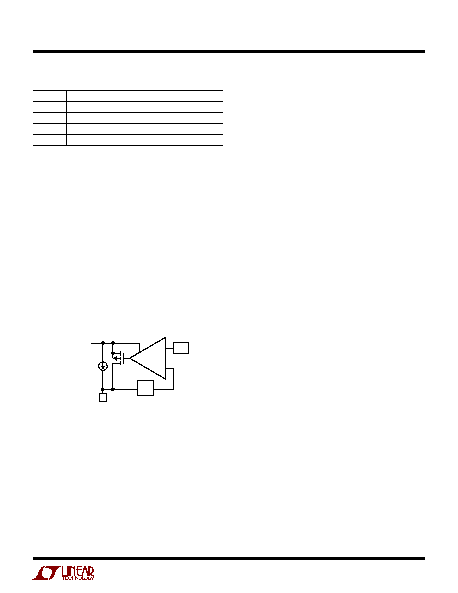
Dynamic Pull-Up Current Sources
The current sources on the bidirectional pins (DATA, I/O A/
I/O B) are dynamically activated to achieve a fast rise time
with a relatively small static current*. Once a bidirectional
pin is relinquished, a small start up current begins to
charge the node. An edge rate detector determines if the
pin is released by comparing its slew rate with an internal
reference value. If a valid transition is detected, a large
pull-up current enhances the edge rate on the node. The
higher slew rate corroborates the decision to charge the
node thereby affecting a dynamic form of hysteresis.
In asynchronous mode the CLK A/CLK B pins follow either
the ASYNC pin (
˜
1 mode) or a divided version of this pin.
The CLK A/CLK B pins can also be stopped high or low. The
available divider ratios include
˜
2,
˜
4 and
˜
8. When
switching between divider ratios, the internal selection
circuitry ensures that no spikes or glitches appear on the
CLK A/CLK B pins. Consequently, it may take up to 8 clock
pulses for the clock frequency change command to take
affect. Synchronization circuitry ensures that no glitches
occur when entering or exiting one of the stop modes. For
example, when entering stop low mode, the selection
circuitry waits for the next falling edge of the respective
CLK A/CLK B signal to make the change. Likewise if stop
high is selected it will occur on the next rising edge.
Deselection of an asynchronous card does not affect its
CLK A/CLK B pin. Its clock can be started, stopped or its
divider ratio changed at any time.
To clean up the duty cycle of the incoming clock in
asynchronous applications, any of the clock divider modes
˜
2,
˜
4 or
˜
8 will yield a very nearly 50% duty cycle.
Additional synchronization circuitry prevents glitches from
occurring when switching between synchronous mode
and asynchronous mode. Because of this circuitry, two
edges (a falling edge followed by a rising edge) are
necessary at the CLK pin to switch modes from asynchro-
nous to synchronous. For example, if clock stop mode is
engaged, the clock channel will not change modes until
clock stop mode is disengaged.
Any combination of cards, synchronous or asynchronous,
can be used as both channels can be set to any of the clock
modes or divider ratios independently.
Both SYNC and ASYNC inputs are independently level
shifted to the appropriate voltage for the CLK A/CLK B pins
(5V, 3V, 1.8V).
Reset Channels
When a card is selected, the reset channels provide a level
shifted path from the R
IN
pin to the RST A/RST B pins.
When a card is deselected its RST A/RST B pin is latched
at the current value of R
IN
.
Table 4. Card A Communications Options
D12
D11
Card A Communication Mode
0
0
Nothing Selected
0
1
C4A Connected to DATA Pin
1
0
C8A Connected to DATA Pin
1
1
I/O A Connected to DATA Pin
Figure 3. Dynamic Pull-Up Current Sources
≠
+
dv
dt
V
REF
LOCAL
SUPPLY
BIDIRECTIONAL
PIN
1955 F03
I
START
Clock Channels
As described in the section Serial Port, the LTC1955
supports both synchronous and asynchronous smart
cards. On start-up, or when bits D13-D15 for card A and
bits D5-D7 for card B are set to 0s, the clock channel is in
synchronous mode. The remaining modes are used for
asynchronous cards.
In synchronous mode the CLK A/CLK B pins follow the
SYNC pin for a channel that is selected. If a channel is
deselected (via the serial port) the CLK A/CLK B line for that
channel is latched at its current value.
OPERATIO
U
*U.S. Patent No. 6,356,140

LTC1955
12
sn1955 1955fs
Smart Card Detection Circuits
The PRES A/PRES B pins are used to detect the presence
of a smart card. An automatic debounce circuit waits until
a smart card has been present for a continuous period of
typically 35ms. Once a valid card indication exists, the
status bit for that channel is updated and may be polled by
cycling data through the serial port. The D
OUT
pin (equiva-
lent to D15) of the serial port can be used to indicate the
presence of a card on channel A in real time if LD is held
low.
The PRES A/PRES B pins have built-in pull-up current
sources so no external components are required for
switch detection. The pull-up current sources are de-
signed to have a small current when the pin voltage is
below approximately 1V but somewhat higher current
when the pin voltage reaches 1V. This helps maintain low
power dissipation when a card is present and yet fast
response time to a card removal.
The PRES A/PRES B pins can be configured to respond to
either normally open or normally closed switches via the
NC/NO pin.
Activation/Deactivation
For maximum flexibility, the activation sequencing of the
smart card is left to the application programmer. Upon
activation, to comply with relevant smart card standards,
none of the smart card signal pins will be allowed to go
high before the smart card supply voltage (V
CCA
/V
CCB
) has
reached its final value. Deactivation can be achieved either
manually or automatically. An electrical fault condition will
trigger the automatic deactivation.
Manual deactivation may be performed under software
control by setting the smart card pins to 0V in the desired
sequence via the control pins (SYNC, ASYNC, R
IN
, DATA
and the serial port). For most applications this will be
cumbersome and the built-in deactivation will be used
instead.
Automatic Deactivation
The built-in deactivation sequence can be executed via the
serial port simply by setting the appropriate control bits
(D0 and D1 or D8 and D9) to 0. The deactivation sequence
is outlined below.
1. The RST A/RST B pin for that channel is immediately
brought low.
2. The deactivation of the CLK A/CLK B pins depends upon
which type of card is used:
If the smart card was set to asynchronous mode then
the CLK A/CLK B pin will be latched low on its next falling
edge. If no falling edges occur within 5
µ
s (min) then the
CLK A/CLK B line is forced low.
If the smart card was set to synchronous mode then the
CLK A/CLK B pin is immediately latched at its current
value (either high or low) and then forced low after a
duration of 5
µ
s (min). During the 5
µ
s timeout period
changes on SYNC will be ignored.
3. The I/O A/I/O B, C4A and C8A pins for that channel are
brought low.
4. The V
CCA
/V
CCB
pin is brought low.
If an error occurs on one smart card, operation of the other
card is unaffected.
OPERATIO
U

LTC1955
13
sn1955 1955fs
Electrical Fault Detection
Several types of faults are detected by the LTC1955. They
include V
CCA
/V
CCB
undervoltage, V
CCA
/V
CCB
overcurrent,
CLK A/CLK B, RST A/RST B, C8A, C4A short circuit, card
removal during a transaction, failed answer to reset (ATR),
supply undervoltage or UNDERV and chip overtemperature.
To prevent false errors from plaguing the microcontroller,
the electrical faults are acted upon only after a 5
µ
s (min)
timeout period. Card removal during transaction faults
initiate the deactivation sequence immediately.
V
CCA
/V
CCB
under voltage faults are determined by com-
paring the actual output voltage with the internal reference
voltage. If the output is more than ~5% below its set point
for the entire timeout period, the fault is reported and the
deactivation sequence is initiated.
V
CCA
/V
CCB
overcurrent faults are detected by comparing
the output current of the LDOs with an internal reference
level. If the current of an LDO is more than 100mA (typ) for
the entire timeout period, the fault is reported and the
deactivation sequence is initiated.
CLK A/CLK B and RST A/RST B faults are detected by
comparing the outputs of these pins with their expected
signals. If the signal on a pin is incorrect for the entire
timeout period, the fault is reported and the deactivation
sequence is initiated.
The clock channels are a special case. Since they can have
a free running clock, the error indication is accumulated
over a longer period of time without being cleared. Even
though the clock may be running, an error will still be
detected.
An overtemperature fault is detected by sensing the junc-
tion temperature of the IC. If the junction temperature
exceeds approximately 150
∞
C for the entire timeout
period, the fault is reported by setting both fault bits (D4
and D12) and the deactivation sequence is initiated.
A card removal fault is determined as soon as the PRES A/
PRES B pin is high (for NC/NO = 0). Once this occurs the
fault is reported and the deactivation sequence is initiated.
If no card is present, and the application software attempts
to power up a card socket, an automatic fault will result on
that channel.
OPERATIO
U
Short circuits on the I/O A/I/O B lines will not be detected
by the fault detection hardware; however, a short circuit
from these lines to their respective V
CCA
/V
CCB
pins will be
compliant with the maximum current limits set by appli-
cable standards (<15mA).
Answer to Reset (ATR) Fault Detection
Answer to Reset faults are detected by an internal counter
that is started once the RST A/B line goes high. If the DATA
pin remains high for 40,000 clock cycles, the ATR fault bit
for a given channel is set in the serial port's status register
(see Table 1) and the FAULT pin is brought low.
An ATR fault can not occur if the clock mode of a channel
is set to synchronous. ATR faults will only occur for
asynchronous smart cards.
ATR faults are cleared by bringing the RST A/B pin low for
the faulted channel. This will also clear the FAULT pin to
the Hi-Z state (assuming no other errors are causing
FAULT to be low).
An ATR fault will not automatically deactivate a card
channel. It is the application programmer's responsibility
to check the status register for ATR faults and deactivate
the smart card channel in accordance with smart card
standards. Generally the application has 50ms (EMV
2.1.3.1, 2.1.3.2) from the 40,000th clock pulse to deacti-
vate the card. Once the LTC1955 receives the deactivation
command, it will shut down a card channel in less than
250
µ
s.
Using the FAULT Pin
The FAULT pin can be used as an interrupt to a
microcontroller. It is an open-drain output and generally
requires a pull-up resistor. The FAULT pin will go low when
either an electrical fault or an answer to reset fault occurs
on either channel. Thus there are four possible faults that
can cause it to indicate a problem. The serial port's status
register must be polled to find out what type of fault
occured and on which channel. The FAULT pin is logically
equivalent to D4+D5+D12+D13 (see Table 1).
LTC1955
14
sn1955 1955fs
10kV ESD Protection
All smart card pins (CLK A/CLK B, RST A/RST B, I/O A/
I/O B, C4A, C8A and V
CCA
/V
CCB
) can withstand over 10kV
of human body model ESD in-situ. In order to ensure
proper ESD protection, careful board layout is required.
The PGND and SGND pins should be tied directly to a
ground plane. The V
CCA
/V
CCB
capacitors should be located
very close to the V
CCA
/V
CCB
pins and tied immediately to
the ground plane.
Capacitor Selection
Warning: A polarized capacitor such as tantalum or alumi-
num should never be used for the flying capacitor since its
voltage can reverse upon start up of the LTC1955. Low
ESR ceramic capacitors should always be used for the
flying capacitor.
A total of six capacitors are required to operate the
LTC1955. An input bypass capacitor is required at PV
BATT
,
SV
BATT
and DV
CC
. Output bypass capacitors are required
on each of the smart card V
CCA
/V
CCB
pins. A charge pump
flying capacitor is required from C
+
to C
≠
and a charge
storage capacitor is required on the charge pump out pin
CPO.
To prevent excessive noise spikes due to charge pump
operation, low ESR (equivalent series resistance) multi-
layer ceramic capacitors are strongly recommended.
There are several types of ceramic capacitors available
each having considerably different characteristics. For
example, X7R/X5R ceramic capacitors have excellent volt-
age and temperature stability but relatively low packing
density. Y5V ceramic capacitors have apparently higher
packing density but poor performance over their rated
voltage or temperature ranges. Under certain voltage and
temperature conditions, Y5V and X7R/X5R ceramic ca-
pacitors can be compared directly by case size rather than
specified value for a desired minimum capacitance.
Placement of the capacitors is critical for correct operation
of the LTC1955. Because the charge pump generates large
current steps, all of the capacitors should be placed as
close to the LTC1955 as possible. The low impedance
nature of multilayer ceramic chip capacitors will minimize
voltage spikes but only if the power path is kept very short
APPLICATIO S I FOR ATIO
W
U
U
U
(i.e., minimum inductance). The PV
BATT
/SV
BATT
nodes
should be especially well bypassed. The capacitor for this
node should be directly adjacent to the QFN package. The
C
PO
and flying capacitors should be very close as well. The
LTC1955 can tolerate more distance between the LDO
capacitors and the V
CCA/B
pins.
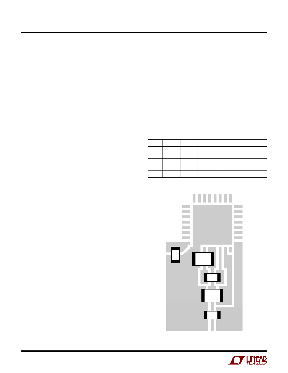
Figure 4 shows an example of a tight printed circuit board
using single layer copper. For best performance a multi-
layer board can be used and should employ a solid ground
plane on at least one layer.
The following capacitors are recommended for use with
the LTC1955:
Type
Value
Case Size
Murata P/N
C
IN
X5R
4.7
µ
F
0805
GRM40-034 X5R 475K 6.3
CPO
C
FLY
X5R
1
µ
F
0603
GRM39 X5R 105K 6.3
V
CCA/B
CDV
CC
X5R
0.1
µ
F
0402
GRM36 X5R 104K 10
V
CCA
GND
V
BATT
V
CCB
1955 F04
Figure 4. Optimum Single Layer PCB Layout
LTC1955
15
sn1955 1955fs
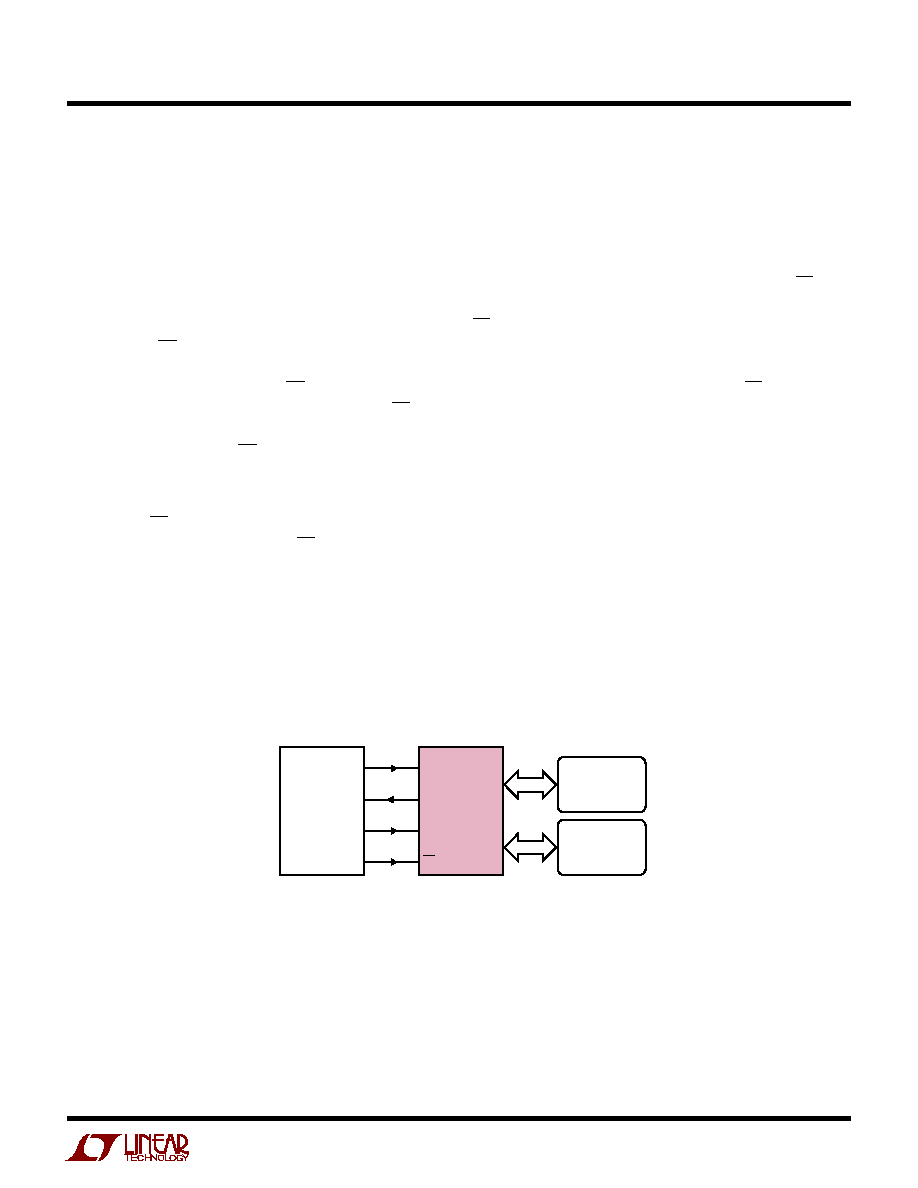
Interfacing to a Microcontroller
The serial port of the LTC1955 can be connected directly
to a 68HC11 style microcontroller's serial port. The
microcontroller should be configured as the master device
and its clock's idle state should be set to high (MSTR = 1,
CPOL = 1 and CPHA = 0 for the MC68HC11 family).
Figure 4 shows the recommended configuration and di-
rection of data flow. Note that an additional I/O line is
necessary for LD to load the data once it has shifted around
the loop. Command data is latched into the command
register on the falling edge of the LD signal. The LTC1955
will begin to act on new command data as soon as LD goes
low. Any general purpose microcontroller I/O line can be
configured to control the LD pin.
The status of the LTC1955 is returned over the serial port.
Status data is latched into the shift register on the rising
edge of the LD pin. Whenever the system is waiting for
status data from the LTC1955, its LD pin should be held
low.
Figure 5. Microcontroller Interface
CARD A
CARD B
1955 F05
D
IN
D
OUT
SCLK
LD
LTC1955
MOSI
MISO
SCK
I/O
µ
CONTROLLER
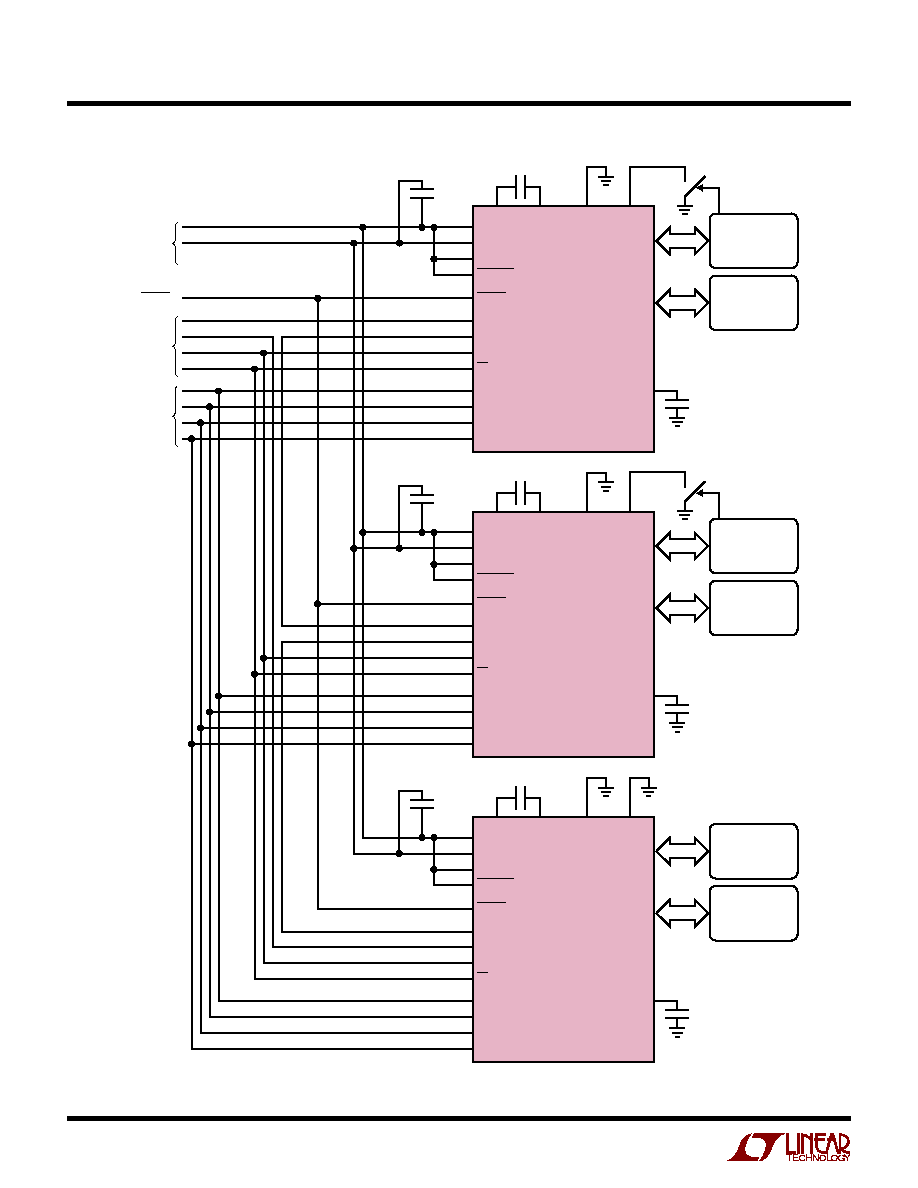
Daisy-Chained Operation
For applications requiring more than two card sockets, the
serial port of the LTC1955 is designed to be easily daisy-
chained. The D
OUT
pin of one LTC1955 can be connected
directly to the D
IN
pin of another LTC1955. Rather than
sending two 8-bit bytes before asserting LD, the
microcontroller should send two 8-bit bytes per device.
LD should only be asserted after all devices have been
updated. Figure 7 shows three LTC1955s cascaded in
daisy chain fashion. In this case the microcontroller would
write six 8-bit bytes before asserting the LD pin. Alterna-
tively, if two serial ports are available on the microcontroller,
then two LTC1955s can be controlled independently.
If the DATA lines of two or more LTC1955s are connected
together, the static pull-up current will be the sum of the
devices. The static current can be brought back to the level
of a single LTC1955 by setting bit D3 on all but one of the
LTC1955s to 1 (see Table 1). Bit D3 disables the pull-up
current source on the DATA pin. This will help prevent V
OL
problems in multiple LTC1955 applications when driving
the DATA or I/O pins low.
APPLICATIO S I FOR ATIO
W
U
U
U

LTC1955
16
sn1955 1955fs
Using S.A.M. Cards
For applications using one or more installed S.A.M. cards,
the PRES A/PRES B pins for those sockets must be
grounded before operation of the card can occur (assum-
ing NC/NO is grounded). The PRES A/PRES B pull-up
current is designed for very low consumption, but ultralow
current can be achieved in shutdown by using a
microcontroller output to pull down on the PRES A/PRES
B pins only when communication is necessary. The fault
detection circuitry will not allow a card socket to be
operated unless a card is detected.
Asynchronous Channel A Card Detection
Since the shift register is transparent when LD is held low,
D
OUT
is the same as D15. Recall from Table 1 that D15
indicates the status of the card detection channel for
channel A. Thus, it is not necessary to perform an entire
read/write operation to determine the card detection sta-
tus of channel A. With LD low, D
OUT
can be used to
generate a real time card detection interrupt. This could be
useful for one S.A.M. card, one smart card applications.
Inter Card Communication
Communication is possible directly from one card socket
to the other when both cards are selected at the same time.
This can be achieved by the following sequence of actions.
1) Start with both cards off and deselected
2) Activate the supply of the slave card
3) Select the slave card only
4) Initiate a reset on the slave card
5) Deselect the slave card
6) Activate the supply of the master card
7) Select the master card only
8) Initiate a reset on the master card
9) Select both cards
Using the UNDERV Pin
The UNDERV pin can be used to add protection against a
supply undervoltage fault. By using two external program-
ming resistors, the undervoltage detection can be set to an
arbitrary level (Figure 8). To ensure that the smart cards
are properly shut down, there must be sufficient energy
available in the input bypass capacitor to run one or both
smart cards until the deactivation cycle begins. It can take
approximately 30
µ
s from the detection of a fault until the
deactivation sequence begins. It is desirable to maintain
the V
BATT
supply at 2.7V or greater during this period.
Consider the following (worst-case) example:
1) The UNDERV pin is programmed to trip below 3.1V.
2) It is possible to have both cards activated at 5V and
drawing 60mA.
Since the output voltage is programmed to 5V, the charge
pump will be acting as a voltage doubler. With two cards
drawing 60mA each, the input current will be 2 ∑ (60mA +
60mA) or about 240mA. Allowing the V
BATT
supply to
droop from 3.1V to 2.7V during the 30
µ
s timeout period,
the input capacitance would need to be at least
240mA / [(3.1V ≠ 2.7V) / 30
µ
s] or 18
µ
F.
Thermal Management
To minimize power dissipation, the LTC1955 will actively
decide whether to step up or down depending on the
required output voltages and available input voltage. How-
ever, for optimum efficiency, the LTC1955 should be
powered from a 3.3V supply.
If the input voltage is above 3.6V, and both cards are
drawing maximum current, there can be substantial power
dissipation in the LTC1955. If the junction temperature
increases above approximately 150
∞
C, the thermal shut-
down circuitry will automatically deactivate both chan-
nels. To reduce the maximum junction temperature, a
good thermal connection to the PC board is recom-
mended.
Zero Shutdown Current
Although the LTC1955 is designed to have very low
shutdown current, it can still draw over a microampere on
APPLICATIO S I FOR ATIO
W
U
U
U
LTC1955
17
sn1955 1955fs
both DV
CC
and V
BATT
when in shutdown. For applications
that require virtually zero shutdown current, the DV
CC
pin
can be grounded. This will reduce the V
BATT
current to well
under a single microampere. Internal logic ensures that
the LTC1955 is in shutdown when DV
CC
is grounded.
Note, however, that all of the logic signals that are refer-
enced to DV
CC
(D
IN
, SCLK, LD, DATA, R
IN
, SYNC, ASYNC
and NC/NO) will have to be at 0V as well to prevent ESD
diodes to DV
CC
from being forward biased.
Operation at Higher Supplies
If a 5.5V to 6V supply voltage is available, it is possible to
achieve some power savings by bypassing the charge
pump. The higher supply can be connected directly to the
CPO pin. As long as the voltage on CPO is higher than that
at which it ordinarily regulates (5.35V or 3.7V depending
on voltage selections) the charge pump's oscillator will
not run. This configuration can give considerable power
savings since the charge pump is not being used.
A voltage source is still needed on both DV
CC
and SV
BATT
/
PV
BATT
in this configuration. Recall that DV
CC
sets the
logic reference level for all the control and smart card
communication pins. The voltage on SV
BATT
/PV
BATT
can
be any convenient level that meets the parameters in the
Electrical Characteristics table.
The 5.5V to 6V supply can be left permanently connected
to CPO but there will be approximately 5
µ
A of current flow
into CPO when the LTC1955 is in shutdown.
Charge Pump Strength
Under low V
BATT
conditions, the amount of current avail-
able to the smart cards is limited by the charge pump.
Figure 6 shows how the LTC1955 can be modeled as a
Thevenin equivalent circuit to determine the amount of
current available given the effective input voltage, 2V
BATT
and the effective open-loop output resistance, R
OLCP
.
From Figure 6, the available current is given by:
I
I
V
V
R
CCA
CCB
BATT
CPO
OLCP
+
2
≠
APPLICATIO S I FOR ATIO
W
U
U
U
R
OLCP
is dependent on a number of factors including the
switching term, 1/(f
OSC
∑ C
FLY
), internal switch resis-
tances and the nonoverlap period of the switching circuit.
However, for a given R
OLCP
, the minimum CPO voltage can
be determined from the following expression:
V
V
I
I
R
CPO
BATT
CCA
CCB
OLCP
+
2
≠ (
)
The LDOs have been designed to meet all applicable smart
card standards for V
CC
with V
CPO
as low as 5.13V. Given
this information, trade-offs can be made by the user with
regard to total consumption (I
CCA
+ I
CCB
) and minimum
supply voltage.
+
≠
LDO A
2V
BATT
1955 F06
CPO
R
OLCP
V
CCA
LDO B
V
CCB
Changing the Smart Card Supply Voltage
Although the LTC1955 control system will allow the smart
card voltage to be changed from one value to the next
without an interim power down, this is not recommended.
When changing from a higher voltage to a lower voltage
there will generally not be a problem; however, changing
from a lower voltage to a higher voltage will result in both
an undervoltage condition and an overcurrent condition
on that channel. The likely result is that the channel will
automatically deactivate. Applicable smart card standards
specify that the smart card supply be powered to zero
before applying a new voltage.
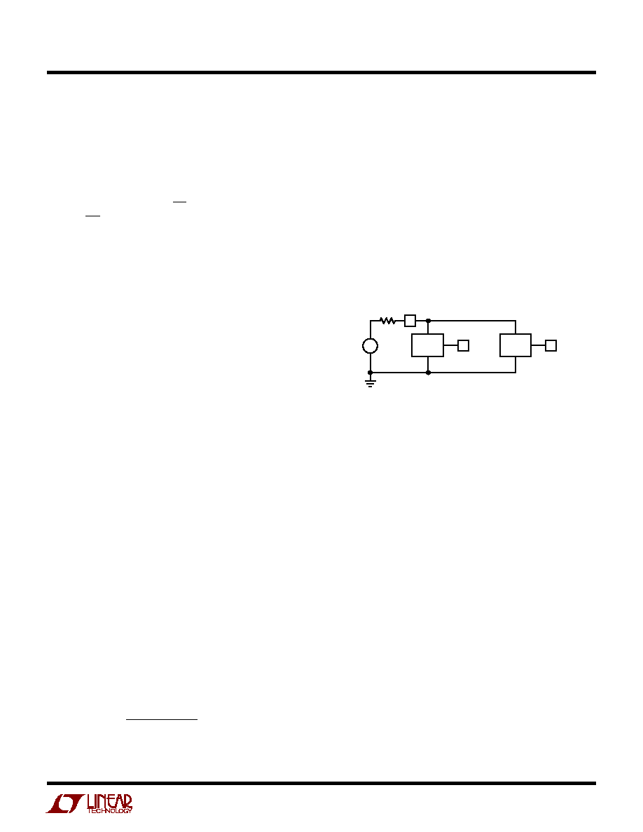
Compliance Testing
Inductance due to long leads on type approval equipment
can cause ringing and overshoot that leads to testing
problems. Small amounts of capacitance and damping
resistors can be included in the application without com-
promising the normal electrical performance of the
LTC1955 or smart card system. Generally a 100
resistor
and a 20pF capacitor will accomplish this as shown in
Figure 9.
Figure 6. Equivalent Open-Loop Circuit
LTC1955
18
sn1955 1955fs
APPLICATIO S I FOR ATIO
W
U
U
U
Figure 7. Multiple LTC1955s Daisy Chained Together
4-WIRE
COMMAND
INTERFACE
4-WIRE
CARD
INTERFACE
SMART CARD
VENDOR CARD
LTC1955
4.7
µ
F
4.7
µ
F
1
µ
F
D
IN
D
OUT
SCLK
LD
DATA
R
IN
SYNC
ASYNC
CPO
INPUT
POWER
FAULT
V
BATT
GND
DV
CC
UNDERV
FAULT
PRES A
PRES B
C
+
C
≠
SMART CARD
VENDOR CARD
LTC1955
4.7
µ
F
D
IN
D
OUT
SCLK
LD
DATA
R
IN
SYNC
ASYNC
CPO
V
BATT
GND
DV
CC
UNDERV
FAULT
VENDOR CARD
VENDOR CARD
1955 F07
LTC1955
4.7
µ
F
D
IN
D
OUT
SCLK
LD
DATA
R
IN
SYNC
ASYNC
CPO
V
BATT
GND
DV
CC
UNDERV
FAULT
4.7
µ
F
4.7
µ
F
12, 13
9, 10
12, 13
9, 10
12, 13
9, 10
1
21
2
24
23
24
23
24
23
1
27
28
26
25
29
30
32
31
1
27
28
26
25
29
30
32
31
11
14
1
µ
F
PRES A
PRES B
C
+
C
≠
21
2
11
14
1
µ
F
PRES A
PRES B
C
+
C
≠
21
2
11
14
27
28
26
25
29
15
15
15
30
32
31
LTC1955
19
sn1955 1955fs
APPLICATIO S I FOR ATIO
W
U
U
U
SMART
CARD
SOCKET
I/O X
CLK X
RST X
V
CCX
C7
C3
C2
C1
C5
LTC1955
100
100
100
1
µ
F
0.1
µ
F
20pF
1955 F09
20pF
20pF
Figure 9. Additional Components for
Improved Compliance Testing
23
LTC1955
1955 F08
R2
R1
MAIN SUPPLY
V
TRIP
= 1.23V (1 + R1/R2)
UNDERV
Figure 8. Setting the Undervoltage Trip Point
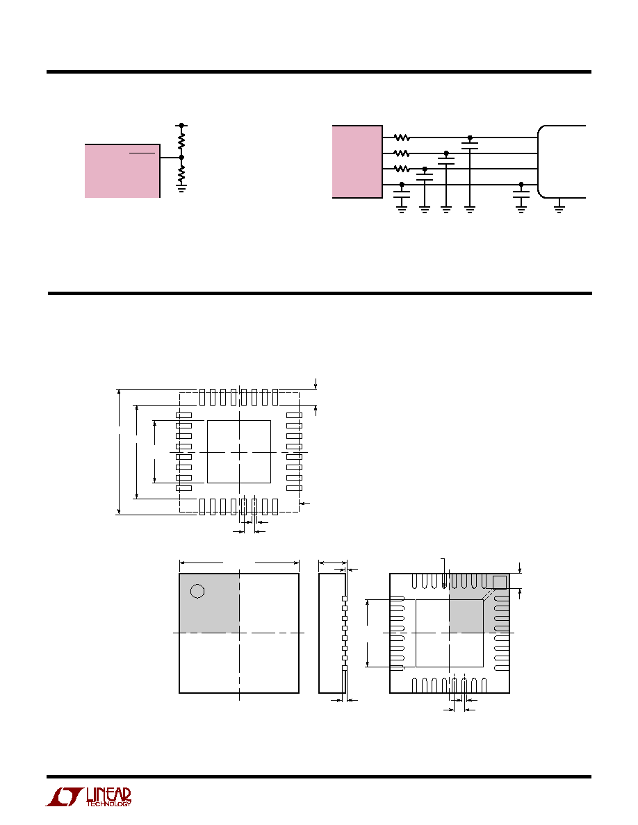
PACKAGE DESCRIPTIO
U
5.00
±
0.10
(4 SIDES)
NOTE:
1. DRAWING PROPOSED TO BE A JEDEC PACKAGE OUTLINE
M0-220 VARIATION WHHD-(X) (TO BE APPROVED)
2. DRAWING NOT TO SCALE
3. ALL DIMENSIONS ARE IN MILLIMETERS
4. DIMENSIONS OF EXPOSED PAD ON BOTTOM OF PACKAGE DO NOT INCLUDE
MOLD FLASH. MOLD FLASH, IF PRESENT, SHALL NOT EXCEED 0.20mm ON ANY SIDE
5. EXPOSED PAD SHALL BE SOLDER PLATED
PIN 1
TOP MARK
0.40
±
0.10
31
1
2
32
BOTTOM VIEW--EXPOSED PAD
3.45
±
0.10
(4-SIDES)
0.75
±
0.05
R = 0.115
TYP
0.23
±
0.05
(UH) QFN 0102
0.50 BSC
0.200 REF
0.00 ≠ 0.05
0.57
±
0.05
3.45
±
0.05
(4 SIDES)
4.20
±
0.05
5.35
±
0.05
0.23
±
0.05
PACKAGE OUTLINE
0.50 BSC
RECOMMENDED SOLDER PAD LAYOUT
UH Package
32-Lead Plastic QFN (5mm
◊
5mm)
(Reference LTC DWG # 05-08-1693)
Information furnished by Linear Technology Corporation is believed to be accurate and reliable.
However, no responsibility is assumed for its use. Linear Technology Corporation makes no represen-
tation that the interconnection of its circuits as described herein will not infringe on existing patent rights.
LTC1955
20
sn1955 1955fs
Linear Technology Corporation
1630 McCarthy Blvd., Milpitas, CA 95035-7417
(408) 432-1900
q
FAX: (408) 434-0507
q
www.linear.com
©
LINEAR TECHNOLOGY CORPORATION 2002
LT/TP 0303 2K ∑ PRINTED IN USA
RELATED PARTS
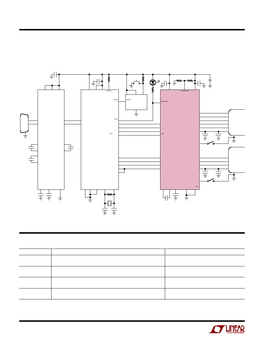
TYPICAL APPLICATIO
U
PART NUMBER
DESCRIPTION
COMMENTS
LTC1755/LTC1756
ISO 7816-3 and EMV Compatible Smart Card Interface
V
OUT
= 3V/5V, V
IN
= 2.7V to 6V,
SSOP-16/-24 Package
LTC1555
SIM Power Supply and Level Translator Step-Up/Step-Down Charge Pump
V
OUT
= 3V/5V, V
IN
= 2.7V to 10V,
SSOP-16/-20 Package
LTC1555L-1.8
SIM Power Supply and Level Translator Step-Up/Step-Down Charge Pump
V
OUT
= 1.8V/3V/5V, V
IN
= 2.6V to 6V,
SSOP-16 Package
LTC4555
SIM Power Supply and Level Translator
V
OUT
= 1.8V/3V, V
IN
= 3V to 6V, 3mm
◊
3mm
QFN Package
CARD A
CARD B
LTC1955EUH
1
µ
F
D
IN
DV
CC
V
CC
UNDERV
V
BATT
ASYNC
D
OUT
SYNC
SCLK
R
IN
LD
DATA
I/O B
RST B
CLK B
V
CCB
I/O A
C4A
C8A
RST A
CLK A
V
CCA
CPO
V
≠
GND
NC/NO
C
≠
11
14
15
C
+
FAULT
1955 TA02
24
23
1
4
12, 13
27
28
26
25
31
32
30
29
42
41
43
44
24
8
9
1
5
4
3
6
7
8
20
19
18
PRES B
PRES A
2
21
17
C7
C4
C8
C2
C3
C1
C7
C2
C3
C1
9, 10
22
4.7
µ
F
28
15
0.1
µ
F
V
+
1
5
0.1
µ
F
1
µ
F
1
µ
F
0.1
µ
F
0.1
µ
F
C5
C5
RD
TD
GND
DB9
0.1
µ
F
1k
0.1
µ
F
XIRQ
19
37
0.1
µ
F
180k
Li-ION
4.7
µ
F
262k
+
RST
2
1
36
V
CC18
4
5
V
CC3
3
V
CCA
GND
LTC1728ES5-1.8
DREN
17
RXEN
16
MOD B
21
V
DD
V
RH
45
22
26
27
18
20
XTAL
EXTAL
V
RL
V
SS
GND
MODA
47k
RST
47k
RESET
FAULT
(MOSI) PD3
38
IRQ
(2MHz) E
(MISO) PD2
25
24
40
39
DR1IN
RX1OUT
7
8
2
3
DR1OUT
RX1IN
PD1 (TXD)
PD0 (RXD)
PB1
(SCK) PD4
PB0
(SS) PD5
(IC3) PA0
28
PC0
0.1
µ
F
3
C2
≠
2
C2
+
0.1
µ
F
6
C1
≠
5
C1
+
0.1
µ
F
26
C3
≠
27
C3
+
10M
8.000MHz
27pF
27pF
MC68L11E9PB2
LTC1348CG
Battery Powered RS232 to Dual Smart Card Interface