Äîêóìåíòàöèÿ è îïèñàíèÿ www.docs.chipfind.ru
LTC1980
1
1980i
s
Digital Cameras
s
Handheld Computers
s
Personal Digital Assistants
s
1W to 10W Uninterruptable Power Supplies
Information furnished by Linear Technology Corporation is believed to be accurate and reliable.
However, no responsibility is assumed for its use. Linear Technology Corporation makes no represen-
tation that the interconnection of its circuits as described herein will not infringe on existing patent rights.
Final Electrical Specifications
APPLICATIO S
U
FEATURES
DESCRIPTIO
U
TYPICAL APPLICATIO
U
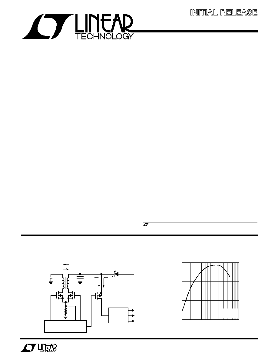
Combination Battery
Charger and DC/DC Converter
May 2003
The LTC
®
1980 integrates PWM power control for charg-
ing a battery and converting the battery voltage to a
regulated output or simultaneously charging the battery
while powering system load from an unregulated AC wall
adapter. Combining these features into a single IC pro-
duces a smaller area and lower cost solution compared to
presently available multi-IC solutions. The LTC1980 shares
the discrete components for both the battery charger and
the DC/DC converter thus minimizing size and cost relative
to dual controller solutions. Both the battery charger and
DC/DC converter use a current mode flyback topology for
high efficiency and excellent transient response. Optional
Burst Mode operation and power-down mode allow power
density, efficiency and output ripple to be tailored to the
application.
The LTC1980 provides a complete Li-Ion battery charger
with charge termination timer, preset Li-Ion battery volt-
ages, overvoltage and undervoltage protection, and user-
programmable constant-current charging. Automatic bat-
tery recharging, shorted-cell detection, and open-drain
C/10 and wall plug detect outputs are also provided. User
programming allows NiMH and NiCd battery chemistries
to be charged as well.
s
Single Controller IC Includes Battery Charger
Plus DC/DC Converter
s
Wall Adapter Voltage May be Above or Below
Battery Voltage
s
LDO Controller Allows Simultaneous Charging
and Regulating from Wall Adapter Input
s
Standalone Li-Ion Battery Charger Including Charge
Termination, Overvoltage Protection, Shorted-Cell
Detection and Battery Recharge
s
Selectable 4.1V, 4.2V, 8.2V and 8.4V Float Voltages
s
Simple NiMH and NiCd Battery Charger
s
Pin Programmable Regulator Burst Mode
®
Operation
and Shutdown for High Efficiency
s
High Efficiency Current Mode 300kHz PWM
s
Reduced Component Architecture
s
Undervoltage Protection and Soft-Start Insures
Start-Up with Current Limited Wall Adapter
s
Small 24-Pin SSOP Package
, LTC and LT are registered trademarks of Linear Technology Corporation.
Burst Mode is a registered trademark of Linear Technology Corporation.
LTC1980
·
·
Li-Ion
BATTERY
POWER FLOW
CHARGING
BATTERY
OPERATION
SYSTEM
POWER
LDO/
SWITCH
3.3V
UNREGULATED
WALL ADAPTER
INPUT (3V TO 10V)
1.8V
1.5V
1980 TA01
SYSTEM LOAD
DC/DC
CONVERTERS
BAT-FET
REG-FET
Li-Ion Charger and DC/DC Converter Using One IC
LOAD CURRENT (mA)
10
EFFICIENCY (%)
90
85
80
75
70
65
60
100
1000
1980 G04
V
BAT
= 3.6V
T
A
= 25
°
C
FIGURE 5
3.3V Regulator Efficiency vs Load Current
LTC1980
2
1980i
ABSOLUTE AXI U RATI GS
W
W
W
U
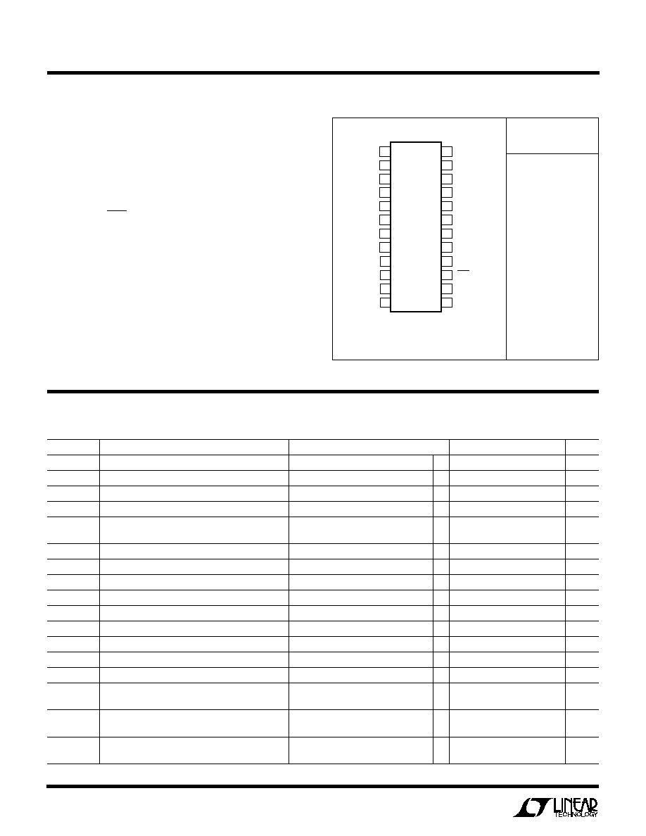
PACKAGE/ORDER I FOR ATIO
U
U
W
V
REG
to GND ............................................. 0.5V to 12V
V
BAT
to GND ............................................. 0.5V to 12V
PROG, I
SENSE
.............................................. 0.5V to 5V
PROGT, REGFB, V
C
, BATT1, BATT2
TIMER, SS ............................................ 0.5V to V
BIAS2
LDOFB, LDODRV .................................... 0.5V to V
REG
WA, V
BIAS1
, REG ....................................... 0.5V to 12V
MODE ................................................... 0.5V to V
BIAS1
V
BIAS2
......................................................... 0.5V to 5V
OVP ............................................................ 0.5V to 5V
PGND to GND .................................... Connect Together
Operating Ambient Temperature Range
(Note 2) ................................................. 40
°
C to 85
°
C
Storage Temperature Range ................. 65
°
C to 125
°
C
Lead Temperature (Soldering, 10 sec)................ 300
°
C
(Note 1)
ORDER PART
NUMBER
1
2
3
4
5
6
7
8
9
10
11
12
TOP VIEW
GN PACKAGE
24-LEAD NARROW PLASTIC SSOP
24
23
22
21
20
19
18
17
16
15
14
13
SS
OVP
CAOUT
I
SENSE
GND
V
BIAS2
V
BAT
TIMER
MODE
REG
BGTDR
V
BIAS1
PROG
PROGT
REGFB
V
C
LDOFB
LDODRV
V
REG
WA
BATT1
BATT2
RGTDR
PGND
LTC1980EGN
T
JMAX
= 125
°
C,
JA
= 85
°
C/W
Consult LTC Marketing for parts specified with wider operating temperature ranges.
ELECTRICAL CHARACTERISTICS
SYMBOL
PARAMETER
CONDITIONS
MIN
TYP
MAX
UNITS
V
BAT
Positive Supply Voltage, V
BAT
2.85
10
V
V
REG
Positive Supply Voltage, V
REG
2.85
10
V
V
FB
Feedback Voltage
REGFB Tied to V
C
q
1.194
1.225
1.256
V
V
PROGT
Voltage on PROGT Pin
PROGT Tied to V
C
1.194
1.225
1.256
V
I
BURST
Burst Mode Operation
Regulator Mode, REGFB = 1.5V
0.75
mA
Supply Current, Quiescent, V
REG
I
HIGH
Supply Current, Quiescent, V
REG
Regulator Mode, REGFB = 0V
q
2
4.3
mA
I
SHDN
Supply Current in Shutdown Mode, V
REG
Mode = 0V
15
µ
A
V
UVL
Positive-Going Undervoltage Lockout Voltage
From Either V
BAT
or V
REG
2.45
2.7
2.85
V
V
UVHYS
Undervoltage Lockout Hysteresis
From Either V
BAT
or V
REG
100
mV
I
SS
Soft-Start Ramp Current
BATT1 = 0, BATT2 = 0, Charger Mode
10
µ
A
V
FLOAT0
Output Float Voltage in Constant Voltage Mode
BATT1 = 0, BATT2 = 0
q
4.059
4.1
4.141
V
V
FLOAT1
Output Float Voltage in Constant Voltage Mode
BATT1 = 0, BATT2 = 0
q
4.158
4.2
4.242
V
V
FLOAT2
Output Float Voltage in Constant Voltage Mode
BATT1 = 0, BATT2 = 1 (Note 3)
q
8.118
8.2
8.282
V
V
FLOAT3
Output Float Voltage in Constant Voltage Mode
BATT1 = 0, BATT2 = 1 (Note 3)
q
8.316
8.4
8.484
V
V
FLOAT4
Output Float Voltage in Constant Voltage Mode
BATT1 = Open, BATT2 = Don't Care
q
1.207
1.225
1.243
V
Measured from OVP Input
V
RCHG0
Recharge Threshold, Delta Voltage with Respect
BATT2 = 0, BATT1 = 0 or 1
200
mV
to Float Voltage
V
RCHG1
Recharge Threshold, Delta Voltage with Respect
BATT2 = 1, BATT1 = 0 or 1
400
mV
to Float Voltage
The
q
denotes the specifications which apply over the full operating
temperature range, otherwise specifications are at T
A
= 25
°
C. V
BAT
= 2.4V, V
REG
= 5V, V
BAT
unloaded.
LTC1980
3
1980i
ELECTRICAL CHARACTERISTICS
SYMBOL
PARAMETER
CONDITIONS
MIN
TYP
MAX
UNITS
V
RCHG2
Recharge Threshold, Delta Voltage with Respect
BATT 1 = Open
60
mV
to Float Voltage, Measured at OVP
V
LT0
Charger Shorted Cell Threshold
BATT2 = 0
2.55
2.7
2.8
V
V
LT1
Charger Shorted Cell Threshold
BATT2 = 1
5.2
5.4
5.65
V
I
BLDO
Input Bias Current, Low Dropout Regulator
Measured at LDOFB Pin
1.0
µ
A
g
mldo
Transconductance, Low Dropout Regulator
Measured from LDOFB to LDODRV
350
µ
mhos
V
OLLDO
Output Low Voltage, Low Dropout Regulator
0.1
V
V
OHLDO
Output High Voltage, Low Dropout Regulator
V
REG
0.1
V
I
OUTLDO
Low Dropout Regulator Output Current, Source/Sink
±
20
µ
A
A
VOL
Error Amplifier Open-Loop Voltage Gain
From REGFB to V
C
60
dB
I
BEA
Error Amplifier Input Bias Current
0.1
0.1
µ
A
V
OLEA
Error Amplifier Output Low Voltage
0
0.5
V
V
OHEA
Error Amplifier Output High Voltage
SS = Open
1.4
2
V
I
OUT
Error Amplifier Output Source Current
0.5
mA
Error Amplifier Output Sink Current
1.2
mA
g
mflt
Float Voltage Error Amplifier Transconductance
Measured from OVP to SS,
65
µ
mhos
Charger Mode, BATT1 = Open
I
BFLT
Float Voltage Error Amplifier Input Current
0.1
0.1
µ
A
(Measured at OVP Input)
V
OS1
Current Amplifier Offset Voltage
6
6
mV
I
BIS
Input Bias Current, I
SENSE
Input
100
µ
A
A
VCA
Current Amplifier Voltage Gain
Measured from I
SENSE
to
2.3
2.44
2.55
V/V
CAOUT Pin
R
PROG
PROG Pin On Resistance
400
I
PROG
PROG Pin Leakage Current
100
nA
f
S
Switching Frequency
q
260
300
340
kHz
t
r
, t
f
Driver Output Transition Times
C
L
= 15pF
10
ns
t
BREAK
Driver Output Break Times
V
BAT
= V
REG
= 10V
100
ns
f
TIMER
Timer Frequency
C = 1000pF
4.5
kHz
I
TIMER1
TIMER Pin Source Current
4
µ
A
I
TIMER2
TIMER Pin Sink Current
4
µ
A
R
REG
REG On Resistance
68
I
REGPD
REG Pull-Down Current
2
5
9
µ
A
I
REGLK
REG Leakage Current
60
nA
V
VTHREG
REG Logic Threshold
0.3
1.3
V
V
IL1
Digital Input Low Voltage,
V
REG
= 5V
1.185
1.221
1.247
V
Negative-Going, Wall Adapter (WA)
V
IH1
Digital Input High Voltage,
V
REG
= 5V
1.195
1.226
1.257
V
Positive-Going, Wall Adapter (WA)
V
IL2
Digital Input Low Voltage, BATT1
100
mV
V
IH2
Digital Input High Voltage, BATT1
V
BIAS2
V
100mV
The
q
denotes the specifications which apply over the full operating
temperature range, otherwise specifications are at T
A
= 25
°
C. V
BAT
= 2.4V, V
REG
= 5V, V
BAT
unloaded.
LTC1980
4
1980i
ELECTRICAL CHARACTERISTICS
The
q
denotes the specifications which apply over the full operating
temperature range, otherwise specifications are at T
A
= 25
°
C.V
BAT
= 2.4V, V
REG
= 5V, V
BAT
unloaded.
SYMBOL
PARAMETER
CONDITIONS
MIN
TYP
MAX
UNITS
V
P2
Digital Input Pull-Up Voltage, BATT1
BATT1 Input Floating
1.6
V
V
IL3
Digital Input Low Voltage, BATT2
0.3
V
V
IH3
Digital Input High Voltage, BATT2
2
V
I
I1
Digital Input Current, WA
5
5
µ
A
I
I2
Digital Input Current, BATT1
10
10
µ
A
I
I3
Digital Input Current, BATT2
1
1
µ
A
Note 1: Absolute Maximum Ratings are those values beyond which the life
of a device may be impaired.
Note 2: The LTC1980E is guaranteed to meet performance specifications
from 0
°
C to 70
°
C. Specifications over the 40
°
C to 85
°
C operating
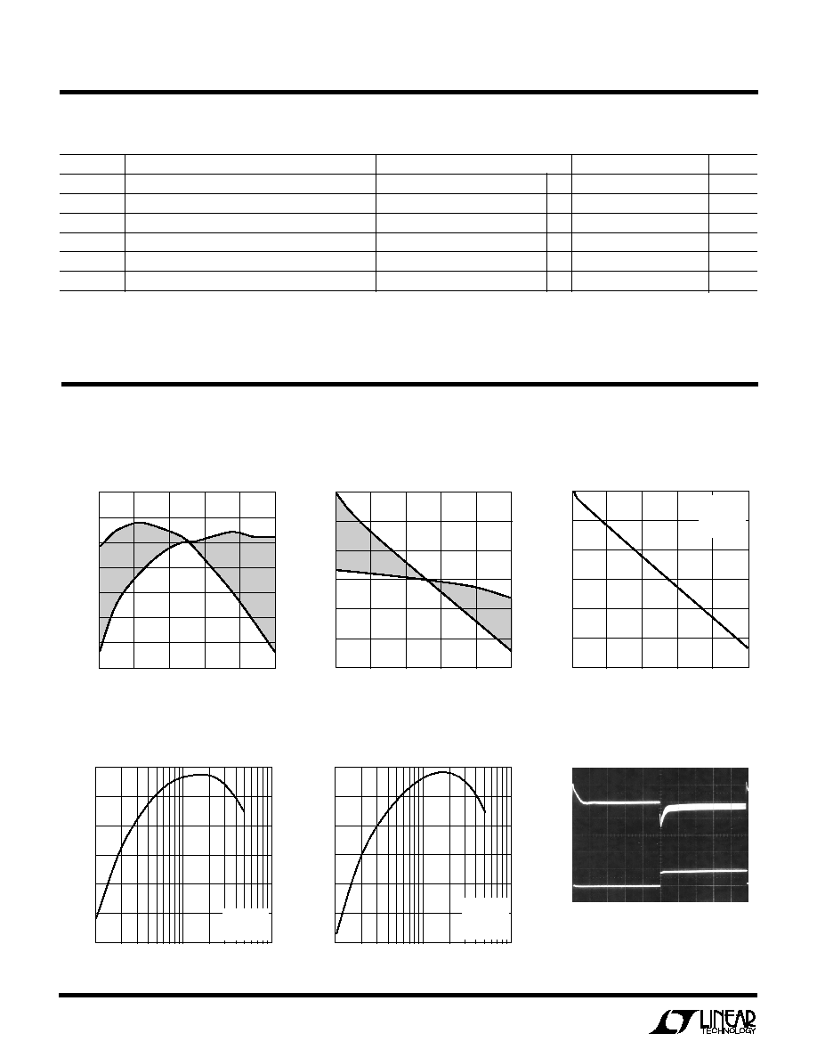
Feedback Reference Voltage
vs Temperature
Switching Frequency Variance
vs Temperature
Regulator Load Regulation
3.3V Regulator Efficiency
vs Load Current
5V Regulator Efficiency
vs Load Current
Regulator Load Step Response
TYPICAL PERFOR A CE CHARACTERISTICS
U
W
temperature range are assured by design, characterization and correlation
with statistical process controls.
Note 3: T
A
= 0
°
C to 70
°
C.
TEMPERATURE (
°
C)
FEEDBACK REFERENCE VOLTAGE (V)
1980 G01
1.2240
1.2235
1.2230
1.2225
1.2220
1.2215
1.2210
1.2205
40
15
10
35
60
85
TEMPERATURE (
°
C)
FREQUENCY VARIANCE (%)
1980 G02
1.5
1.0
0.5
0
0.5
1.0
1.5
40
15
10
35
60
85
LOAD CURRENT (mA)
0
V
REG
(%)
0
0.2
0.4
0.6
0.8
1.0
1.2
100
200
300
400
1980 G03
500
V
BAT
= 4.2V
V
REG
3.3V
T
A
= 25
°
C
FIGURE 5
LOAD CURRENT (mA)
10
EFFICIENCY (%)
90
85
80
75
70
65
60
100
1000
1980 G04
V
BAT
= 3.6V
T
A
= 25
°
C
FIGURE 5
LOAD CURRENT (mA)
10
EFFICIENCY (%)
90
85
80
75
70
65
60
100
1000
1980 G05
V
BAT
= 3.6V
T
A
= 25
°
C
R8 = 309k
FIGURE 5
V
REG
50mV/DIV
100
µ
s/DIV
I
L
500mA/DIV
V
BAT
= 3.6V
V
REG
3.3V
I
L
= 100mA TO 500mA
T
A
= 25
°
C
FIGURE 5
1980 G06
LTC1980
5
1980i
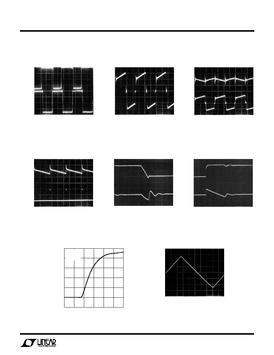
Typical BGTDR and RGTDR
Waveforms
Typical I
SENSE
Waveforms,
Regulator
Typical Operation with Burst
Mode Operation Disabled
TYPICAL PERFOR A CE CHARACTERISTICS
U
W
Burst Mode Circuit Operation
Regulator Output Transient
Response--Wall Adapter Removal
Mode Pin Input Current vs V
IN
Typical C
TIMER
Waveform
Regulator Output Transient
Response--Wall Adapter "Hot
Plugged"
BGTDR
1V/DIV
1
µ
s/DIV
RGTDR
1V/DIV
V
BAT
= 3.6V
V
REG
= 3.3V
T
A
= 25
°
C
I
L
= 500mA
1980 G07
I
SENSE
20mV/DIV
PIN 21
FIGURE 5
1
µ
s/DIV
V
BAT
= 3.6V
V
REG
= 3.3V
I
L
= 500mA
T
A
= 25
°
C
FIGURE 5
1980 G08
V
REG
50mV/DIV
1
µ
s/DIV
I
SENSE
50mV/DIV
V
BAT
= 3.6V
V
REG
3.3V
I
L
= 500mA
MODE = V
BIAS1
T
A
= 25
°
C
FIGURE 5
1980 G09
V
REG
50mV/DIV
200
µ
s/DIV
BGTDR
2V/DIV
V
BAT
= 3.6V
V
REG
= 3.3V
I
L
= 10mA
T
A
= 25
°
C
FIGURE 5
1980 G10
MODE PIN V
IN
(V)
0
MODE PIN INPUT CURRENT (
µ
A)
1.5
1.0
0.5
0
0.5
1.0
1.5
0.5
1.0
1.5
2.0
1980 G13
2.5
3.0
V
BAT
= 2.4V
V
REG
= 5V
T
A
= 25
°
C
V
REG
1V/DIV
500
µ
s/DIV
V
LDO
0.1V/DIV
V
BAT
= 3.6V
V
REG
= 3.3V
V
LDO
= 3.1V
I
LDO
= 200mA
V
WALL ADAPTER
= 6V TO 0V
T
A
= 25
°
C
FIGURE 5
1980 G11
V
REG
1V/DIV
500
µ
s/DIV
V
LDO
0.5V/DIV
V
BAT
= 3.6V
V
REG
= 3.3V
V
LDO
= 3.1V
I
LDO
= 200mA
V
WALL ADAPTER
= 0V TO 6V
T
A
= 25
°
C
FIGURE 5
1980 G12
TIMER
100mV/DIV
PIN 17
5ms/DIV
C
TIMER
= 0.24
µ
F
T
A
= 25
°
C
1980 G14