
LTC1983-3/LTC1983-5
1
sn1983 1983fs
The LTC
Æ
1983-3 and LTC1983-5 are inverting charge
pump DC/DC converters that produce negative regulated
outputs. The parts require only three tiny external capaci-
tors and can provide up to 100mA of output current. The
devices can operate in open loop mode (creating a ≠V
IN
supply) or regulated output mode depending on the input
supply voltage and the output current.
The LTC1983-3/LTC1983-5 have many useful features for
portable applications including very low quiescent current
(25
µ
A typical) and a zero current shutdown mode pro-
grammed through the SHDN pin.
The LTC1983-3/LTC1983-5 are over-temperature and
short-circuit protected. The parts are available in a 6-pin
low profile (1mm) ThinSOT package.
s
≠3V Generation in Single-Supply Systems
s
Portable Equipment
s
LCD Bias Supplies
s
GaAs FET Bias Supplies
s
Fixed Output Voltages: ≠3V, ≠5V or Low Noise V
IN
to ≠V
IN
Inverted Output
s
±
4% Output Voltage Accuracy
s
Low Quiesient Current: 25
µ
A
s
100mA Output Current Capability
s
3V to 5.5V Operating Voltage Range (LTC1983-3)
s
2.3V to 5.5V Operating Voltage Range (LTC1983-5)
s
Internal 900kHz Oscillator
s
"Zero Current" Shutdown
s
Short-Circuit and Over-Temperature Protected
s
Low Profile (1mm) ThinSOT
TM
Package
100mA Regulated
Charge-Pump Inverters
in ThinSOT
, LTC and LT are registered trademarks of Linear Technology Corporation.
ThinSOT is a trademark of Linear Technology Corporation.
V
IN
SHDN
C
+
V
OUT
GND
C
≠
LTC1983-3
V
IN
3V TO 5.5V
V
OUT
= ≠3V
I
OUT
= UP TO 100mA
C
OUT
10
µ
F
C
IN
10
µ
F
C
FLY
1
µ
F
OFF ON
C
FLY
: TAIYO YUDEN LMK212BJ105
C
IN
, C
OUT
: TAIYO YUDEN JMK316BJ106ML
1983-3 TA01
V
OUT
vs I
OUT
I
OUT
(mA)
0
V
OUT
(V)
≠3.3
≠3.2
≠3.1
≠3.0
≠2.9
≠2.8
≠2.7
20
40
60
80
1983 TA02
100
V
IN
= 5V
V
IN
= 3.3V
DESCRIPTIO
U
FEATURES
APPLICATIO S
U
TYPICAL APPLICATIO
U
≠3V at 100mA DC/DC Converter
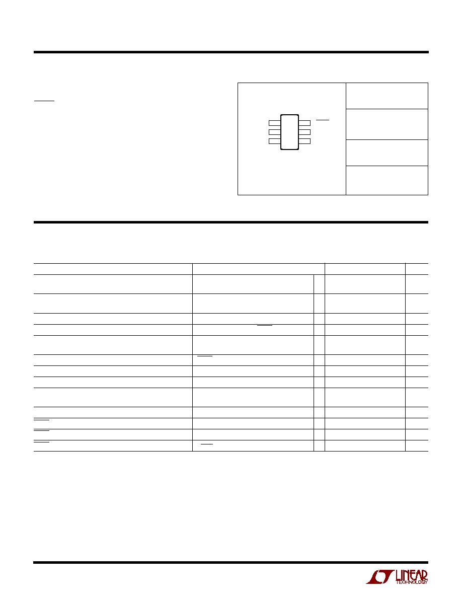
LTC1983-3/LTC1983-5
2
sn1983 1983fs
V
IN
to GND ................................................... ≠0.3V to 6V
SHDN Voltage .............................................. ≠0.3V to 6V
V
OUT
to GND (LTC1983-3) .................. 0.2V to V
OUT
Max
V
OUT
to GND (LTC1983-5) .................. 0.2V to V
OUT
Max
I
OUT
Max ............................................................. 125mA
Output Short-Circuit Duration .......................... Indefinite
Operating Temperature Range (Note 2) ...≠40
∞
C to 85
∞
C
Storage Temperature Range ................. ≠ 65
∞
C to 125
∞
C
Lead Temperature (Soldering, 10 sec).................. 300
∞
C
ORDER PART
NUMBER
S6 PART
MARKING
T
JMAX
= 125
∞
C,
JA
= 256
∞
C/W
Consult LTC Marketing for parts specified with wider operating temperature ranges.
LTPC
LTYB
LTC1983ES6-3
LTC1983ES6-5
ABSOLUTE AXI U
RATI GS
W
W
W
U
PACKAGE/ORDER I FOR ATIO
U
U
W
(Note 1)
ELECTRICAL CHARACTERISTICS
Burst Mode is a registered trademark of Linear Technology
Corporation.
Note 1: Absolute Maximum Ratings are those values beyond
which the life of a device may be impaired.
The
q
denotes the specifications which apply over the full operating
temperature range, otherwise specifications are at T
A
= 25
∞
C. V
IN
= 5V, C
FLY
= 1
µ
F, C
OUT
= 10
µ
F
unless otherwise noted.
PARAMETER
CONDITIONS
MIN
TYP
MAX
UNITS
V
IN
Operating Voltage (Regulated Output Mode) (LTC1983-3)
q
3.0
5.5
V
V
IN
Min Startup Voltage
2.3
V
V
OUT
(LTC1983-3)
V
IN
3.3V, I
OUT
25mA
q
≠2.88
≠3
≠3.12
V
V
IN
5V, I
OUT
100mA
q
≠2.88
≠3
≠3.12
V
V
OUT
(LTC1983-5)
V
IN
5V, V
IN
≠5V
I
OUT
∑ R
OUT
q
≠ 4.8
≠5
≠ 5.2
V
V
IN
Operating Current
V
IN
5.5V, I
OUT
= 0
µ
A, SHDN = V
IN
q
25
60
µ
A
V
IN
Operating Current (Open-Loop Mode) (LTC1983-5)
V
IN
= 3.3V
2.5
mA
V
IN
= 4.75V
4
mA
V
IN
Shutdown Current
SHDN = 0V, V
IN
5.5V
q
0.1
1
µ
A
Output Ripple
3.3
V
IN
5.5
60
mV
P-P
Open-Loop Output Impedance (LTC1983-3): R
OUT
V
IN
= 3.3V, V
OUT
= ≠3V
11
Open-Loop Output Impedance (LTC1983-5): R
OUT
V
IN
= 3.3V, I
OUT
50mA
11
V
IN
= 5V, I
OUT
60mA
8.5
Oscillator Frequency
(Non-Burst Mode
Æ
Operation)
900
kHz
SHDN Input High
q
1.1
V
SHDN Input Low
q
0.3
V
SHDN Input Current
V
SHDN
= 5.5V
q
2.2
4
µ
A
V
CC
1
V
OUT
2
C
+
3
6 SHDN
5 GND
4 C
≠
TOP VIEW
S6 PACKAGE
6-LEAD PLASTIC SOT-23
Note 2: The LTC1983E-3/LTC1983E-5 are guaranteed to meet
performance specifications from 0
∞
C to 70
∞
C. Specifications over the
≠ 40
∞
C to 85
∞
C operating temperature range are assured by design,
characterization and correlation with statistical process controls.
LTC1983-3/LTC1983-5
3
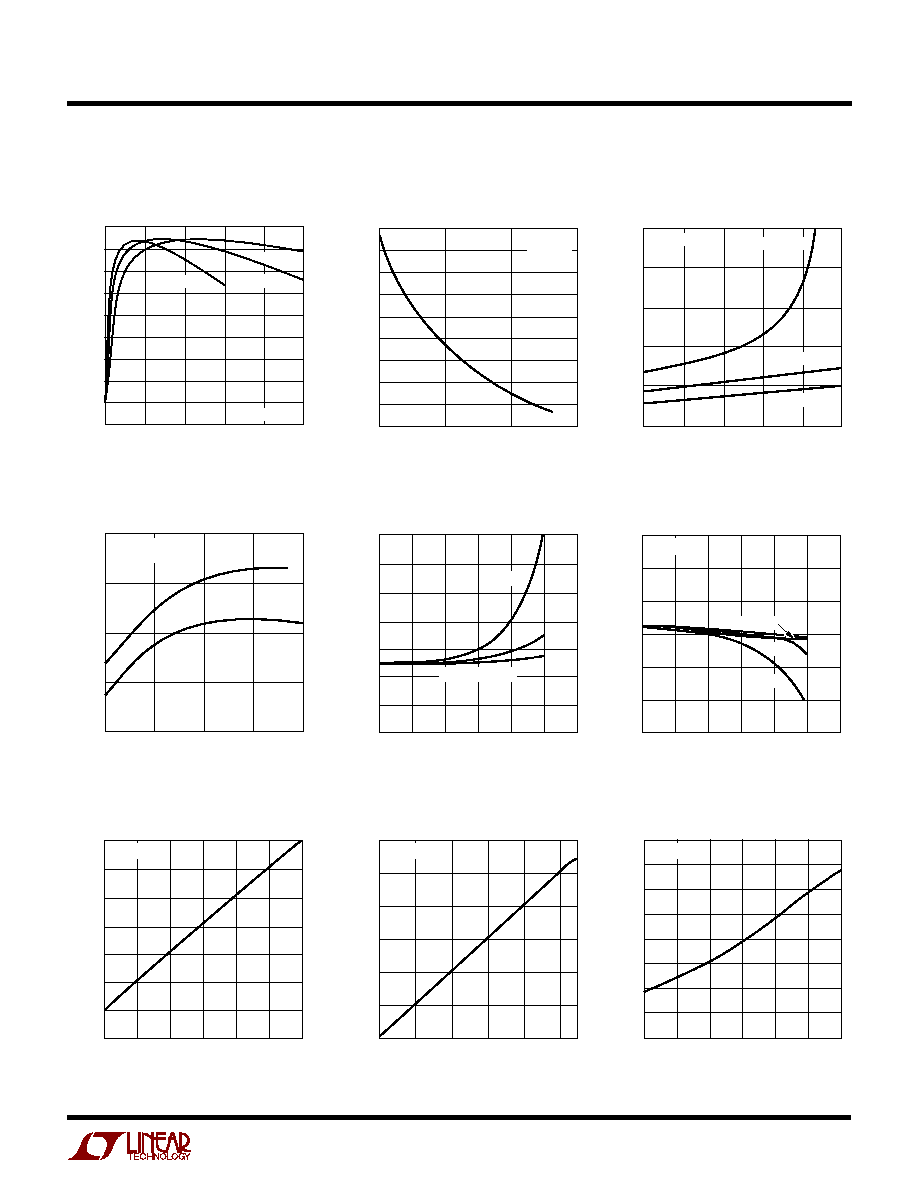
sn1983 1983fs
Output Impedance vs
Input Voltage
Output Impedance
vs I
OUT
(LTC1983-5)
Efficiency vs I
OUT
(LTC1983-5)
TYPICAL PERFOR A CE CHARACTERISTICS
U
W
Efficiency vs I
OUT
I
OUT
(mA)
0
EFFICIENCY (%)
40
80
100
90
80
70
60
50
40
30
20
10
0
1983 G01
20
60
V
IN
= 2.3V
V
IN
= 3.3V
V
IN
= 5V
T
A
= 25
∞
C
V
IN
(V)
2.35
R
OUT
(
)
4.35
12.5
12.0
11.5
11.0
10.5
10.0
9.5
9.0
8.5
8.0
1983 TA02
3.35
5.35
R
OUT
I
OUT
= 25mA
T
A
= 25
∞
C
I
OUT
(mA)
0
R
OUT
(
)
40
80
100
30
25
20
15
10
5
1983 G03
20
60
V
IN
= 2.3V
V
IN
= 3.3V
V
IN
= 5V
T
A
= 25
∞
C
I
OUT
(mA)
0.01
100
75
50
25
0
10
1983 GO4
0.1
1
100
EFFICIENCY (%)
V
IN
= 5V
V
IN
= 3.3V
V
OUT
= ≠3V
T
A
= 25
∞
C
OUTPUT CURRENT (mA)
0
≠2.1
≠2.3
≠2.5
≠2.7
≠2.9
≠3.1
≠3.3
≠3.5
60
100
1983 G05
20
40
80
120
V
OUT
(V)
120
∞
C
≠40
∞
C, 0
∞
C, 40
∞
C
80
∞
C
OUTPUT CURRENT (mA)
0
2.7
V
OUT
(≠
V)
2.8
2.9
3.0
3.1
3.3
20
40
60
80
1983 G06
100
120
3.2
≠40
∞
C 0
∞
C
40
∞
C
80
∞
C
V
IN
= 5V
≠3V
OUT
vs I
OUT
Over Temperature
≠3V
OUT
vs I
OUT
Over Temperature
(V
IN
= 5V)
Open-Loop Current
vs Temperature (LTC1983-5)
TEMPERATURE (
∞
C)
≠40
4.9
4.7
4.5
4.3
4.1
3.9
3.7
3.5
1983 G07
10
60
110
I
IN
(mA)
V
IN
= 5V
Burst Mode Current
vs Temperature (LTC1983-3)
TEMPERATURE (
∞
C)
≠40
I
IN
(
µ
A)
25
30
35
1983 G08
20
15
10
10
60
40
45
50
110
V
IN
= 5V
Open-Loop Input Current
vs V
IN
(LTC1983-5)
V
IN
(V)
2.3
1.5
I
IN
(mA)
2.0
2.5
3.0
3.5
4.5
2.8
3.3
3.3
4.3
1983 G09
4.8
4.0
T
A
= 25
∞
C
LTC1983-3/LTC1983-5
4
sn1983 1983fs
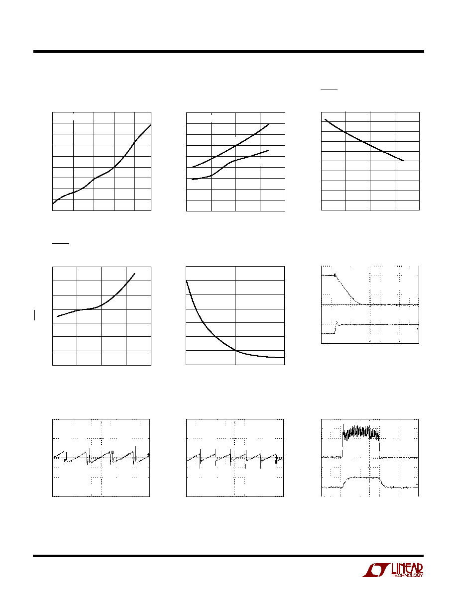
TYPICAL PERFOR A CE CHARACTERISTICS
U
W
Burst Mode Input Current
vs V
IN
(LTC1983-3)
V
IN
(V)
3.1
26.5
INPUT CURRENT (
µ
A)
27.0
28.0
28.5
29.0
4.1
5.1
5.5
31.0
1983 G10
27.5
3.6
4.6
29.5
30.0
30.5
T
A
= 25
∞
C
TEMPERATURE (
∞
C)
≠50
R
OUT
(
)
10
12
14
150
1983 G11
8
6
0
0
50
100
4
2
18
16
V
IN
= 5V
V
IN
= 3V
I
OUT
= 10mA
TEMPERATURE (
∞
C)
≠50
0
V
THRESHOLD
(V)
0.1
0.3
0.4
0.5
1.0
0.7
0
50
1983 G12
0.2
0.8
0.9
0.6
100
150
R
OUT
vs Temperature
(I
OUT
= 10mA)
SHDN Pin Threshold Voltage
vs Temperature
SHDN Pin Input Current
vs Temperature
R
OUT
vs C
FLY
(V
IN
= 5V)
TEMPERATURE (
∞
C)
≠50
2.0
2.5
3.5
100
1983 G13
1.5
1.0
0
50
150
0.5
0
3.0
I
SHDN
C
FLY
(
µ
F)
0.01
1400
V
IN
= 5V
T
A
= 25
∞
C
1200
1000
800
600
400
200
1983 G14
0.1
1
0
R
OUT
(
)
V
OUT
Start-Up into 100mA
Resistive Load
V
OUT
Ripple at 100mA Load
V
OUT
Ripple at 30mA Load
V
OUT
Load Step Reponse from
I
OUT
= 0 to I
OUT
= 100mA
V
OUT
1V
V
IN
5V
V
OUT
20mV
50
µ
s/DIV
1983 G15
1
µ
s/DIV
1983 G16
V
OUT
20mV
2.5
µ
s/DIV
1983 G17
V
OUT
20mV
100
µ
s/DIV
1983 G18
I
OUT
100mA
LTC1983-3/LTC1983-5
5
sn1983 1983fs
U
U
U
PI FU CTIO S
V
IN
(Pin 1): Charge Pump Input Voltage. May be between
2.3V and 5.5V. V
IN
should be bypassed with a
4.7
µ
F low
ESR capacitor as close as possible to the pin for best
performance.
V
OUT
(Pin 2): Regulated Output Voltage for the IC. V
OUT
should be bypassed with a
4.7
µ
F low ESR capacitor as
close as possible to the pin for best performance.
C
+
(Pin 3): Charge Pump Flying Capacitor Positive Termi-
nal. This node is switched between V
IN
and GND (It is
connected to V
CC
during shutdown).
C
≠
(Pin 4): Charge Pump Flying Capacitor Negative Termi-
nal. This node is switched between GND and V
OUT
(It is
connected to GND during shutdown).
GND (Pin 5): Signal and Power Ground for the 6-Pin
SOT-23 package. This pin should be tied to a ground plane
for best performance.
SHDN (Pin 6): Shutdown. Grounding this pin shuts down
the IC. Tie to V
IN
to enable. This pin should not be pulled
above the V
IN
voltage or below GND.
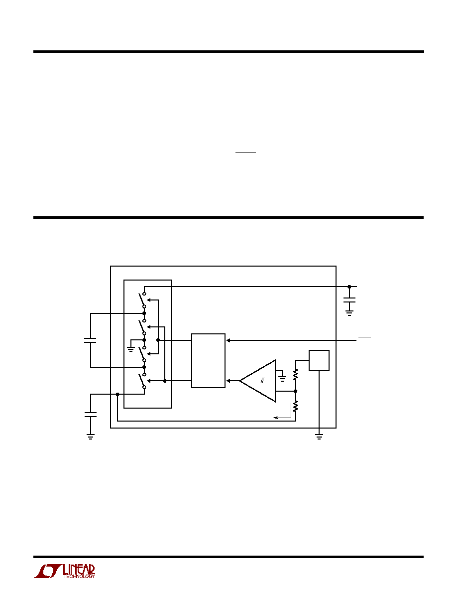
BLOCK DIAGRA
W
CONTROL
LOGIC
CLOCK2
CLOCK1
S1A
S2A
S1B
S2B
≠
+
V
REF
CHARGE PUMP
SHDN
V
IN
C
IN
10
µ
F
C
FLY
1
µ
F
C
OUT
10
µ
F
LTC1983-X
C
+
C
≠
V
OUT
COMP1
1
µ
A
1983 BD
LTC1983-3/LTC1983-5
6
sn1983 1983fs
OPERATIO
U
The LTC1983-3/LTC1983-5 use a switched capacitor
charge pump to invert a positive input voltage to a regu-
lated ≠3V
±
4% (LTC1983-3) or ≠5
±
4% (LTC1983-5)
output voltage. Regulation is achieved by sensing the
output voltage through an internal resistor divider and
enabling the charge pump when the output voltage droops
above the upper trip point of COMP1. When the charge
pump is enabled, a 2-phase, nonoverlapping clock con-
trols the charge pump switches. Clock 1 closes the S1
switches which enables the flying capacitor to charge up
to the V
IN
voltage. Clock 2 closes the S2 switches that
invert the V
IN
voltage and connect the bottom plate of C
FLY
to the output capacitor at V
OUT
. This sequence of charging
and discharging continues at a free-running frequency of
900kHz (typ) until the output voltage has been pumped
down to the lower trip point of COMP1 and the charge
pump is disabled. When the charge pump is disabled, the
LTC1983 draws only 25
µ
A (typ) from V
IN
which provides
high efficiency at low load conditions.
In shutdown mode, all circuitry is turned off and the part
draws less than 1
µ
A from the V
IN
supply. V
OUT
is also
disconnected from V
IN
and C
FLY
. The SHDN pin has a
threshold of approximately 0.7V. The part enters shut-
down when a low is applied to the SHDN pin . The SHDN
pin should not be floated; it must be driven with a logic
high or low.
Open-Loop Operation
The LTC1983-3/LTC1983-5 inverting charge pumps regu-
late at ≠3V/≠5V respectively, unless the input voltage is too
low or the output current is too high. The equations for
output voltage regulation are as follows:
V
IN
≠5.06V > I
OUT
∑ R
OUT
(LTC1983-5)
V
IN
≠3.06V > I
OUT
∑ R
OUT
(LTC1983-3)
If this condition is not met, then the part will run in open
loop mode and act as a low output impedance inverter for
which the output voltage will be:
V
OUT
= ≠[V
IN
≠(I
OUT
∑ R
OUT
)]
For all R
OUT
values, check the corresponding curves in
the Typical Performance Characteristics section (Note:
C
FLY
= 1
µ
F for all R
OUT
curves). The R
OUT
value will be
different for different flying caps, as shown in the follow-
ing equation:
R
R
curve
f
C
OUT
OUT
OSC
FLY
=
+
(
) ≠ .
∑
1 11
1
Short-Circuit/Thermal Protection
During short-circuit conditions, the LTC1983 will draw
several hundred milliamps from V
IN
causing a rise in the
junction temperature. On-chip thermal shutdown cir-
cuitry disables the charge pump once the junction tem-
perature exceeds
155
∞
C, and reenables the charge pump
once the junction temperature falls back to
145
∞
C. The
LTC1983 will cycle in and out of thermal shutdown
indefinitely without latchup or damage until the V
OUT
short is removed.
Capacitor Selection
For best performance, it is recommended that low ESR
capacitors be used for both C
IN
and C
OUT
to reduce noise
and ripple. The C
IN
and C
OUT
capacitors should be either
ceramic or tantalum and should be 4.7
µ
F or greater.
Aluminum electrolytic are not recommended because of
their high equivalent series resistance (ESR). If the source
impedance is very low, C
IN
may not be needed. Increasing
the size of C
OUT
to 10
µ
F or greater will reduce output
voltage ripple. The flying capacitor and C
OUT
should also
have low equivalent series inductance (ESL). The board
layout is critical as well for inductance for the same reason
(the suggested board layout should be used).
A ceramic capacitor is recommended for the flying capaci-
tor with a value in the range of 0.1
µ
F to 4.7
µ
F. Note that
a large value flying cap (>1
µ
F) will increase output ripple
unless C
OUT
is also increased. For very low load applica-
tions, C1 may be reduced to 0.01
µ
F to 0.047
µ
F. This will
reduce output ripple at the expense of efficiency and
maximum output current.
(Refer to Block Diagram)

LTC1983-3/LTC1983-5
7
sn1983 1983fs
There are many aspects of the capacitors that must be
taken into account. First, the temperature stability of the
dielectric is a main concern. For ceramic capacitors, a
three character code specifies the temperature stability
(e.g. X7R, Y5V, etc.). The first two characters represent
the temperature range that the capacitor is specified and
the third represents the absolute tolerance that the ca-
pacitor is specified to over that temperature range. The
ceramic capacitor used for the flying and output capaci-
tors should be X5R or better. Second, the voltage coef-
ficient of capacitance for the capacitor must be checked
and the actual value usually needs to be derated for the
operating voltage (the actual value has to be larger than
the value needed to take into account the loss of capaci-
tance due to voltage bias across the capacitor). Third, the
frequency characteristics need to be taken into account
because capacitance goes down as the frequency of
oscillation goes up. Typically, the manufacturers have
capacitance vs frequency curves for their products. This
curve must be referenced to be sure the capacitance will
not be too small for the application. Finally, the capacitor
ESR and ESL must be low for reasons mentioned in the
following section.
Output Ripple
Normal LTC1983 operation produces voltage ripple on the
V
OUT
pin. Output voltage ripple is required for the LTC1983
to regulate. Low frequency ripple exists due to the hyster-
esis in the sense comparator and propagation delays in the
charge pump enable/disable circuits. High frequency ripple
is also present mainly due to ESR of the output capacitor.
Typical output ripple under maximum load is 60mV
P-P
with a low ESR 10
µ
F output capacitor. The magnitude of
the ripple voltage depends on several factors. High input
voltage to negative output voltage differentials [(V
IN
+
V
OUT
) >1V] increase the output ripple since more charge
is delivered to C
OUT
per clock cycle. A large flying capacitor
(>1
µ
F) also increases ripple for the same reason. Large
output current load and/or a small output capacitor (<10
µ
F)
results in higher ripple due to higher output voltage dV/dt.
High ESR capacitors (ESR > 0.1
) on the output pin cause
high frequency voltage spikes on V
OUT
with every clock
cycle.
There are several ways to reduce the output voltage ripple.
A larger C
OUT
capacitor (22
µ
F or greater) will reduce both
the low and high frequency ripple due to the lower C
OUT
charging and discharging dV/dt and the lower ESR typi-
cally found with higher value (larger case size) capacitors.
A low ESR ceramic output capacitor will minimize the high
frequency ripple, but will not reduce the low frequency
ripple unless a high capacitance value is chosen. A reason-
able compromise is to use a 10
µ
F to 22
µ
F tantalum
capacitor in parallel with a 1
µ
F to 4.7
µ
F ceramic capacitor
on V
OUT
to reduce both the low and high frequency ripple.
However, the best solution is to use 10
µ
F to 22
µ
F, X5R
ceramic capacitors which are available in 1206 package
sizes. An RC filter may also be used to reduce high
frequency voltage spikes (see Figure 1).
In low load or high V
IN
applications, smaller values for
C
FLY
may be used to reduce output ripple. A smaller flying
capacitor (0.01
µ
F to 0.047
µ
F) delivers less charge per
clock cycle to the output capacitor resulting in lower
output ripple. However, the smaller value flying caps also
reduce the maximum I
OUT
capability as well as efficiency.
Figure 1. Output Ripple Reduction Techniques
V
OUT
V
OUT
LTC1983-X
10
µ
F
TANTALUM
10
µ
F
TANTALUM
V
OUT
V
OUT
LTC1983-X
15
µ
F
TANTALUM
1
µ
F
CERAMIC
3.9
1983 F01
OPERATIO
U
(Refer to Block Diagram)
LTC1983-3/LTC1983-5
8
sn1983 1983fs
Inrush Currents
During normal operation, V
IN
will experience current tran-
sients in the several hundred milliamp range whenever the
charge pump is enabled. During start-up, these inrush
currents may approach 1 to 2 amps. For this reason, it is
important to minimize the source resistance between the
input supply and the V
IN
pin. Too much source resistance
may result in regulation problems or even prevent start-
up. One way that this can be avoided (especially when the
source impedance can't be lowered due to system con-
straints) is to use a large V
IN
capacitor with low ESR right
at the V
IN
pin. If ceramic capacitors are used, you may
need to add 1
µ
F to 10
µ
F tantalum capacitor in parallel to
limit input voltage transients. Input voltage transients will
occur if V
IN
is applied via a switch or a plug. One example
of this situation is in USB applications.
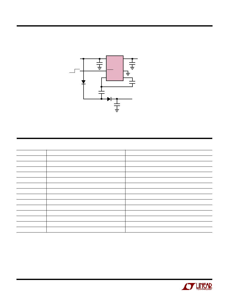
Ultralow Quiescent Current Regulated Supply
The LTC1983 contains an internal resistor divider (refer to
the Block Diagram) that draws only 1
µ
A (typ for the 3V
version) from V
OUT
during normal operation. During shut-
down, the resistor divider is disconnected from the output
and the part draws only leakage current from the output.
During no-load conditions, applying a 1Hz to 100Hz, 2%
to 5% duty cycle signal to the SHDN pin ensures that the
circuit of Figure 2 comes out of shutdown frequently
enough to maintain regulation even under low-load condi-
tions. Since the part spends nearly all of its time in
shutdown, the no-load quiescent current is essentially
zero. However, the part will still be in operation during the
time the SHDN pin is high, so the current will not be zero
and can be calculated using the following equations to
determine the approximate maximum current: I
IN(MAX)
=
[(Time out of shutdown) ∑ (Burst Mode operation quies-
cent current) + (Normal operating I
IN
) ∑ (Time output is
being charged before the LTC1983 enters Burst Mode
operation)]/(Period of SHDN signal). This number will be
highly dependent on the amount of board leakage current
and how many devices are connected to V
OUT
(each will
draw some leakage current) and must be calculated and
verified for each different board design.
The LTC1983 must be out of shutdown for a minimum
duration of 200
µ
s to allow enough time to sense the output
and keep it in regulation. A 1Hz, 2% duty cycle signal will
keep V
OUT
in regulation under no-load conditions. Even
though the term no-load is used, there will always be board
leakage current and leakage current drawn by anything
connected to V
OUT
. This is why it is necessary to wake the
part up every once in a while to verify regulation. As the
V
OUT
load current increases, the frequency with which the
part is taken out of shutdown must also be increased to
prevent V
OUT
from drooping below the ≠ 2.88V (for the 3V
version) during the OFF phase (see Figure 3). A 100Hz, 2%
duty cycle signal on the SHDN pin ensures proper regula-
tion with load currents as high as 100
µ
A. When load
current greater than 100
µ
A is needed, the SHDN pin must
be forced high as in normal operation.
Each time the LTC1983 comes out of shutdown, the part
delivers a minimum of one clock cycle worth of charge to
the output. Under high V
IN
(>4V) and/or low I
OUT
(<10
µ
A)
conditions, this behavior may cause a net excess of charge
to be delivered to the output capacitor if a high frequency
signal is used on the SHDN pin (e.g., 50Hz to 100Hz).
Under such conditions, V
OUT
will slowly drift positive and
may even go out of regulation. To avoid this potential
Figure 2. Ultralow Quiescent Current Regulated Supply
V
IN
GND
C
+
SHDN
V
OUT
C
≠
LTC1983-3
C
FLY
1
µ
F
CERAMIC
FROM MPU
SHDN
V
IN
C
IN
10
µ
F
TANTALUM
C
OUT
10
µ
F
CERAMIC
SHDN PIN WAVEFORMS:
LOW I
Q
MODE
(I
OUT
100
µ
A)
V
OUT
LOAD ENABLE MODE
(I
OUT
= 100
µ
A TO 100mA)
(1Hz TO 100Hz, 2% TO 5% DUTY CYCLE)
≠3V
±
4%
1983 F02
3.3V TO 5.5V
OPERATIO
U
(Refer to Block Diagram)
LTC1983-3/LTC1983-5
9
sn1983 1983fs
problem in the low I
Q
mode, it is necessary to switch the
part in and out of shutdown at the minimum allowable
frequency (refer to Figure 3) for a given output load.
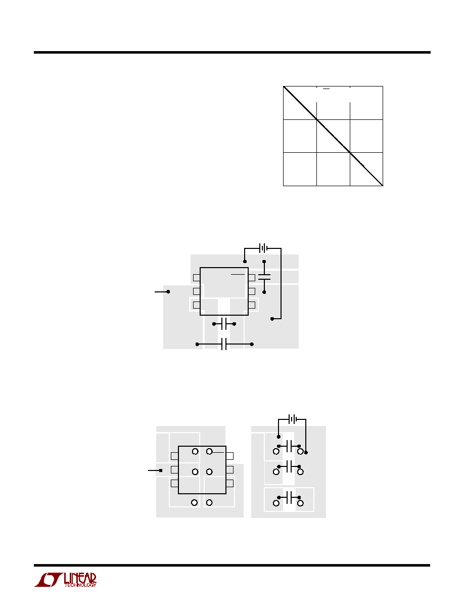
General Layout Considerations
Due to the high switching frequency and high transient
currents produced by the LTC1983, careful board layout is
a must. A clean board layout using a ground plane and
short connections to all capacitors will improve perfor-
mance and ensure proper regulation under all conditions
(refer to Figures 4a and 4b). You will not get advertised
performance with careless layout.
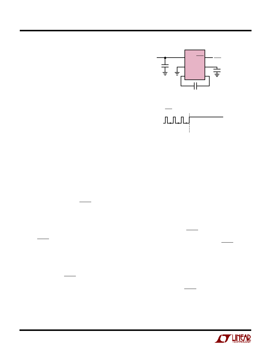
Figure 3
OUTPUT CURRENT (
µ
A)
1
10
100
1000
MAXIMUM SHDN OFF TIME (ms)
1000
1983 F03b
1
10
100
SHDN ON PULSE WIDTH = 200
µ
s
C
OUT
= 10
µ
F
Figure 4a. Recommended Component
Placement for a Single Layer Board
Figure 4b. Recommended Component
Placement for a Double Layer Board
1 V
IN
2 V
OUT
3 C
+
SHDN 6
GND 5
C
≠
4
C
OUT
C
FLY
V
IN
: 2.3V TO 5.5V
V
OUT
1983 F04a
C
IN
1 V
IN
2 V
OUT
3 C
+
SHDN 6
GND 5
C
≠
4
C
IN
C
OUT
C
FLY
V
OUT
1983 F04b
BOTTOM LAYER
TOP LAYER
OPERATIO
U
(Refer to Block Diagram)
LTC1983-3/LTC1983-5
10
sn1983 1983fs
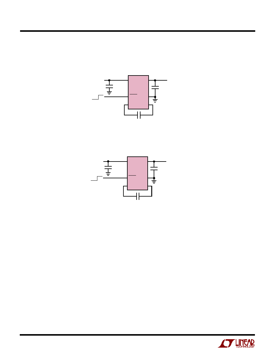
TYPICAL APPLICATIO S
U
V
IN
SHDN
C
+
V
OUT
GND
C
≠
LTC1983-5
V
IN
2.5V TO 5.5V
V
OUT
≠V
IN
10
µ
F
10
µ
F
CERAMIC
1
µ
F
CERAMIC
OFF ON
1983 TA04
V
IN
SHDN
C
+
V
OUT
GND
C
≠
LTC1983-5
V
IN
2.5V
V
OUT
≠2.5V
1
µ
F
CERAMIC
4.7
µ
F
CERAMIC
0.47
µ
F
CERAMIC
OFF ON
1983 TA03
2.5V to ≠2.5V DC/DC Converter
100mA Inverting DC/DC Converter

LTC1983-3/LTC1983-5
11
sn1983 1983fs
PACKAGE DESCRIPTIO
U
Information furnished by Linear Technology Corporation is believed to be accurate and reliable.
However, no responsibility is assumed for its use. Linear Technology Corporation makes no represen-
tation that the interconnection of its circuits as described herein will not infringe on existing patent rights.
S6 Package
6-Lead Plastic SOT-23
(Reference LTC DWG # 05-08-1636)
1.50 ≠ 1.75
(NOTE 4)
2.80 BSC
0.30 ≠ 0.45 TYP
6 PLCS (NOTE 3)
DATUM `A'
0.09 ≠ 0.20
(NOTE 3)
S6 TSOT-23 0801
2.90 BSC
(NOTE 4)
0.95 BSC
1.90 BSC
0.80 ≠ 0.90
1.00 MAX
0.01 ≠ 0.10
0.20 BSC
0.30 ≠ 0.50 REF
PIN ONE ID
NOTE:
1. DIMENSIONS ARE IN MILLIMETERS
2. DRAWING NOT TO SCALE
3. DIMENSIONS ARE INCLUSIVE OF PLATING
4. DIMENSIONS ARE EXCLUSIVE OF MOLD FLASH AND METAL BURR
5. MOLD FLASH SHALL NOT EXCEED 0.254mm
6. JEDEC PACKAGE REFERENCE IS MO-193
3.254
0.754
0.95 BSC
0.854
±
0.127
RECOMMENDED SOLDER PAD LAYOUT
1.9 BSC
LTC1983-3/LTC1983-5
12
sn1983 1983fs
Linear Technology Corporation
1630 McCarthy Blvd., Milpitas, CA 95035-7417
(408) 432-1900
q
FAX: (408) 434-0507
q
www.linear.com
©
LINEAR TECHNOLOGY CORPORATION 2002
LT/TP 0302 2K ∑ PRINTED IN USA
RELATED PARTS
PART NUMBER
DESCRIPTION
COMMENTS
LTC1261
Switched-Capacitor Regulated Voltage Inverter
Selectable Fixed Output Voltages
LTC1261L
Switched-Capacitor Regulated Voltage Inverter
Adjustable and Fixed Output Voltages, Up to 20mA I
OUT
, MSOP
LTC1429
Clock-Synchronized Switched-Capacitor Voltage Inverter
Synchronizable Up to 2MHz System Clock
LTC1514/LTC1515
Step-Up/Step-Down Switched-Capacitor DC/DC Converters
V
IN
2V to 10V, Adjustable or Fixed V
OUT
, I
OUT
to 50mA
LTC1516
Micropower Regulated 5V Charge Pump DC/DC Converter
I
OUT
= 20mA (V
IN
2V), I
OUT
= 50mA (V
IN
3V)
LTC1522
Micropower Regulated 5V Charge Pump DC/DC Converter
I
OUT
= 10mA (V
IN
2.7V), I
OUT
= 20mA (V
IN
3V)
LTC1550L/LTC1551L
Low Noise, Switched-Capacitor Regulated Voltage Inverters 900kHz Charge Pump, 1mV
P-P
Ripple
LT1611
1.4MHz Inverting Mode Switching Regulator
≠5V at 150mA from a 5V Input, 5-Lead ThinSOT
LT1617/LT1617-1
Micropower, Switched-Capacitor Voltage Inverter
V
IN
1.2V/1V to 15V; 350mA/100mA Current Limit
LTC1682/-3.3/-5
Doubler Charge Pumps with Low Noise LDO
MS8 and SO-8 Packages, I
OUT
= 80mA, Output Noise = 60
µ
V
RMS
LTC1751/-3.3/-5
Doubler Charge Pumps
V
OUT
=5V at 100mA; V
OUT
=3.3V at 80mA; ADJ; MSOP Packages
LTC1754/-3.3/-5
Doubler Charge Pumps with Shutdown
ThinSOT Package; I
Q
= 13
µ
A; I
OUT
= 50mA
LTC1928-5
Doubler Charge Pump with Low Noise LDO
ThinSOT Output Noise = 60
µ
V
RMS
; V
OUT
= 5V; V
IN
= 2.7V to 4V
LTC3200
Constant Frequency Doubler Charge Pump
Low Noise, 5V Output or Adjustable
Combined Unregulated Doubler
and Regulated Inverter
U
TYPICAL APPLICATIO
C
+
C
≠
LTC1983-3/
LTC1983-5
C
FLY
1
µ
F
CERAMIC
C
BOOST
1
µ
F
OFF ON
C
OUT2
10
µ
F
CERAMIC
C
OUT1
10
µ
F
CERAMIC
C
IN
10
µ
F
CERAMIC
1983 TA05
V
IN
V
IN
V
OUT
V
OUT
SHDN
GND
D1
D2
V
BOOST
V
BOOST
= 2V
IN
≠2(V
D
)