1
LTC1986
s
V
IN
Range: 2.6V to 4.4V
s
Step-Up Charge Pump Generates 5V
s
Output Current: 10mA
s
V
IN
to V
OUT
Direct Connection for 3V SIMs
s
Ultralow Power
Operating Current: 14
µ
A
Shutdown Current: <1
µ
A
s
No Inductors
s
Short-Circuit/Thermal Protected
s
Switching Frequency: 900kHz
s
Soft-Start Limits Inrush Current at Turn-On
s
Output Driven to Ground During Shutdown
s
Ultrasmall Application Circuit (< 0.045in
2
)
s
6-Lead SOT-23 Package
The LTC
Æ
1986 is a micropower charge pump DC/DC
converter that provides power for either 3V or 5V GSM
SIM cards. It operates in one of three modes: V
OUT
= 5V
(5V mode), V
OUT
= V
IN
(3V mode) or shutdown. The input
voltage range is 2.6V to 4.4V and the part can provide
10mA of output current. The LTC1986 allows V
IN
to drop
as low as 2.6V by providing a boost feature in 3V mode. In
3V mode, V
OUT
is connected directly to V
IN
through a 2.5
switch until V
IN
drops below 2.85V. When V
IN
is below
2.85V, the part automatically boosts V
OUT
to maintain a
regulated 2.9V output, thereby ensuring V
OUT
stays within
the 3V SIM V
CC
specification.
Extremely low operating current (14
µ
A typical with no
load) and low external parts count make the part ideally
suited for small, light load battery-powered applications.
The total PCB area of the application circuit shown below
is less than 0.045in
2
. Protection features include inrush
current limiting, undervoltage lockout, short circuit and
thermal overload protection. The LTC1986 is available in
a 6-lead SOT-23 package.
s
GSM Cellular Telephones
s
PCS/DCS Cellular Telephones
s
Portable POS Terminals
3V/5V SIM Power Supply
in SOT-23
, LTC and LT are registered trademarks of Linear Technology Corporation.
V
OUT
GND
MODE
V
IN
C1
+
C1
≠
1
2
3
6
5
4
V
OUT
= 5V
OR V
IN
GSM
CONTROLLER
2.2
µ
F
0.047
µ
F
0.1
µ
F
V
IN
= 2.6V TO 4.4V
LTC1986
750k
1M
3/5
SHDN
1986 TA01
SHDN
0
0
1
1
3/5
0
1
0
1
MODE
SHUTDOWN
SHUTDOWN
V
OUT
= 5V
V
OUT
= V
IN
3V/5V SIM Power Supply
INPUT VOLTAGE (V)
2.5
OUTPUT VOLTAGE (V)
4
5
4.5
1986 TA02
3
2
3.0
3.5
4.0
6
T
A
= 25
∞
C
I
OUT
= 10mA
5V MODE
3V MODE
(V
OUT
= V
IN
)
Output Voltage vs Input Voltage
APPLICATIO S
U
FEATURES
TYPICAL APPLICATIO
U
DESCRIPTIO
U
2
LTC1986
Note 1: Absolute Maximum Ratings are those values beyond which the life
of a device may be impaired.
PARAMETER
CONDITIONS
MIN
TYP
MAX
UNITS
V
IN
Operating Voltage
q
2.6
4.4
V
V
OUT
Output Voltage
Shutdown Mode
0
V
3V Mode. V
IN
= 2.85V to 4.4V, I
OUT
10mA
V
IN
≠ 0.025
V
3V Mode, V
IN
< 2.85V, I
OUT
< 10mA
q
2.75
2.9
3.05
V
5V Mode, V
IN
< 2.7V, I
OUT
10mA
q
4.55
5
5.25
V
5V Mode, V
IN
= 2.7V to 4.4V, I
OUT
10mA
q
4.75
5
5.25
V
V
IN
Operating Current
Shutdown Mode, V
MODE
= 0V
q
0.001
1
µ
A
3V Mode, I
OUT
= 0mA
q
10
25
µ
A
5V Mode, I
OUT
= 0mA
q
14
30
µ
A
V
IN
-to-V
OUT
ON Resistance
3V Mode, V
IN
= 3V
q
2.5
5
V
OUT
Short-Circuit Current
3V or 5V Mode, V
OUT
= 0V
q
20
100
200
mA
V
OUT
Discharge Resistance
q
70
200
Switching Frequency
Oscillator Free-Running
900
kHz
MODE Input Ranges
Shutdown Mode
q
0
V
IN
/2 ≠ 0.1
V
5V Mode
q
V
IN
/2 + 0.1
V
IN
≠ 1.0
V
3V Mode
q
V
IN
≠ 0.25
V
IN
V
MODE Input Current
q
≠1
1
µ
A
Undervoltage Lockout Threshold
1.4
V
LTC1986ES6
T
JMAX
= 125
∞
C,
JA
= 230
∞
C/ W
ORDER PART
NUMBER
V
IN
, V
OUT
to GND .........................................≠ 0.3V to 6V
All Other Pins to GND .................................. ≠ 0.3V to 6V
V
OUT
Short-Circuit Duration ............................. Indefinite
Operating Temperature Range
(Note 2) .................................................. ≠ 40
∞
C to 85
∞
C
Storage Temperature Range ................. ≠ 65
∞
C to 150
∞
C
Lead Temperature (Soldering, 10 sec).................. 300
∞
C
(Note 1)
ABSOLUTE
M
AXI
M
U
M
RATINGS
W
W
W
U
PACKAGE/ORDER I
N
FOR
M
ATIO
N
W
U
U
ELECTRICAL CHARACTERISTICS
Consult factory for Military grade parts.
The
q
denotes specifications which apply over the full operating temperature range, otherwise specifications are T
A
= 25
∞
C.
V
IN
= V
MIN
to V
MAX
, MODE = V
IN
, C1 = 0.047
µ
F, C
OUT
= 2.2
µ
F, unless otherwise specified.
V
OUT
1
GND 2
MODE 3
TOP VIEW
S6 PACKAGE
6-LEAD PLASTIC SOT-23
6 V
IN
5 C1
+
4 C1
≠
Note 2: The LTC1986 is guaranteed to meet performance specifications
from 0
∞
C to 70
∞
C. Specifications over the ≠ 40
∞
C to 85
∞
C operating
temperature range are assured by design, characterization and correlation
with statistical process controls.
S6 PART MARKING
LTKX
3
LTC1986
TYPICAL PERFOR
M
A
N
CE CHARACTERISTICS
U
W
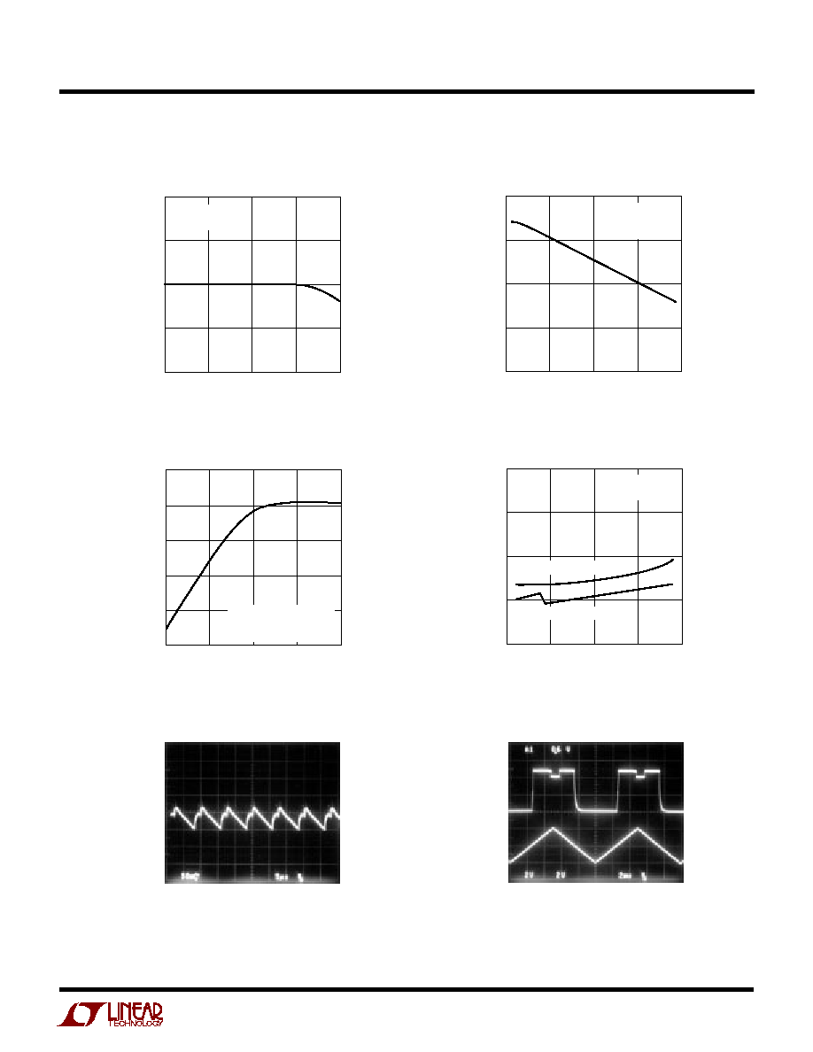
Output Voltage vs Output Current
(3V Mode)
OUTPUT CURRENT (mA)
0.001
OUTPUT VOLTAGE (V)
10
1986 G01
0.01
0.1
1
3.10
3.05
3.00
2.95
2.90
V
IN
= V
MODE
= 3V
T
A
= 25
∞
C
INPUT VOLTAGE (V)
2.5
EFFICIENCY (%)
4.5
1986 G02
3.0
3.5
4.0
100
80
60
40
20
I
OUT
= 10mA
V
OUT
= 5V
T
A
= 25
∞
C
Efficiency vs Input Voltage
Efficiency vs Output Current
Positive Supply Current vs
Input Voltage
OUTPUT CURRENT (mA)
0.001
EFFICIENCY (%)
10
1986 G03
0.01
0.1
1
100
80
60
40
20
0
V
IN
= 3V
5V MODE (V
MODE
= 0.6V
IN
)
T
A
= 25
∞
C
INPUT VOLTAGE (V)
2.5
POSITIVE SUPPLY CURRENT (mA )
4.5
1986 G04
3.0
3.5
4.0
40
30
20
10
0
I
OUT
= 0mA
T
A
= 25
∞
C
5V MODE (V
MODE
= 0.6V
IN
)
3V MODE (V
MODE
= V
IN
)
Output Voltage Ripple
(5V Mode)
V
OUT
50mV/DIV
AC COUPLED
Output Voltage vs
V
MODE
Waveforms
5ms/DIV
V
IN
= 3V
I
OUT
= 10mA
T
A
= 25
∞
C
1986 G05
V
OUT
2V/DIV
2ms/DIV
V
IN
= 4V
T
A
= 25
∞
C
1986 G06
5V
0V
4V
0V
V
MODE
2V/DIV
4
LTC1986
V
OUT
(Pin 1): Charge Pump Output. The V
OUT
voltage will
depend on the MODE pin input voltage. V
OUT
= 0V in
shutdown mode, V
OUT
= V
IN
in 3V mode and V
OUT
= 5V in
5V mode. The LTC1986 provides a 2.9V regulated output
when the part is in 3V mode and the V
IN
voltage is below
2.85V. This feature allows the input voltage to be below the
minimum voltage specification for 3V SIM cards without
violating the SIM V
CC
specification. Bypass the V
OUT
pin
with a
2.2
µ
F low ESR capacitor to ground.
GND (Pin 2): Ground. Connect to a ground plane for best
performance.
MODE (Pin 3): MODE Input Pin. The voltage on this pin
determines the operating mode of the LTC1986. It oper-
ates in either shutdown mode, 3V mode or 5V mode
depending on the MODE pin voltage with respect to V
IN
.
PI
N
FU
N
CTIO
N
S
U
U
U
The three different modes can be realized by using two
external resistors as shown in the typical application
circuit. If V
MODE
< V
IN
/2 ≠ 0.1V, the part is in shutdown
mode.If V
IN
/2 + 0.1V < V
MODE
< V
IN
≠ 1V, the part is in 5V
mode. If V
IN
≠ 0.25V < V
MODE
, the part is in 3V mode. To
achieve the lowest possible shutdown current, the MODE
pin should be pulled to 0V, i.e., both the SHDN and 3/5
signals from the controller should be pulled low.
C1
≠
(Pin 4): Charge Pump Flying Capacitor Negative
Terminal.
C1
+
(Pin 5): Charge Pump Flying Capacitor Positive
Terminal.
V
IN
(Pin 6): Input Supply Voltage. Bypass V
IN
with a
0.1
µ
F low ESR capacitor to ground.
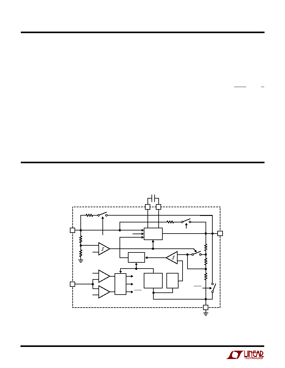
SI PLIFIED
W
BLOCK DIAGRA
W
3V
5V
SHDN
+
≠
+
≠
+
≠
MODE
6
3
V
IN
V
OUT
V
IN
≠ 0.6V
V
IN
/2
1.25V
LOGIC
UVLO/
THERMAL
SHDN
CHARGE
PUMP
900kHz
OSC
2.9V BOOST
3V MODE
SOFT START
50
5V MODE
C1
≠
C1
+
1.25V
REF
+
≠
SHDN
GND
1986 BD
LTC1986
2.5
4
5
1
2
5
LTC1986
APPLICATIO
N
S I
N
FOR
M
ATIO
N
W
U
U
U
Operation
The LTC1986 is a charge pump DC/DC converter designed
specifically to supply V
CC
power for either 3V or 5V SIM
cards. The part can operate in one of three modes: a low
power shutdown mode which disconnects V
IN
from V
OUT
and actively pulls down the V
OUT
supply, 3V mode which
provides a direct connection between V
IN
and V
OUT
for
powering 3V SIM cards, and 5V mode which provides a
regulated 5V output for powering 5V SIM cards. In 5V
mode, regulation is achieved by sensing the output volt-
age through a resistor divider and enabling the charge
pump as needed to maintain regulation.
When the charge pump is enabled, a 2-phase
nonoverlapping clock controls the internal charge pump
switches. Flying capacitor C1 is charged to V
IN
on phase
one of the clock. On phase two of the clock, C1 is stacked
in series with V
IN
and connected to V
OUT
through an
internal switch. This sequence of charging and discharg-
ing the flying capacitor occurs at a free-running frequency
of 900kHz (typ) and continues until the divided output
voltage reaches the upper trip point of the comparator.
Once the output is in regulation, the charge pump is
disabled. This method of bursting the charge pump on and
off enables the LTC1986 to achieve high efficiency at
extremely low output loads.
Mode Selection
The operating mode is determined by the voltage applied
to the MODE pin. The MODE pin has three voltage thresh-
olds--all of which are referenced to V
IN
:
Shutdown Mode
V
MODE
< V
IN
/2 ≠ 0.1V
5V Mode
V
IN
/2 + 0.1V < V
MODE
< V
IN
≠ 1V
3V Mode
V
IN
≠ 0.25V < V
MODE
For example, if V
IN
= 3V, then the following table applies:
V
MODE
OPERATING MODE
0V to 1.4V
Shutdown Mode
1.6V to 2V
5V Mode
2.75V to 3V
3V Mode (V
OUT
= V
IN
)
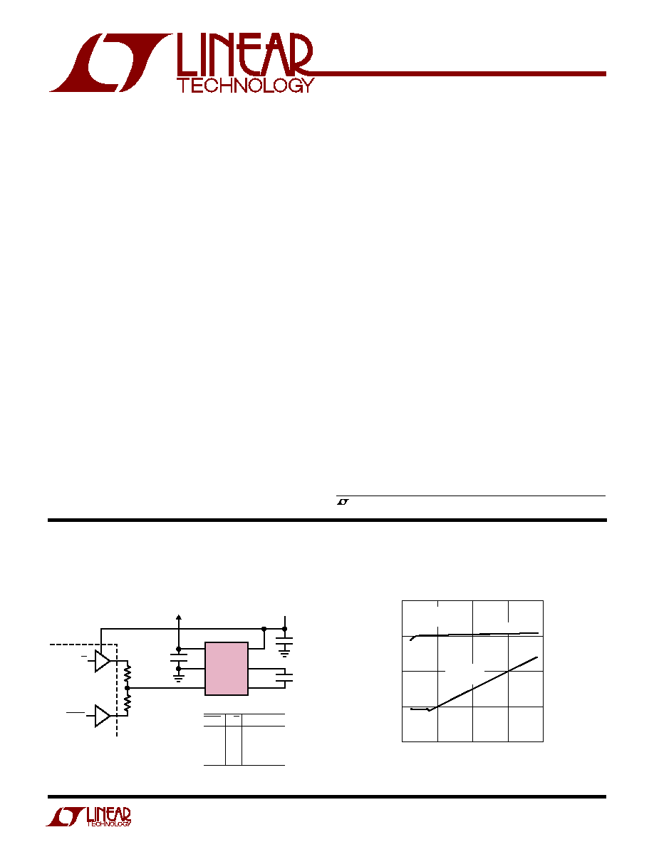
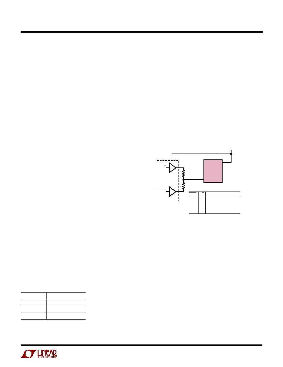
The three modes can be selected using two totem pole
digital outputs and two external resistors as shown in
Figure 1.
Shutdown mode disconnects V
IN
from V
OUT
and enables
an internal pull-down device which forces V
OUT
to GND.
To achieve the lowest possible quiescent current in shut-
down mode, the voltage on the MODE pin should be pulled
below 0.4V. 3V mode connects V
OUT
to V
IN
through a 2.5
internal switch. The LTC1986 has the additional capability
of boosting V
OUT
to a regulated 2.9V in 3V mode when the
input voltage drops below 2.85V. This ensures that the 3V
SIM V
CC
specification is not violated if V
IN
drops below
2.7V during transients or low battery conditions.
Figure 1
Capacitor Selection
For best performance, it is recommended that low ESR
capacitors be used for both C
IN
and C
OUT
to reduce noise
and ripple. The C
IN
and C
OUT
capacitors should be either
ceramic or tantalum. Ceramic capacitors will provide the
smallest size for a given capacitance. If the input source
impedance is very low (< 0.5
), C
IN
may not be needed.
For best performance, C
OUT
should be 2.2
µ
F or greater.
Ceramic capacitors are also recommended for the flying
capacitor C1 with values between 0.047
µ
F and 0.22
µ
F. If
a small value output capacitor (3.3
µ
F or less) is used, a
small flying capacitor should also be used to prevent high
output ripple in 5V mode. The recommended capacitor
values to minimize board space and cost are: C
IN
= 0.1
µ
F,
C1 = 0.047
µ
F and C
OUT
= 2.2
µ
F (ceramic).
MODE
V
IN
3
6
V
IN
LTC1986
750k
1M
3/5
SHDN
1986 F01
SHDN
0
0
1
1
3/5
0
1
0
1
MODE
SHUTDOWN (I
CC
< 1
µ
A)
SHUTDOWN (I
CC
= 10
µ
A)
V
OUT
= 5V
V
OUT
= V
IN