LTC1992
1
1992i
Information furnished by Linear Technology Corporation is believed to be accurate and reliable.
However, no responsibility is assumed for its use. Linear Technology Corporation makes no represen-
tation that the interconnection of its circuits as described herein will not infringe on existing patent rights.
Final Electrical Specifications
s
Differential Driver/Receiver
s
Differential Amplification
s
Single-Ended to Differential Conversion
s
Level Shifting
s
Trimmed Phase Response for Multichannel Systems
s
Fully Differential Input and Output
s
C
LOAD
Stable up to 10,000pF
s
Adjustable Output Common Mode Voltage
s
Rail-to-Rail Output Swing
s
Low Supply Current: 1.2mA (Max)
s
High Output Current: 10mA (Min)
s
Specified on a Single 2.7V to
±
5V Supply
s
DC Offset Voltage <2.5mV (Max)
s
MSOP 8-Lead Package
APPLICATIO S
U
FEATURES
DESCRIPTIO
U
TYPICAL APPLICATIO
U
Fully Differential
Input/Output Amplifier/Driver
July 2003
, LTC and LT are registered trademarks of Linear Technology Corporation.
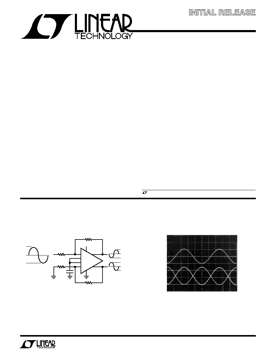
Single-Ended to Differential Conversion
The LTC
Æ
1992 is a fully differential low power amplifier.
The LTC1992 has a separate internal common mode
feedback path for outstanding output phase balancing and
reduced second order harmonics. The V
OCM
pin sets the
output common mode level independent of the input
common mode level. This feature makes level shifting of
signals easy.
The differential inputs operate with signals ranging from
rail-to-rail with a common mode level from the negative
supply up to 1.3V from the positive supply. The differential
input DC offset is typically 250
µ
V. The rail-to-rail outputs
sink and source 10mA. The LTC1992 is stable for all
capacitive loads up to 10,000pF.
The LTC1992 can be used in single-supply applications
with supply voltages as low as 2.7V. It can also be used
with dual supplies up to
±
5V. The LTC1992 is available in
an 8 pin MSOP package.
≠
≠
+
+
5V
5V
LTC1992
3
6
V
OCM
V
MID
0V
2.5V
0V
V
IN
0.01
µ
F
1992 TA01a
4
5
2
7
8
1
10k
10k
10k
10k
5V
0V
5V
≠5V
2.5V
INPUT SIGNAL
FROM A
±
5V SYSTEM
OUTPUT SIGNAL
FROM A
SINGLE-SUPPLY SYSTEM
V
IN
(5V/DIV)
+OUT
≠OUT
(2V/DIV)
5V
0V
≠5V
5V
0V
1992 TA01b
LTC1992
2
1992i
LTC1992CMS8
LTC1992ISM8
LTC1992HMS8
SYMBOL
PARAMETER
CONDITIONS
MIN
TYP
MAX
MIN
TYP
MAX
UNITS
V
OSDIFF
Differential Offset Voltage
V
S
= 2.7V
q
±
0.25
±
2.5
±
0.25
±
4
mV
(Input Referred)
V
S
= 5V
q
±
0.25
±
2.5
±
0.25
±
4
mV
V
S
=
±
5V
q
±
0.25
±
2.5
±
0.25
±
4
mV
V
OSDIFF
/
T
Differential Offset Voltage Drift
V
S
= 2.7V
q
10
10
µ
V/
∞
C
(Input Referred)
V
S
= 5V
q
10
10
µ
V/
∞
C
V
S
=
±
5V
q
10
10
µ
V/
∞
C
I
B
Input Bias Current
V
S
= 2.7V to
±
5V
q
2
250
2
400
pA
I
OS
Input Offset Current
V
S
= 2.7V to
±
5V
q
0.1
100
0.1
150
pA
R
IN
Input Resistance
q
500
500
M
C
IN
Input Capacitance
q
3
3
pF
e
n
Input Referred Noise Voltage Density f = 10Hz
100
100
nV/
Hz
f = 1kHz
18
18
nV/
Hz
i
n
Input Noise Current Density
f = 10Hz
1
1
pA/
Hz
f = 1kHz
1
1
pA/
Hz
V
INCMR
Input Signal Common Mode Range
q
V
CMRR
Common Mode Rejection Ratio
V
INCM
= ≠0.1V to 3.7V
q
69
90
69
90
dB
(Input Referred)
PSRR
Power Supply Rejection Ratio
V
S
= 2.7V to
±
5V
q
75
80
72
80
dB
(Input Referred)
G
CM
Common Mode Gain(V
OUTCM
/V
OCM
)
q
1
1
Common Mode Gain Error
q
±
0.1
±
0.3
±
0.1
±
0.35
%
Output Balance (
V
OUTCM
/(V
OUTDIFF
) V
OUTDIFF
= ≠2V to +2V
q
≠85
≠60
≠85
≠60
dB
V
OSCM
Common Mode Offset Voltage
V
S
= 2.7V
q
±
0.5
±
12
±
0.5
±
15
mV
(V
OUTCM
≠ V
OCM
)
V
S
= 5V
q
±
1
±
15
±
1
±
17
mV
V
S
=
±
5V
q
±
2
±
18
±
2
±
20
mV
V
OSCM
/
T
Common Mode Offset Voltage Drift
V
S
= 2.7V
q
10
10
µ
V/
∞
C
V
S
= 5V
q
10
10
µ
V/
∞
C
V
S
=
±
5V
q
10
10
µ
V/
∞
C
Total Supply Voltage (+V
S
to ≠V
S
) .......................... 12V
Maximum Voltage
on any Pin .......... (≠V
S
≠ 0.3V)
V
PIN
(+V
S
+ 0.3V)
Output Short-Circuit Duration (Note 3) ............ Indefinite
Operating Temperature Range (Note 5)
LTC1992CMS8/LTC1992IMS8 ............≠40
∞
C to 85
∞
C
LTC1992HMS8 ..................................≠40
∞
C to 125
∞
C
Specified Temperature Range (Note 6)
LTC1992CMS8/LTC1992IMS8 ............≠40
∞
C to 85
∞
C
LTC1992HMS8 ..................................≠40
∞
C to 125
∞
C
Storage Temperature Range ................ ≠ 65
∞
C to 150
∞
C
Lead Temperature (Soldering, 10 sec).................. 300
∞
C
ORDER PART
NUMBER
T
JMAX
= 150
∞
C,
JA
= 250
∞
C/W
LTC1992CMS8
LTC1992IMS8
LTC1992HMS8
ABSOLUTE AXI U
RATI GS
W
W
W
U
PACKAGE/ORDER I FOR ATIO
U
U
W
(Note 1)
ELECTRICAL CHARACTERISTICS
The
q
denotes specifications which apply over the full operating
temperature range, otherwise specifications are at T
A
= 25
∞
C. +V
S
= 5V, ≠V
S
= 0V, V
INCM
= V
OUTCM
= V
OCM
= 2.5V, unless otherwise
noted. V
OCM
is the voltage on the V
OCM
pin. V
OUTCM
is defined as (V
+OUT
+ V
≠ OUT
)/2. V
INCM
is defined as (V
+IN
+ V
≠IN
)/2. V
INDIFF
is
defined as (V
+IN
≠ V
≠ IN
). V
OUTDIFF
is defined as (V
+OUT
≠ V
≠OUT
).
Consult LTC Marketing for parts specified with wider operating temperature ranges.
1
2
3
4
≠IN
V
OCM
+V
S
+OUT
8
7
6
5
+IN
V
MID
≠V
S
≠OUT
TOP VIEW
MS8 PACKAGE
8-LEAD PLASTIC MSOP
+
+
≠
≠
MS8 PART MARKING
LTYU
LTZC
LTAGR
(≠V
S
)≠ 0.1V (+V
S
)≠ 1.3V
(≠V
S
)≠ 0.1V (+V
S
)≠ 1.3V
LTC1992
3
1992i
LTC1992CMS8
LTC1992ISM8
LTC1992HMS8
SYMBOL
PARAMETER
CONDITIONS
MIN
TYP
MAX
MIN
TYP
MAX
UNITS
V
OUTCMR
Output Signal Common Mode Range
q
V
(Voltage Range for the V
OCM
Pin)
R
INVOCM
Input Resistance, V
OCM
Pin
q
500
500
M
I
BVOCM
Input Bias Current, V
OCM
Pin
V
S
= 2.7V to
±
5V
q
±
2
2
pA
V
MID
Voltage at the V
MID
Pin
q
2.44
2.50
2.56
2.43
2.50
2.57
V
V
OUT
Output Voltage, High
V
S
= 2.7V, Load = 10k
q
2.60
2.69
2.60
2.69
V
(Note 2)
V
S
= 2.7V, Load = 5mA
q
2.50
2.61
2.50
2.61
V
V
S
= 2.7V,Load = 10mA
q
2.29
2.52
2.29
2.52
V
Output Voltage, Low
V
S
= 2.7V, Load = 10k
q
0.02
0.10
0.02
0.10
V
(Note 2)
V
S
= 2.7V, Load = 5mA
q
0.10
0.25
0.10
0.25
V
V
S
= 2.7V, Load = 10mA
q
0.20
0.35
0.20
0.41
V
Output Voltage, High
V
S
= 5V, Load = 10k
q
4.90
4.99
4.90
4.99
V
(Note 2)
V
S
= 5V, Load = 5mA
q
4.85
4.90
4.80
4.90
V
V
S
= 5V, Load = 10mA
q
4.75
4.81
4.70
4.81
V
Output Voltage, Low
V
S
= 5V, Load = 10k
q
0.02
0.10
0.02
0.10
V
(Note 2)
V
S
= 5V, Load = 5mA
q
0.10
0.25
0.10
0.30
V
V
S
= 5V, Load = 10mA
q
0.20
0.35
0.20
0.42
V
Output Voltage, High
V
S
=
±
5V, Load = 10k
q
4.90
4.99
4.85
4.99
V
(Note 2)
V
S
=
±
5V, Load = 5mA
q
4.85
4.89
4.80
4.89
V
V
S
=
±
5V, Load = 10mA
q
4.65
4.80
4.60
4.80
V
Output Voltage, Low
V
S
=
±
5V, Load = 10k
q
≠ 4.99
≠4.90
≠4.98
≠4.85
V
(Note 2)
V
S
=
±
5V, Load = 5mA
q
≠ 4.90
≠4.75
≠4.90
≠4.75
V
V
S
=
±
5V, Load = 10mA
q
≠ 4.80
≠4.65
≠4.80
≠4.55
V
I
SC
Output Short-Circuit Current
V
S
= 2.7V, V
OUT
= 1.35V
q
20
30
20
30
mA
Sourcing (Notes 2,3)
V
S
= 5V, V
OUT
= 2.5V
q
20
30
20
30
mA
V
S
=
±
5V, V
OUT
= 0V
q
20
30
20
30
mA
Output Short-Circuit Current Sinking
V
S
= 2.7V, V
OUT
=1.35V
q
13
30
13
30
mA
(Notes 2,3)
V
S
= 5V, V
OUT
= 2.5V
q
13
30
13
30
mA
V
S
=
±
5V, V
OUT
= 0V
q
13
30
13
30
mA
SR
Slew Rate (Note 4)
q
0.25
0.75
0.25
0.75
V/
µ
s
GBW
Gain-Bandwidth Product
T
A
= 25
∞
C
3.0
3.2
3.5
3.0
3.2
3.5
MHz
(f
TEST
= 100kHz)
LTC1992CMS8
q
2.5
3.0
4.0
MHz
LTC1992IMS8/LTC1992HMS8
q
1.9
4.0
1.9
4.0
MHz
A
VOL
Large-Signal Voltage Gain
q
80
80
dB
V
S
Supply Voltage Range
q
2.7
11
2.7
11
V
I
S
Supply Current
V
S
= 2.7V to 5V
0.65
1.0
0.65
1
mA
q
0.75
1.2
0.8
1.5
mA
V
S
=
±
5V
0.7
1.2
0.7
1.2
mA
q
0.8
1.5
0.9
1.8
mA
The
q
denotes specifications which apply over the full operating
temperature range, otherwise specifications are at T
A
= 25
∞
C. +V
S
= 5V, ≠V
S
= 0V, V
INCM
= V
OUTCM
= V
OCM
= 2.5V, unless otherwise
noted. V
OCM
is the voltage on the V
OCM
pin. V
OUTCM
is defined as (V
+OUT
+ V
≠OUT
)/2. V
INCM
is defined as (V
+IN
+ V
≠IN
)/2. V
INDIFF
is
defined as (V
+IN
≠ V
≠IN
). V
OUTDIFF
is defined as (V
+OUT
≠ V
≠OUT
).
ELECTRICAL CHARACTERISTICS
Note 1: Absolute Maximum Ratings are those values beyond which the life
of a device may be impaired.
Note 2: Output load is connected to the midpoint of the +V
S
and ≠V
S
potentials. Measurement is taken single-ended, one output loaded at a
time.
Note 3: A heat sink may be required to keep the junction temperature
below the absolute maximum when the output is shorted indefinitely.
Note 4: Slew Rate is measured single-ended. The numbers listed are also
single-ended and the differential slew rate would double the listed
numbers.
Note 5: The LTC1992CMS8 and LTC1992IMS8 are guaranteed functional
over an operating temperature of ≠40
∞
C to 85
∞
C. The LTC1992HMS8 is
guaranteed functional over the extended operating temperature of
≠ 40
∞
C to 125
∞
C.
Note 6: The LTC1992CMS8 is guaranteed to meet the specified
performance limits over the 0
∞
C to 70
∞
C temperature range and is
designed, characterized and expected to meet the specified performance
limits over the ≠40
∞
C to 85
∞
C temperature range but is not tested or QA
sampled at these temperatures. The LTC1992IMS8 is guaranteed to meet
the specified performance limits over the ≠40
∞
C to 85
∞
C temperature
range. The LTC1992HMS8 is guaranteed to meet the specified
performance limits over the ≠40
∞
C to 125
∞
C temperature range.
(≠V
S
)+0.5V (+V
S
)≠ 1.3V (≠V
S
)+0.5V (+V
S
)≠ 1.3V

LTC1992
4
1992i
Linear Technology Corporation
1630 McCarthy Blvd., Milpitas, CA 95035-7417
(408) 432-1900
q
FAX: (408) 434-0507
q
www.linear.com
©
LINEAR TECHNOLOGY CORPORATION 2003
LT/TP 0703 1K ∑ PRINTED IN USA
RELATED PARTS
PART NUMBER
DESCRIPTION
COMMENTS
LT1167
Precision Instrumentation Amplifier
Single Resistor Sets the Gain
LTC1992-2
Differential In/Out Amplifier with Gain of 2
Trimmed Phase Response, Rail-to-Rail Output
LT6600-20
Differential In/Out Amplifier and 20MHz Lowpass Filter
Very Low Noise, Standard Differential Amplifier Pinout
≠IN, +IN (Pins 1, 8): Inverting and Noninverting Inputs of
the Amplifier.
V
OCM
(Pin 2): Output Common Mode Voltage Set Pin. The
voltage on this pin sets the output signal's common mode
voltage level. The output common mode level is set
independent of the input common mode level. This is a
high impedance input and must be connected to a known
and controlled voltage. It must never be left floating.
+V
S
, ≠V
S
(Pins 3, 6): The +V
S
and ≠V
S
power supply pins
should be bypassed with 0.1
µ
F capacitors to an adequate
analog ground or ground plane. The bypass capacitors
should be located as closely as possible to the supply pins.
U
U
U
PI FU CTIO S
+OUT, ≠OUT (Pins 4, 5): The Positive and Negative
Outputs of the Amplifier. These rail-to-rail outputs are
designed to drive capacitive loads as high as 10,000pF.
V
MID
(Pin 7): Mid-Supply Reference. This pin is connected
to an on-chip resistive voltage divider to provide a mid-
supply reference. This provides a convenient way to set
the output common mode level at half-supply. If used for
this purpose, Pin 2 will be shorted to Pin 7, Pin 7 should
be bypassed with a 0.1
µ
F capacitor to ground. If this
reference voltage is not used, leave the pin floating.
BLOCK DIAGRA
W
+
≠
1
7
2
6
3
8
5
4
+
≠
200k
200k
V
+
V
≠
30k
30k
≠1
1
1
1
A1
A2
+OUT
≠IN
V
MID
V
OCM
+IN
≠OUT
+V
S
≠V
S