2050fa.pm6
1
LTC2050/LTC2050HV
2050fa
APPLICATIO S
U
DESCRIPTIO
U
FEATURES
TYPICAL APPLICATIO
N
U
Zero-Drift
Operational Amplifiers
in SOT-23
s
Thermocouple Amplifiers
s
Electronic Scales
s
Medical Instrumentation
s
Strain Gauge Amplifiers
s
High Resolution Data Acquisition
s
DC Accurate RC Active Filters
s
Low Side Current Sense
s
Maximum Offset Voltage of 3
µ
V
s
Maximum Offset Voltage Drift of 30nV/
°
C
s
Noise: 1.5
µ
V
P-P
(0.01Hz to 10Hz Typ)
s
Voltage Gain: 140dB (Typ)
s
PSRR: 130dB (Typ)
s
CMRR: 130dB (Typ)
s
Supply Current: 0.8mA (Typ)
s
Supply Operation: 2.7V to 6V (LTC2050)
2.7V to
±
5.5V (LTC2050HV)
s
Extended Common Mode Input Range
s
Output Swings Rail-to-Rail
s
Input Overload Recovery Time: 2ms (Typ)
s
Operating Temperature Range: 40
°
C to 125
°
C
s
SOT-23 Package
The LTC
®
2050 and LTC2050HV are zero-drift operational
amplifiers available in the 5- or 6-lead SOT-23 and SO-8
packages. The LTC2050 operates from a single 2.7V to 6V
supply. The LTC2050HV operates on supplies from 2.7V
to
±
5.5V. The current consumption is 800
µ
A and the
versions in the 6-lead SOT-23 and SO-8 packages offer
power shutdown (active low).
The LTC2050, despite its miniature size, features uncom-
promising DC performance. The typical input offset volt-
age and offset drift are 0.5
µ
V and 10nV/
°
C. The almost
zero DC offset and drift are supported with a power supply
rejection ratio (PSRR) and common mode rejection ratio
(CMRR) of more than 130dB.
The input common mode voltage ranges from the negative
supply up to typically 1V from the positive supply. The
LTC2050 also has an enhanced output stage capable of
driving loads as low as 2k
to both supply rails. The open-
loop gain is typically 140dB. The LTC2050 also features a
1.5
µ
V
P-P
DC to 10Hz noise and a 3MHz gain bandwidth
product.
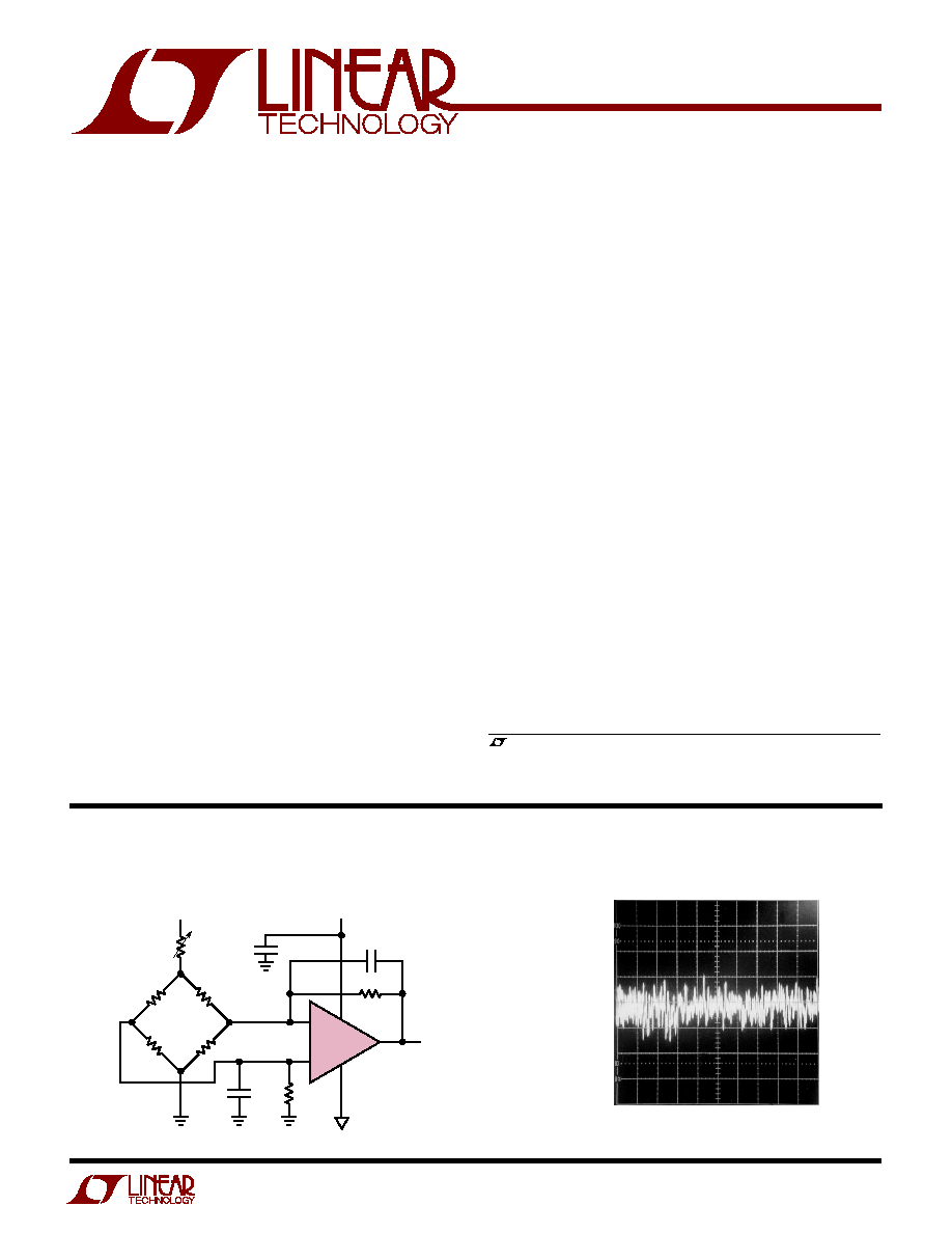
Input Referred Noise 0.1Hz to 10Hz
Differential Bridge Amplifier
, LTC and LT are registered trademarks of Linear Technology Corporation.
+
5V
0.1
µ
F
18.2k
0.1
µ
F
18.2k
5
1
2
3
4
0.1
µ
F
5V
A
V
= 100
2050 TA01
350
STRAIN
GAUGE
50
GAIN
TRIM
LTC2050HV
5V
2
1
0
1
2
µ
V
2
4
0
6
8
10
TIME (SEC)

2
LTC2050/LTC2050HV
2050fa
W
U
U
PACKAGE/ORDER I FOR ATIO
A
U
G
W
A
W
U
W
A
R
BSOLUTE
XI
TI
S
ORDER PART
NUMBER
Total Supply Voltage (V
+
to V
)
LTC2050 .............................................................. 7V
LTC2050HV ......................................................... 12V
Input Voltage ........................ (V
+
+ 0.3V) to (V
0.3V)
Output Short-Circuit Duration ......................... Indefinite
LTC2050CS5
LTC2050IS5
LTC2050HS5
LTC2050HVCS5
LTC2050HVIS5
LTC2050HVHS5
T
JMAX
= 125
°
C,
JA
= 190
°
CW
S5 PART
MARKING
LTAEG
LTAEG
LTAEG
LTAEH
LTAEH
LTAEH
Operating Temperature Range ............. 40
°
C to 125
°
C
Specified Temperature Range
(Note 3) ............................................... 40
°
C to 125
°
C
Storage Temperature Range ................ 65
°
C to 150
°
C
Lead Temperature (Soldering, 10 sec)................. 300
°
C
1
2
3
4
8
7
6
5
TOP VIEW
NC
V
+
OUT
NC
SHDN
IN
+IN
V
S8 PACKAGE
8-LEAD PLASTIC SO
ORDER PART
NUMBER
LTC2050CS6
LTC2050IS6
LTC2050HS6
LTC2050HVCS6
LTC2050HVIS6
LTC2050HVHS6
S6 PART
MARKING
ORDER PART
NUMBER
LTC2050CS8
LTC2050IS8
LTC2050HVCS8
LTC2050HVIS8
S8 PART
MARKING
2050
2050I
2050HV
050HVI
OUT 1
V
2
TOP VIEW
S5 PACKAGE
5-LEAD PLASTIC SOT-23
+IN 3
5 V
+
4 IN
T
JMAX
= 125
°
C,
JA
= 230
°
CW
T
JMAX
= 125
°
C,
JA
= 250
°
CW
OUT 1
V
2
+IN 3
6 V
+
5 SHDN
4 IN
TOP VIEW
S6 PACKAGE
6-LEAD PLASTIC SOT-23
(Note 1)
(LTC2050, LTC2050HV) The
q
denotes specifications which apply over the
full operating temperature range, otherwise specifications are at T
A
= 25
°
C. V
S
= 3V unless otherwise noted. (Note 3)
ELECTRICAL C
C
HARA TERISTICS
LTC2050C/LTC2050I
LTC2050H
PARAMETER
CONDITIONS
MIN
TYP
MAX
MIN
TYP
MAX
UNITS
Input Offset Voltage
(Note 2)
±
0.5
±
3
±
0.5
±
3
µ
V
Average Input Offset Drift
(Note 2)
q
±
0.03
±
0.05
µ
V/
°
C
Long-Term Offset Drift
50
50
nV/
mo
Input Bias Current
LTC2050
±
20
±
75
±
20
±
75
pA
q
±
300
±
4000
pA
LTC2050HV
±
1
±
50
±
1
±
50
pA
q
±
100
±
4000
pA
Input Offset Current
LTC2050
±
150
±
150
pA
q
±
200
±
1000
pA
LTC2050HV
±
100
±
100
pA
q
±
150
±
1000
pA
Input Noise Voltage
R
S
= 100
, 0.01Hz to 10Hz
1.5
1.5
µ
V
P-P
Common Mode Rejection Ratio
V
CM
= GND to (V
+
1.3)
115
130
115
130
dB
V
CM
= GND to (V
+
1.3)
q
110
130
110
130
dB
Consult LTC Marketing for parts specified with wider operating temperature ranges.
LTAEJ
LTAEJ
LTAEJ
LTAEK
LTAEK
LTAEK

3
LTC2050/LTC2050HV
2050fa
LTC2050C/LTC2050I
LTC2050H
PARAMETER
CONDITIONS
MIN
TYP
MAX
MIN
TYP
MAX
UNITS
Power Supply Rejection Ratio
V
S
= 2.7V to 6V
120
130
120
130
dB
q
115
130
115
130
dB
Large-Signal Voltage Gain
R
L
= 10k
120
140
120
140
dB
q
115
140
115
140
dB
Output Voltage Swing High
R
L
= 2k to GND
q
2.85
2.94
2.85
2.94
V
R
L
= 10k to GND
q
2.95
2.98
2.95
2.98
V
Output Voltage Swing Low
R
L
= 2k to GND
q
1
10
1
10
mV
R
L
= 10k to GND
q
1
10
1
10
mV
Slew Rate
2
2
V/
µ
s
Gain Bandwidth Product
3
3
MHz
Supply Current
V
SHDN
= V
IH
, No Load
q
0.75
1.1
0.75
1.2
mA
V
SHDN
= V
IL
q
10
10
µ
A
Shutdown Pin Input Low Voltage (V
IL
)
q
V
+ 0.5
V
+ 0.5
V
Shutdown Pin Input High Voltage (V
IH
)
q
V
+
0.5
V
+
0.5
V
Shutdown Pin Input Current
V
SHDN
= GND
q
0.5
3
0.5
3
µ
A
Internal Sampling Frequency
7.5
7.5
kHz
(LTC2050, LTC2050HV) The
q
denotes specifications which apply over the
full operating temperature range, otherwise specifications are at T
A
= 25
°
C. V
S
= 3V unless otherwise noted. (Note 3)
ELECTRICAL C
C
HARA TERISTICS
LTC2050C/LTC2050I
LTC2050H
PARAMETER
CONDITIONS
MIN
TYP
MAX
MIN
TYP
MAX
UNITS
Input Offset Voltage
(Note 2)
±
0.5
±
3
±
0.5
±
3
µ
V
Average Input Offset Drift
(Note 2)
q
±
0.03
±
0.05
µ
V/
°
C
Long-Term Offset Drift
50
50
nV/
mo
Input Bias Current
LTC2050
±
75
±
150
±
75
±
150
pA
q
±
300
±
4000
pA
LTC2050HV
±
7
±
50
±
7
±
50
pA
q
±
150
±
4000
pA
Input Offset Current
LTC2050
±
300
±
300
pA
q
±
400
±
1000
pA
LTC2050HV
±
100
±
100
pA
q
±
200
±
1000
pA
Input Noise Voltage
R
S
= 100
, 0.01Hz to 10Hz
1.5
1.5
µ
V
P-P
Common Mode Rejection Ratio
V
CM
= GND to (V
+
1.3)
120
130
120
130
dB
V
CM
= GND to (V
+
1.3)
q
115
130
110
130
dB
Power Supply Rejection Ratio
V
S
= 2.7V to 6V
120
130
120
130
dB
q
115
130
115
130
dB
Large-Signal Voltage Gain
R
L
= 10k
125
140
125
140
dB
q
120
140
115
140
dB
Output Voltage Swing High
R
L
= 2k to GND
q
4.85
4.94
4.85
4.94
V
R
L
= 10k to GND
q
4.95
4.98
4.95
4.98
V
Output Voltage Swing Low
R
L
= 2k to GND
q
1
10
1
10
mV
R
L
= 10k to GND
q
1
10
1
10
mV
Slew Rate
2
2
V/
µ
s
Gain Bandwidth Product
3
3
MHz
Supply Current
V
SHDN
= V
IH
, No Load
q
0.8
1.2
0.8
1.3
mA
V
SHDN
= V
IL
q
15
15
µ
A
The
q
denotes specifications which apply over the full operating temperature range, otherwise specifications are at T
A
= 25
°
C.
(LTC2050, LTC2050HV) V
S
= 5V unless otherwise noted. (Note 3)
4
LTC2050/LTC2050HV
2050fa
Note 1: Absolute Maximum Ratings are those values beyond which the life
of the device may be impaired.
Note 2: These parameters are guaranteed by design. Thermocouple effects
preclude measurements of these voltage levels during automated testing.
Note 3: All versions of the LTC2050 are designed, characterized and
expected to meet the extended temperature limits of 40
°
C and 125
°
C.
The LTC2050C/LTC2050HVC are guaranteed to meet the temperature
limits of 0
°
C and 70
°
C. The LTC2050I/LTC2050HVI are guaranteed to meet
the temperature limits of 40
°
C and 85
°
C. The LTC2050H/LTC2050HVH
are guaranteed to meet the temperature limits of 40
°
C and 125
°
C.
(LTC2050HV) The
q
denotes specifications which apply over the full operating temperature range, otherwise specifications are at
T
A
= 25
°
C. V
S
=
±
5V unless otherwise noted. (Note 3)
ELECTRICAL C
C
HARA TERISTICS
LTC2050C/LTC2050I
LTC2050H
PARAMETER
CONDITIONS
MIN
TYP
MAX
MIN
TYP
MAX
UNITS
Input Offset Voltage
(Note 2)
±
0.5
±
3
±
0.5
±
3
µ
V
Average Input Offset Drift
(Note 2)
q
±
0.03
±
0.05
µ
V/
°
C
Long-Term Offset Drift
50
50
nV/
mo
Input Bias Current (Note 4)
±
25
±
125
±
25
±
125
pA
q
±
300
±
4000
pA
Input Offset Current (Note 4)
±
250
±
250
pA
q
±
500
±
1000
pA
Input Noise Voltage
R
S
= 100
, 0.01Hz to 10Hz
1.5
1.5
µ
V
P-P
Common Mode Rejection Ratio
V
CM
= V
to (V
+
1.3)
120
130
120
130
dB
V
CM
= V
to (V
+
1.3)
q
115
130
115
130
dB
Power Supply Rejection Ratio
V
S
= 2.7V to 11V
120
130
120
130
dB
q
115
130
115
130
dB
Large-Signal Voltage Gain
R
L
= 10k
125
140
125
140
dB
q
120
140
120
140
dB
Maximum Output Voltage Swing
R
L
= 2k to GND
q
±
4.75
±
4.94
±
4.50
±
4.94
V
R
L
= 10k to GND
q
±
4.90
±
4.98
±
4.85
±
4.98
V
Slew Rate
2
2
V/
µ
s
Gain Bandwidth Product
3
3
MHz
Supply Current
V
SHDN
= V
IH
, No Load
q
1
1.5
1
1.6
mA
V
SHDN
= V
IL
q
25
25
µ
A
Shutdown Pin Input Low Voltage (V
IL
)
q
V
+ 0.5
V
+ 0.5
V
Shutdown Pin Input High Voltage (V
IH
)
q
V
+
0.5
V
+
0.5
V
Shutdown Pin Input Current
V
SHDN
= V
q
3
20
3
20
µ
A
Internal Sampling Frequency
7.5
7.5
kHz
Note 4: The bias current measurement accuracy depends on the proximity
of the supply bypass capacitor to the device under test, especially at
±
5V
supplies. Because of testing limitations on the placement of this bypass
capacitor, the bias current at
±
5V supplies is guaranteed by design to meet
the data sheet limits, but tested to relaxed limits.
LTC2050C/LTC2050I
LTC2050H
PARAMETER
CONDITIONS
MIN
TYP
MAX
MIN
TYP
MAX
UNITS
Shutdown Pin Input Low Voltage (V
IL
)
q
V
+ 0.5
V
+ 0.5
V
Shutdown Pin Input High Voltage (V
IH
)
q
V
+
0.5
V
+
0.5
V
Shutdown Pin Input Current
V
SHDN
= GND
q
0.5
7
0.5
7
µ
A
Internal Sampling Frequency
7.5
7.5
kHz
The
q
denotes specifications which apply over the full operating
temperature range, otherwise specifications are at T
A
= 25
°
C. (LTC2050, LTC2050HV) V
S
= 5V unless otherwise noted. (Note 3)
5
LTC2050/LTC2050HV
2050fa
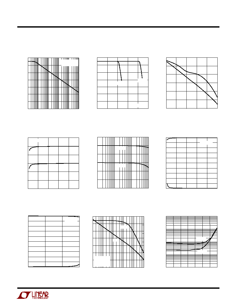
Gain/Phase vs Frequency
Bias Current vs Temperature
Output Swing vs Output Current
C
C
HARA TERISTICS
U
W
A
TYPICAL PERFOR
CE
Common Mode Rejection Ratio
vs Frequency
DC CMRR vs Common Mode Input
Voltage
Output Voltage Swing vs Load
Resistance
FREQUENCY (Hz)
20
CMRR (dB)
40
80
120
140
1
100
1k
100k
2050 G01
0
10
10k
60
100
V
S
= 3V OR 5V
V
CM
= 0.5V
P-P
V
CM
(V)
20
CMRR (dB)
40
80
120
140
1
3
4
0
2050 G02
0
2
5
60
100
V
S
= 3V
V
S
= 5V
T
A
= 25
°
C
LOAD RESISTANCE (k
)
0
OUTPUT SWING (V)
6
5
4
3
2
1
0
2
4
2050 G03
6
8
10
R
L
TO GND
V
S
= 5V
V
S
= 3V
OUTPUT CURRENT (mA)
0.01
2
OUTPUT VOLTAGE (V)
3
4
5
0.1
1
10
2050 G04
1
0
6
V
S
= 5V
V
S
= 3V
FREQUENCY (Hz)
0
GAIN (dB) 20
40
60
100
100
1k
100k
1M
10M
2050 G05
20
40
10k
80
180
PHASE (DEG)
160
140
120
100
200
80
GAIN
PHASE
V
S
= 3V OR 5V
C
L
= 35pF
R
L
= 10k
TEMPERATURE (
°
C)
25
10
1
100
10k
1k
100
75
2050 G06
50
125
BIAS CURRENT (pA)
50
0
25
V
S
= 3V
V
S
= 5V
FREQUENCY (Hz)
10
PSRR (dB)
120
100
80
60
40
20
0
100
1k
10k
100k
LTC2050 · G14
1M
PSRR
+PSRR
PSRR vs Frequency
LOAD RESISTANCE (k
)
0
OUTPUT SWING (V)
5
4
3
2
1
0
1
2
3
4
5
8
2050 G16
2
4
6
10
R
L
TO GND
OUTPUT CURRENT (mA)
0.01
OUTPUT SWING (V)
5
4
3
2
1
0
1
2
3
4
5
2050 G17
0.1
10
1.0
R
L
TO GND
Output Swing vs Output Current
±
5V Supply
Output Swing vs Load Resistance
±
5V Supply