Äîêóìåíòàöèÿ è îïèñàíèÿ www.docs.chipfind.ru
1
LTC2051
Dual Zero-Drift
Operational Amplifier
February 2000
s
Thermocouple Amplifiers
s
Electronic Scales
s
Medical Instrumentation
s
Strain Gauge Amplifiers
s
High Resolution Data Acquisition
s
DC Accurate RC Active Filters
U
S
A
O
PPLICATI
s
Maximum Offset Voltage of 3
µ
V
s
Maximum Offset Voltage Drift of 30nV/
°
C
s
Small Footprint, Low Profile MS8 Package
s
Noise: 1.5
µ
V
P-P
(0.1Hz to 10Hz Typ)
s
Voltage Gain: 140dB (Typ)
s
PSRR: 130dB (Typ)
s
CMRR: 130dB (Typ)
s
Supply Current: 0.75mA (Typ) per Amplifier
s
Single Supply Operation: 2.7V to 11V
s
Extended Common Mode Input Range
s
Output Swings Rail-to-Rail
s
Overload Recovery Time: 2ms (Typ)
s
Operating Temperature Range 40
°
C to 85
°
C
S
FEATURE
D
U
ESCRIPTIO
The LTC
®
2051 is a dual zero-drift operational amplifier
available in the MS8 and SO-8 packages. It operates from
a single 2.7V supply while still supporting
±
5V applica-
tions. The power consumption is 750
µ
A per op amp.
The LTC2051, despite its miniature size, features uncom-
promising DC performance. The typical input offset volt-
age and offset drift are 0.5
µ
V and 10nV/
°
C. The almost
zero DC offset and drift are supported with a power supply
rejection ratio (PSRR) and common mode rejection ratio
(CMRR) of more than 130dB.
The input common mode voltage ranges from the negative
supply up to 1V from the positive supply. The LTC2051
also has an enhanced output stage capable of driving
loads as low as 1k
to both supply rails. The open-loop
gain, loaded with 1k
, is in excess of 140dB. The LTC2051
also features a 1.5
µ
V
P-P
DC to 10Hz noise and a 3MHz gain
bandwidth product.
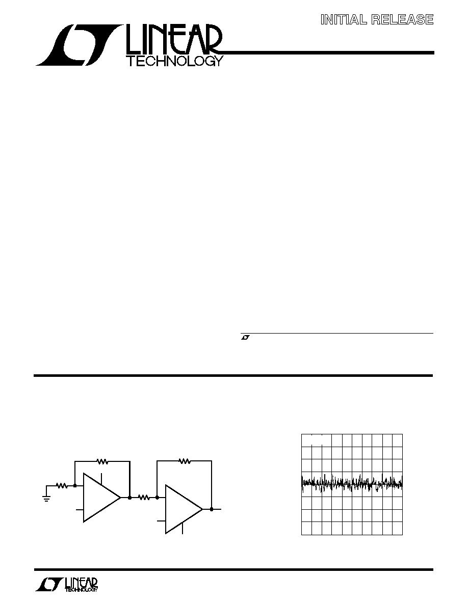
Input Referred Noise 0.1Hz to 10Hz
High Performance Low Cost Instrumentation Amplifier
U
A
O
PPLICATI
TYPICAL
, LTC and LT are registered trademarks of Linear Technology Corporation.
TIME (s)
0
µ
V
3
1
8
LT2051 TA02
0
1
3
2
4
6
10
V
S
= 5V
Information furnished by Linear Technology Corporation is believed to be accurate and reliable.
However, no responsibility is assumed for its use. Linear Technology Corporation makes no represen-
tation that the interconnection of its circuits as described herein will not infringe on existing patent rights.
+
R2
100k
0.1%
R1
499
0.1%
7
4
5
6
3
2
2051 TA01
5V
+
1/2
LTC2051HV
1/2
LTC2051HV
8
1
5V
V
IN
V
IN
A
V
= 201
R2
100k
0.1%
R1
499
0.1%
Final Electrical Specifications
2
LTC2051
: (LTC2051, LTC2051HV) The
q
denotes the specifications which apply over
the full operating temperature range, otherwise specifications are at T
A
= 25
°
C. V
S
= 3V, 5V unless otherwise noted. (Note 3)
W
U
U
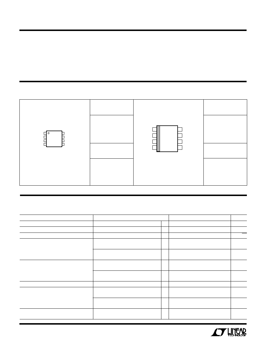
PACKAGE/ORDER I FOR ATIO
A
U
G
W
A
W
U
W
A
R
BSOLUTE
XI
TI
S
Total Supply Voltage (V
+
to V
)
LTC2051 .................................................................. 7V
LTC2051HV ........................................................... 12V
Input Voltage ........................ (V
+
+ 0.3V) to (V
0.3V)
Output Short-Circuit Duration ......................... Indefinite
Operating Temperature Range ............... 40
°
C to 85
°
C
Specified Temperature Range (Note 3) .. 40
°
C to 85
°
C
Storage Temperature Range ................ 65
°
C to 150
°
C
Lead Temperature (Soldering, 10 sec)................. 300
°
C
ELECTRICAL C
C
HARA TERISTICS
(Note 1)
Consult factory for Military grade parts.
ORDER PART
NUMBER
LTC2051CMS8
LTC2051IMS8
LTC2051HVCMS8
LTC2051HVIMS8
MS8 PART
MARKING
LTMN
LTMP
LTPJ
LTPK
ORDER PART
NUMBER
LTC2051CS8
LTC2051IS8
LTC2051HVCS8
LTC2051HVIS8
S8 PART
MARKING
2051
2051I
2051HV
051HVI
1
2
3
4
OUT A
IN A
+IN A
V
8
7
6
5
V
+
OUT B
IN B
+IN B
TOP VIEW
MS8 PACKAGE
8-LEAD PLASTIC MSOP
TOP VIEW
V
+
OUT B
IN B
+IN B
OUT A
IN A
+IN A
V
1
2
3
4
8
7
6
5
S8 PACKAGE
8-LEAD PLASTIC SO
T
JMAX
= 125
°
C,
JA
= 250
°
C/W
T
JMAX
= 125
°
C,
JA
= 190
°
C/W
PARAMETER
CONDITIONS
MIN
TYP
MAX
UNITS
Input Offset Voltage
(Note 2)
±
0.5
±
3
µ
V
Average Input Offset Drift
(Note 2)
q
±
0.03
µ
V/
°
C
Long-Term Offset Drift
50
nV/
mo
Input Bias Current
V
S
= 3V
±
8
±
50
pA
V
S
= 3V
q
±
100
pA
V
S
= 5V
±
25
±
75
pA
V
S
= 5V
q
±
150
pA
Input Offset Current
V
S
= 3V
±
100
pA
V
S
= 3V
q
±
150
pA
V
S
= 5V
±
150
pA
V
S
= 5V
q
±
200
pA
Input Noise Voltage
R
S
= 100
, DC to 10Hz
1.5
µ
V
P-P
Common Mode Rejection Ratio
V
CM
= V
to V
+
1.3, V
S
= 3V
115
130
dB
q
110
130
dB
V
CM
= V
to V
+
1.3, V
S
= 5V
120
130
dB
q
115
130
dB
Power Supply Rejection Ratio
120
130
dB
q
115
130
dB
3
LTC2051
PARAMETER
CONDITIONS
MIN
TYP
MAX
UNITS
Large-Signal Voltage Gain
R
L
= 10k, V
S
= 3V
120
140
dB
q
115
140
dB
R
L
= 10k, V
S
= 5V
125
140
dB
q
120
140
dB
Maximum Output Voltage Swing
R
L
= 2k
q
V
+
0.15
V
+
0.06
V
R
L
= 10k
q
V
+
0.05
V
+
0.02
V
Slew Rate
2
V/
µ
s
Gain Bandwidth Product
3
MHz
Supply Current (2 Amplifiers)
No Load, V
S
= 3V
q
1.5
2.0
mA
No Load, V
S
= 5V
q
1.7
2.4
mA
Internal Sampling Frequency
7.5
kHz
Note 1: Absolute Maximum Ratings are those values beyond which the life
of the device may be impaired.
Note 2: These parameters are guaranteed by design. Thermocouple effects
preclude measurements of these voltage levels during automated testing.
The
q
denotes the specifications which apply over the full operating temperature range, otherwise specifications are at T
A
= 25
°
C. V
S
=
±
5V unless otherwise noted. (Note 3) (LTC2051HV)
The
q
denotes the specifications which apply over the full operating
temperature range, otherwise specifications are at T
A
= 25
°
C. V
S
= 3V, 5V unless otherwise noted. (Note 3)
ELECTRICAL C
C
HARA TERISTICS
Note 3: The LTC2051C, LTC2051HVC is guaranteed to meet specified
performance from 0
°
C to 70
°
C and is designed, characterized and
expected to meet these extended temperature limits, but is not tested at
40
°
C and 85
°
C. The LTC2051I, LTC2051HVI is guaranteed to meet the
extended temperature limits.
PARAMETER
CONDITIONS
MIN
TYP
MAX
UNITS
Input Offset Voltage
(Note 2)
±
1
±
3
µ
V
Average Input Offset Drift
(Note 2)
q
±
0.03
µ
V/
°
C
Long-Term Offset Drift
50
nV/
mo
Input Bias Current
±
90
±
150
pA
q
±
300
pA
Input Offset Current
±
300
pA
q
±
500
pA
Input Noise Voltage
R
S
= 100
, DC to 10Hz
1.5
µ
V
P-P
Common Mode Rejection Ratio
V
CM
= V
to V
+
1.3
125
130
dB
q
120
130
dB
Power Supply Rejection Ratio
120
130
dB
q
115
130
dB
Large-Signal Voltage Gain
R
L
= 10k
125
140
dB
q
120
140
dB
Maximum Output Voltage Swing
R
L
= 2k
q
4.80
4.92
V
R
L
= 10k
q
4.95
4.98
V
Slew Rate
2
V/
µ
s
Gain Bandwidth Product
3
MHz
Supply Current (2 Amplifiers)
No Load
q
2
3
mA
Internal Sampling Frequency
7.5
kHz
4
LTC2051
©
LINEAR TECHNOLOGY CORPORATION 2000
2051i LT/TP 0200 4K · PRINTED IN USA
Linear Technology Corporation
1630 McCarthy Blvd., Milpitas, CA 95035-7417
(408) 432-1900
q
FAX: (408) 434-0507
q
www.linear-tech.com
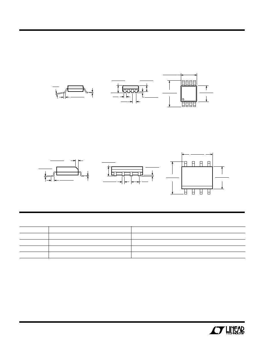
PACKAGE DESCRIPTIO
N
U
Dimensions in inches (millimeters) unless otherwise noted.
RELATED PARTS
PART NUMBER
DESCRIPTION
COMMENTS
LTC1051/LTC1053
Precision Zero-Drift Op Amp
Dual/Quad
LTC1151
±
15V Zero-Drift Op Amp
Dual High Voltage Operation
±
18V
LTC1152
Rail-to-Rail Input and Output Zero-Drift Op Amp
Single Zero-Drift Op Amp with Rail-to-Rail Input and Output and Shutdown
LTC2050
Zero-Drift Op Amp in SOT-23
Single Supply Operation 2.7V to 6V, Shutdown
MSOP (MS8) 1098
* DIMENSION DOES NOT INCLUDE MOLD FLASH, PROTRUSIONS OR GATE BURRS. MOLD FLASH,
PROTRUSIONS OR GATE BURRS SHALL NOT EXCEED 0.006" (0.152mm) PER SIDE
** DIMENSION DOES NOT INCLUDE INTERLEAD FLASH OR PROTRUSIONS.
INTERLEAD FLASH OR PROTRUSIONS SHALL NOT EXCEED 0.006" (0.152mm) PER SIDE
0.021
±
0.006
(0.53
±
0.015)
0
°
6
°
TYP
SEATING
PLANE
0.007
(0.18)
0.040
±
0.006
(1.02
±
0.15)
0.012
(0.30)
REF
0.006
±
0.004
(0.15
±
0.102)
0.034
±
0.004
(0.86
±
0.102)
0.0256
(0.65)
BSC
1
2
3
4
0.193
±
0.006
(4.90
±
0.15)
8
7 6
5
0.118
±
0.004*
(3.00
±
0.102)
0.118
±
0.004**
(3.00
±
0.102)
MS8 Package
8-Lead Plastic MSOP
(LTC DWG # 05-08-1660)
S8 Package
8-Lead Plastic Small Outline (Narrow 0.150)
(LTC DWG # 05-08-1610)
SO8 0996
0.016 0.050
(0.406 1.270)
0.010 0.020
(0.254 0.508)
×
45
°
0
°
8
°
TYP
0.008 0.010
(0.203 0.254)
0.053 0.069
(1.346 1.752)
0.014 0.019
(0.355 0.483)
0.004 0.010
(0.101 0.254)
0.050
(1.270)
TYP
1
2
3
4
0.150 0.157**
(3.810 3.988)
8
7
6
5
0.189 0.197*
(4.801 5.004)
0.228 0.244
(5.791 6.197)
DIMENSION DOES NOT INCLUDE MOLD FLASH. MOLD FLASH
SHALL NOT EXCEED 0.006" (0.152mm) PER SIDE
DIMENSION DOES NOT INCLUDE INTERLEAD FLASH. INTERLEAD
FLASH SHALL NOT EXCEED 0.010" (0.254mm) PER SIDE
*
**