 | ÐлекÑÑоннÑй компоненÑ: LTC2052HV | СкаÑаÑÑ:  PDF PDF  ZIP ZIP |
20512fa.pm6
1
LTC2051/LTC2052
20512fb
Dual/Quad Zero-Drift
Operational Amplifiers
s
Thermocouple Amplifiers
s
Electronic Scales
s
Medical Instrumentation
s
Strain Gauge Amplifiers
s
High Resolution Data Acquisition
s
DC Accurate RC Active Filters
s
Low Side Current Sense
s
Maximum Offset Voltage of 3
µ
V
s
Maximum Offset Voltage Drift of 30nV/
°
C
s
Small Footprint, Low Profile MS8/GN16 Packages
s
Available in 3mm
×
3mm
×
0.8mm DFN Package
s
Single Supply Operation: 2.7V to
±
5.5V
s
Noise: 1.5
µ
V
P-P
(0.01Hz to 10Hz Typ)
s
Voltage Gain: 140dB (Typ)
s
PSRR: 130dB (Typ)
s
CMRR: 130dB (Typ)
s
Supply Current: 0.75mA (Typ) per Amplifier
s
Extended Common Mode Input Range
s
Output Swings Rail-to-Rail
s
Operating Temperature Range 40
°
C to 125
°
C
The LTC
®
2051/LTC2052 are dual/quad zero-drift opera-
tional amplifiers available in the MS8 and SO-8/GN16 and
S14 packages. For space limited applications, the LTC2051
is available in a 3mm
×
3mm
×
0.8mm dual fine pitch
leadless package (DFN). They operate from a single 2.7V
supply and support
±
5V applications. The current con-
sumption is 750
µ
A per op amp.
The LTC2051/LTC2052, despite their miniature size, fea-
ture uncompromising DC performance. The typical input
offset voltage and offset drift are 0.5
µ
V and 10nV/
°
C. The
almost zero DC offset and drift are supported with a power
supply rejection ratio (PSRR) and common mode rejec-
tion ratio (CMRR) of more than 130dB.
The input common mode voltage ranges from the negative
supply up to typically 1V from the positive supply. The
LTC2051/LTC2052 also have an enhanced output stage
capable of driving loads as low as 2k
to both supply rails.
The open-loop gain is typically 140dB. The LTC2051/
LTC2052 also feature a 1.5
µ
V
P-P
DC to 10Hz noise and a
3MHz gain-bandwidth product.
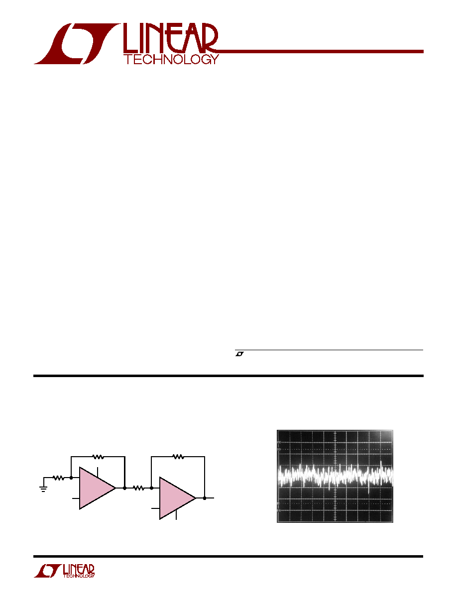
Input Referred Noise 0.1Hz to 10Hz
High Performance Low Cost Instrumentation Amplifier
, LTC and LT are registered trademarks of Linear Technology Corporation.
2
1
0
1
2
µ
V
0
2
4
6
8
10
TIME (SEC)
2052 TA02
FEATURES
DESCRIPTIO
U
APPLICATIO S
U
TYPICAL APPLICATIO
U
+
R2
10k
0.1%
R1
100
0.1%
7
4
5
6
3
2
20512 TA01
5V
+
1/2
LTC2051HV
1/2
LTC2051HV
8
1
5V
V
IN
V
IN
A
V
= 101
R2
10k
0.1%
R1
100
0.1%
2
LTC2051/LTC2052
20512fb
Total Supply Voltage (V
+
to V
)
LTC2051/LTC2052 .................................................. 7V
LTC2051HV/LTC2052HV ....................................... 12V
Input Voltage (Note 5) .......... (V
+
+ 0.3V) to (V
0.3V)
Output Short-Circuit Duration ......................... Indefinite
Operating Temperature Range ............. 40
°
C to 125
°
C
Specified Temperature Range (Note 3) 40
°
C to 125
°
C
Storage Temperature Range ................ 65
°
C to 150
°
C
DD Package ...................................... 65
°
C to 125
°
C
Lead Temperature (Soldering, 10 sec)................. 300
°
C
(Note 1)
ORDER PART
NUMBER
ABSOLUTE AXI U RATI GS
W
W
W
U
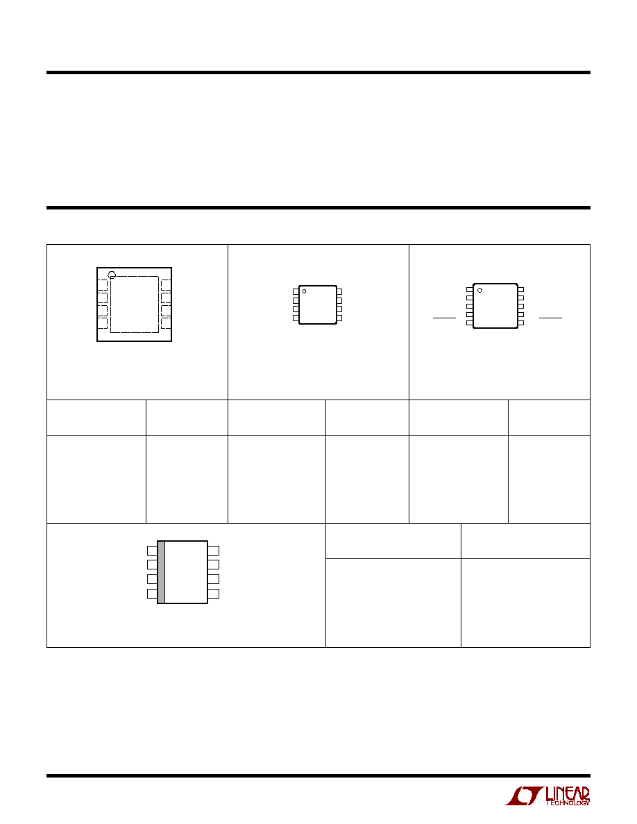
PACKAGE/ORDER I FOR ATIO
U
U
W
T
JMAX
= 125
°
C,
JA
= 190
°
C/W
1
2
3
4
OUT A
IN A
+IN A
V
8
7
6
5
V
+
OUT B
IN B
+IN B
TOP VIEW
MS8 PACKAGE
8-LEAD PLASTIC MSOP
1
2
3
4
5
OUT A
IN A
+IN A
V
SHDN A
10
9
8
7
6
V
+
OUT B
IN B
+IN B
SHDN B
TOP VIEW
MS10 PACKAGE
10-LEAD PLASTIC MSOP
TOP VIEW
V
+
OUT B
IN B
+IN B
OUT A
IN A
+IN A
V
1
2
3
4
8
7
6
5
S8 PACKAGE
8-LEAD PLASTIC SO
T
JMAX
= 125
°
C,
JA
= 250
°
C/W
T
JMAX
= 125
°
C,
JA
= 250
°
C/W
MS8 PART
MARKING
LTC2051CMS8
LTC2051IMS8
LTC2051HVCMS8
LTC2051HVIMS8
LTC2051HMS8
LTC2051HVHMS8
LTMN
LTMP
LTPJ
LTPK
LTVF
LTVH
ORDER PART
NUMBER
MS10 PART
MARKING
LTC2051CMS10
LTC2051IMS10
LTC2051HVCMS10
LTC2051HVIMS10
LTMQ
LTMR
LTRB
LTRC
ORDER PART
NUMBER
S8 PART
MARKING
LTC2051CS8
LTC2051IS8
LTC2051HVCS8
LTC2051HVIS8
LTC2051HS8
LTC2051HVHS8
2051
2051I
2051HV
051HVI
2051H
051HVH
*The temperature grade (I or C) of the LTC2051's packaged in DFNs is indicated on the shipping container. Consult LTC Marketing for parts specified with
wider operating temperature ranges.
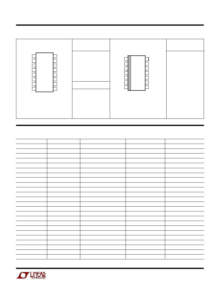
TOP VIEW
DD PACKAGE
8-LEAD (3mm
×
3mm) PLASTIC DFN
5
6
7
8
4
3
2
1
OUT A
IN A
+IN A
V
V
+
OUT B
IN B
+IN B
T
JMAX
= 125
°
C,
JA
= 160
°
C/W
ORDER PART
NUMBER*
DD PART
MARKING
LTC2051CDD
LTC2051IDD
LTC2051HVCDD
LTC2051HVIDD
LAAN
LAEL
3
LTC2051/LTC2052
20512fb
AVAILABLE OPTIO S
U
PART NUMBER
AMPS/PACKAGE
SPECIFIED TEMP RANGE
SPECIFIED VOLTAGE
PACKAGE
LTC2051CDD
2
0
°
C to 70
°
C
3V, 5V
DD
LTC2051CS8
2
0
°
C to 70
°
C
3V, 5V
SO-8
LT2051CMS8
2
0
°
C to 70
°
C
3V, 5V
8-Lead MSOP
LT2051CMS10
2
0
°
C to 70
°
C
3V, 5V
10-Lead MSOP
LTC2051HVCDD
2
0
°
C to 70
°
C
3V, 5V,
±
5V
DD
LT2051HVCS8
2
0
°
C to 70
°
C
3V, 5V,
±
5V
SO-8
LTC2051HVCMS8
2
0
°
C to 70
°
C
3V, 5V,
±
5V
8-Lead MSOP
LTC2051HVCMS10
2
0
°
C to 70
°
C
3V, 5V,
±
5V
10-Lead MSOP
LTC2051IDD
2
40
°
C to 85
°
C
3V, 5V
DD
LTC2051IS8
2
40
°
C to 85
°
C
3V, 5V
SO-8
LT2051IMS8
2
40
°
C to 85
°
C
3V, 5V
8-Lead MSOP
LT2051IMS10
2
40
°
C to 85
°
C
3V, 5V
10-Lead MSOP
LTC2051HVIDD
2
40
°
C to 85
°
C
3V, 5V,
±
5V
DD
LT2051HVIS8
2
40
°
C to 85
°
C
3V, 5V,
±
5V
SO-8
LTC2051HVIMS8
2
40
°
C to 85
°
C
3V, 5V,
±
5V
8-Lead MSOP
LTC2051HVIMS10
2
40
°
C to 85
°
C
3V, 5V,
±
5V
10-Lead MSOP
LTC2051HS8
2
40
°
C to 125
°
C
3V, 5V
SO-8
LT2051HMS8
2
40
°
C to 125
°
C
3V, 5V
8-Lead MSOP
LT2051HVHS8
2
40
°
C to 125
°
C
3V, 5V,
±
5V
SO-8
LT2051HVHMS8
2
40
°
C to 125
°
C
3V, 5V,
±
5V
8-Lead MSOP
LTC2052CS
4
0
°
C to 70
°
C
3V, 5V
14-Lead SO
LTC2052CGN
4
0
°
C to 70
°
C
3V, 5V
16-Lead SSOP
LTC2052HVCS
4
0
°
C to 70
°
C
3V, 5V,
±
5V
14-Lead SO
LTC2052HVCGN
4
0
°
C to 70
°
C
3V, 5V,
±
5V
16-Lead SSOP
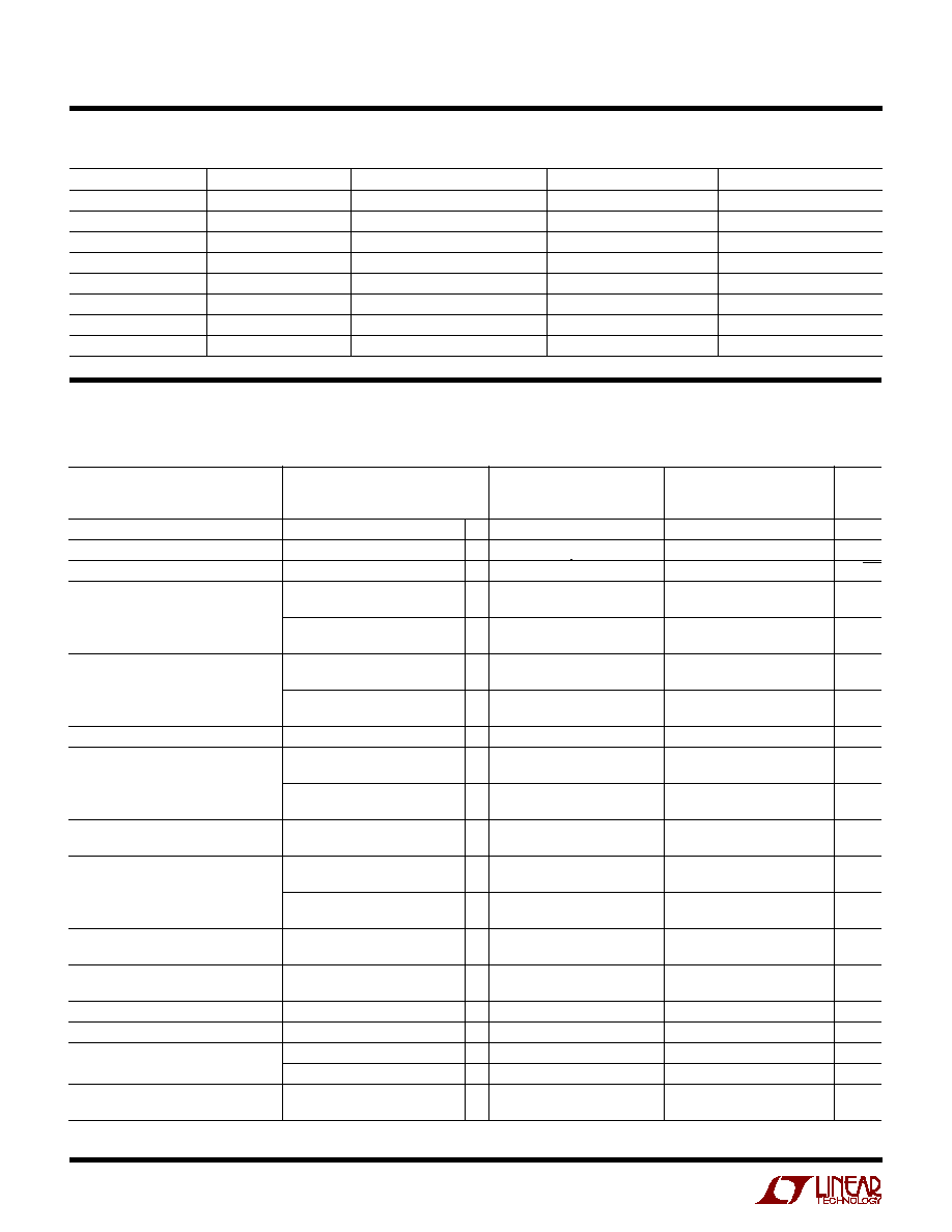
GN PACKAGE
16-LEAD PLASTIC SSOP
1
2
3
4
5
6
7
8
TOP VIEW
16
15
14
13
12
11
10
9
OUT A
IN A
+IN A
V
+
+IN B
IN B
OUT B
NC
OUT D
IN D
+IN D
V
+IN C
IN C
OUT C
NC
ORDER PART
NUMBER
LTC2052CGN
LTC2052IGN
LTC2052HVCGN
LTC2052HVIGN
LTC2052HGN
LTC2052HVHGN
T
JMAX
= 125
°
C,
JA
= 110
°
C/W
GN PART MARKING
2052
2052I
2052HV
052HVI
2052H
052HVH
TOP VIEW
S PACKAGE
14-LEAD PLASTIC SO
1
2
3
4
5
6
7
14
13
12
11
10
9
8
OUT A
IN A
+IN A
V
+
+IN B
IN B
OUT B
OUT D
IN D
+IN D
V
+IN C
IN C
OUT C
T
JMAX
= 125
°
C,
JA
= 110
°
C/W
ORDER PART
NUMBER
LTC2052CS
LTC2052IS
LTC2052HVCS
LTC2052HVIS
LTC2052HS
LTC2052HVHS
PACKAGE/ORDER I FOR ATIO
U
U
W
4
LTC2051/LTC2052
20512fb
LTC2051C/LTC2052C
LTC2051I/LTC2052I
LTC2051H/LTC2052H
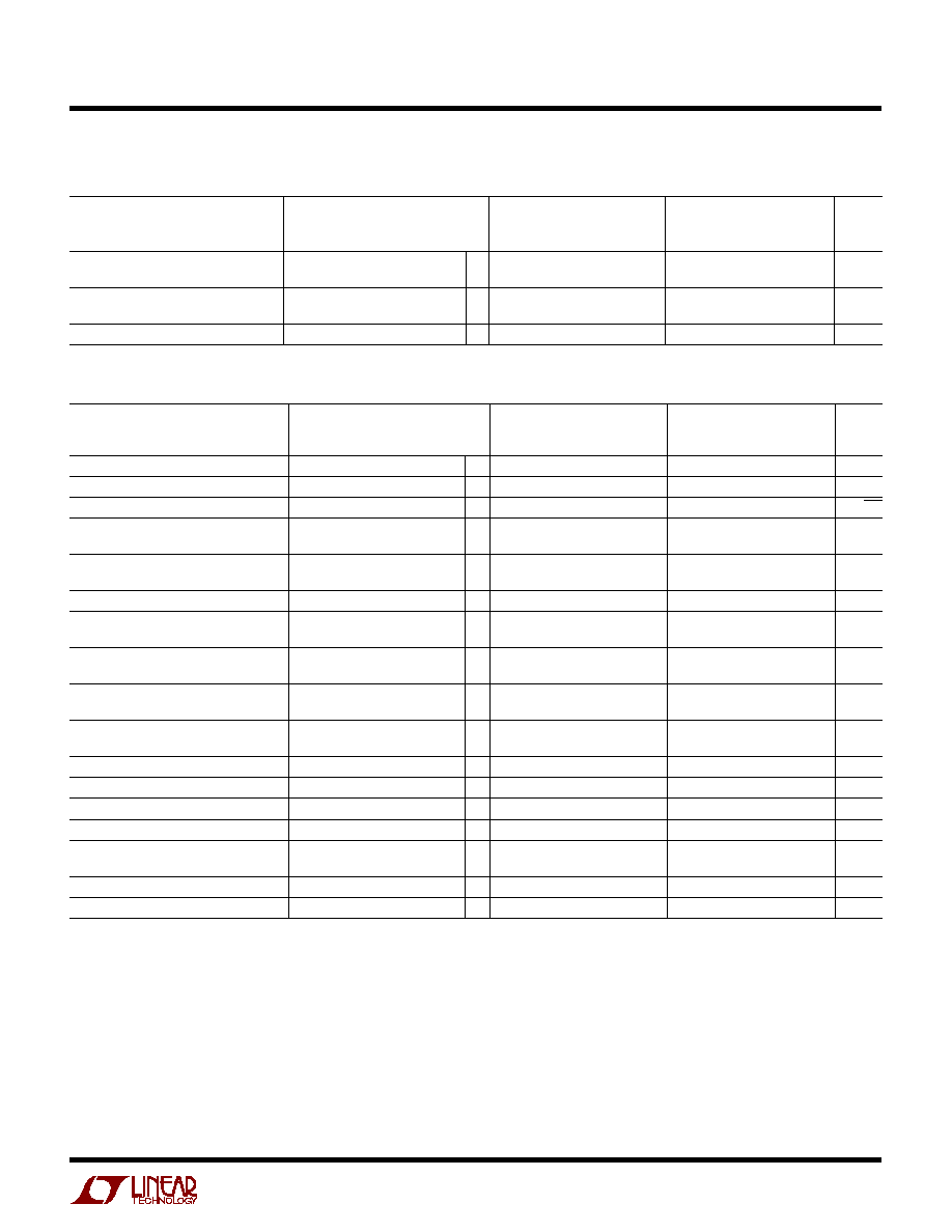
PARAMETER
CONDITIONS
MIN
TYP
MAX
MIN
TYP
MAX
UNITS
Input Offset Voltage
(Note 2)
±
0.5
±
3
±
0.5
±
3
µ
V
Average Input Offset Drift
(Note 2)
q
0.01
±
0.03
0.01
±
0.05
µ
V/
°
C
Long-Term Offset Drift
50
50
nV/
mo
Input Bias Current (Note 4)
V
S
= 3V
±
8
±
50
±
8
±
50
pA
V
S
= 3V
q
±
100
±
3000
pA
V
S
= 5V
±
25
±
75
±
25
±
75
pA
V
S
= 5V
q
±
150
±
3000
pA
Input Offset Current (Note 4)
V
S
= 3V
±
100
±
100
pA
V
S
= 3V
q
±
150
±
700
pA
V
S
= 5V
±
150
±
150
pA
V
S
= 5V
q
±
200
±
700
pA
Input Noise Voltage
R
S
= 100
, DC to 10Hz
1.5
1.5
µ
V
P-P
Common Mode Rejection Ratio
V
CM
= GND to V
+
1.3,
115
130
115
130
dB
V
S
= 3V
q
110
130
110
130
dB
V
CM
= GND to V
+
1.3,
120
130
120
130
dB
V
S
= 5V
q
115
130
115
130
dB
Power Supply Rejection Ratio
120
130
120
130
dB
q
115
130
115
130
dB
Large-Signal Voltage Gain
R
L
= 10k, V
S
= 3V
120
140
120
140
dB
q
115
140
115
140
dB
R
L
= 10k, V
S
= 5V
125
140
125
140
dB
q
120
140
120
140
dB
Output Voltage Swing High
R
L
= 2k to GND
q
V
+
0.15 V
+
0.06
V
+
0.15 V
+
0.06
V
R
L
= 10k to GND
q
V
+
0.05 V
+
0.02
V
+
0.05 V
+
0.02
V
Output Voltage Swing Low
R
L
= 2k to GND
q
2
15
2
15
mV
R
L
= 10k to GND
q
2
15
2
15
mV
Slew Rate
2
2
V/
µ
s
Gain Bandwidth Product
3
3
MHz
Supply Current (Per Amplifier)
No Load, V
S
= 3V, V
SHDN
= V
IH
q
0.75
1.0
0.75
1.1
mA
No Load, V
S
= 5V, V
SHDN
= V
IH
q
0.85
1.2
0.85
1.3
mA
Supply Current, Shutdown
V
SHDN
= V
IL
, V
S
= 3V
q
2
5
2
5
µ
A
V
SHDN
= V
IL
, V
S
= 5V
q
4
10
4
10
µ
A
(LTC2051/LTC2052, LTC2051HV/LTC2052HV) The
q
denotes the
specifications which apply over the full operating temperature range, otherwise specifications are at T
A
= 25
°
C. V
S
= 3V, 5V
unless otherwise noted. (Note 3)
ELECTRICAL CHARACTERISTICS
AVAILABLE OPTIO S
U
LTC2052IS
4
40
°
C to 85
°
C
3V, 5V
14-Lead SO
LTC2052IGN
4
40
°
C to 85
°
C
3V, 5V
16-Lead SSOP
LTC2052HVIS
4
40
°
C to 85
°
C
3V, 5V,
±
5V
14-Lead SO
LTC2052HVIGN
4
40
°
C to 85
°
C
3V, 5V,
±
5V
16-Lead SSOP
LTC2052HS
4
40
°
C to 125
°
C
3V, 5V
14-Lead SO
LTC2052HGN
4
40
°
C to 125
°
C
3V, 5V
16-Lead SSOP
LTC2052HVHS
4
40
°
C to 125
°
C
3V, 5V,
±
5V
14-Lead SO
LTC2052HVHGN
4
40
°
C to 125
°
C
3V, 5V,
±
5V
16-Lead SSOP
PART NUMBER
AMPS/PACKAGE
SPECIFIED TEMP RANGE
SPECIFIED VOLTAGE
PACKAGE
5
LTC2051/LTC2052
20512fb
ELECTRICAL CHARACTERISTICS
LTC2051C/LTC2052C
LTC2051I/LTC2052I
LTC2051H/LTC2052H
PARAMETER
CONDITIONS
MIN
TYP
MAX
MIN
TYP
MAX
UNITS
(LTC2051/LTC2052, LTC2051HV/LTC2052HV) The
q
denotes the
specifications which apply over the full operating temperature range, otherwise specifications are at T
A
= 25
°
C. V
S
= 3V, 5V
unless otherwise noted. (Note 3)
Shutdown Pin Input Low Voltage (V
IL
)
q
V
+ 0.5
V
+ 0.5
V
Shutdown Pin Input High Voltage (V
IH
)
q
V
+
0.5
V
+
0.5
V
Shutdown Pin Input Current
V
SHDN
= V
IL
, V
S
= 3V
q
1
3
1
3
µ
A
V
SHDN
= V
IL
, V
S
= 5V
q
2
5
2
5
µ
A
Internal Sampling Frequency
7.5
7.5
kHz
LTC2051C/LTC2052C
LTC2051I/LTC2052I
LTC2051H/LTC2052H
PARAMETER
CONDITIONS
MIN
TYP
MAX
MIN
TYP
MAX
UNITS
Input Offset Voltage
(Note 2)
±
1
±
3
±
1
±
3
µ
V
Average Input Offset Drift
(Note 2)
q
0.01
±
0.03
0.01
±
0.05
µ
V/
°
C
Long-Term Offset Drift
50
50
nV/
mo
Input Bias Current (Note 4)
±
90
±
150
±
90
±
150
pA
q
±
300
±
3000
pA
Input Offset Current (Note 4)
±
300
±
300
pA
q
±
500
±
700
pA
Input Noise Voltage
R
S
= 100
, DC to 10Hz
1.5
1.5
µ
V
P-P
Common Mode Rejection Ratio
V
CM
= V
to V
+
1.3
125
130
125
130
dB
q
120
130
120
130
dB
Power Supply Rejection Ratio
120
130
120
130
dB
q
115
130
115
130
dB
Large-Signal Voltage Gain
R
L
= 10k
125
140
125
140
dB
q
120
140
120
140
dB
Maximum Output Voltage Swing
R
L
= 2k to GND
q
±
4.75
±
4.92
±
4.50
±
4.92
V
R
L
= 10k to GND
q
±
4.90
±
4.98
±
4.85
±
4.98
V
Slew Rate
2
2
V/
µ
s
Gain Bandwidth Product
3
3
MHz
Supply Current (Per Amplifier)
No Load, V
SHDN
= V
IH
q
1
1.5
1
1.5
mA
Supply Current, Shutdown
V
SHDN
= V
IL
q
15
30
15
30
µ
A
Shutdown Pin Input Low Voltage (V
IL
)
q
V
+ 0.5
V
+ 0.5
V
Shutdown Pin Input High Voltage (V
IH
)
q
V
+
0.5
V
+
0.5
V
Shutdown Pin Input Current
V
SHDN
= V
IL
q
7
15
7
15
µ
A
Internal Sampling Frequency
7.5
7.5
kHz
Note 1: Absolute Maximum Ratings are those values beyond which the life
of the device may be impaired.
Note 2: These parameters are guaranteed by design. Thermocouple effects
preclude measurements of these voltage levels during automated testing.
Note 3: All versions of the LTC2051/LTC2052 are designed, characterized
and expected to meet the extended temperature limits of 40
°
C and
125
°
C. The LTC2051C/LTC2052C/LTC2051HVC/LTC2052HVC are
guaranteed to meet the temperature limits of 0
°
C and 70
°
C. The LTC2051I/
LTC2052I/LTC2051HVI/LTC2052HVI are guaranteed to meet temperature
limits of 40
°
C and 85
°
C. The LTC2051H/LTC2051HVH and LTC2052H/
LTC2052HVH are guaranteed to meet the temperature limits of 40
°
C and
125
°
C.
(LTC2051HV/LTC2052HV) The
q
denotes the specifications which apply over the full operating temperature range, otherwise
specifications are at T
A
= 25
°
C. V
S
=
±
5V unless otherwise noted. (Note 3)
Note 4: The bias current measurement accuracy depends on the proximity
of the negative supply bypass capacitors to the device under test. Because
of this, only the bias current of channel B (LTC2051) and channels A and B
(LTC2052) are 100% tested to the data sheet specifications. The bias
currents of the remaining channels are 100% tested to relaxed limits,
however, their values are guaranteed by design to meet the data sheet
limits.
Note 5: This parameter is guaranteed to meet specified performance
through design and characterization. It has not been tested.
Note 6: The
JA
specified for the DD package is with minimal PCB heat
spreading metal. Using expanded metal area on all layers of a board
reduces this value.