1
LTC2054/LTC2054HV
2054f
TEMPERATURE (
∞
C)
≠45
SUPPLY CURRENT (
µ
A)
250
225
200
175
150
125
100
75
50
25
0
≠5
2054 TA02
35
15
≠25
55
75
V
S
=
±
5V
V
S
=
±
2.5V
V
S
=
±
1.5V
APPLICATIO S
U
DESCRIPTIO
U
FEATURES
TYPICAL APPLICATIO
N
U
Low Power Zero-Drift
Operational Amplifiers
in SOT-23
s
Thermocouple Amplifiers
s
Electronic Scales
s
Medical Instrumentation
s
Strain Gauge Amplifiers
s
High Resolution Data Acquisition
s
DC Accurate RC Active Filters
s
Low Side Current Sense
s
Battery-Powered Systems
s
Supply Current 175
µ
A (Max), Guaranteed
Over Temperature
s
Offset Voltage 3
µ
V (Max)
s
Offset Voltage Drift 30nV/
∞
C (Max)
s
Noise: 1.6
µ
V
P-P
(0.01Hz to 10Hz Typ)
s
Voltage Gain: 140dB (Typ)
s
PSRR: 130dB (Typ)
s
CMRR: 130dB (Typ)
s
Input Bias Current <1pA (Typ)
s
Supply Operation: 2.7V to 6V (LTC2054)
2.7V to
±
5.5V (LTC2054HV)
s
Common Mode Input Range from V
≠
to V
+
≠0.5V
s
Output Swings Rail-to-Rail
s
Low Profile (1mm) SOT-23 (ThinSOTTM) Package
The LTC
Æ
2054 and LTC2054HV are low power, low noise
zero-drift operational amplifiers available in the
5-lead SOT-23 package. The LTC2054 operates from a
single 2.7V to 6V supply. The LTC2054HV operates on
supplies from 2.7V to
±
5.5V. The current consumption is
150
µ
A (typical), 175
µ
A maximum over temperature.
The LTC2054, despite its miniature size, features uncom-
promising DC performance. The typical input offset volt-
age and offset drift are 0.5
µ
V and 25nV/
∞
C. The almost
zero DC offset and drift are supported with a power supply
rejection ratio (PSRR) and common mode rejection ratio
(CMRR) of more than 130dB.
The input common mode voltage ranges from the negative
supply up to typically 0.5V from the positive supply. The
open-loop gain is typically 140dB. The LTC2054 also
features a 1.6
µ
V
P-P
DC to 10Hz noise and a 500kHz gain
bandwidth product.
Supply Current vs
Temperature
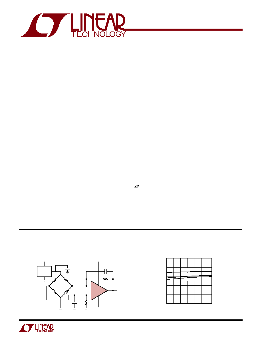
Differential Bridge Amplifier
, LTC and LT are registered trademarks of Linear Technology Corporation.
≠
+
5V
0.1
µ
F
499k
0.1
µ
F
499k
5
1
2
3
4
1
µ
F
5V
A
V
= 100
2054 TA01
10k
BRIDGE
LTC2054HV
≠ 5V
LT1790-2.5
ThinSOT is a trademark of Linear Technology Corporation.
2
LTC2054/LTC2054HV
2054f
A
U
G
W
A
W
U
W
A
R
BSOLUTE
XI
TI
S
Total Supply Voltage (V
+
to V
≠
)
LTC2054 .............................................................. 7V
LTC2054HV ......................................................... 12V
Input Voltage ........................ (V
+
+ 0.3V) to (V
≠
≠ 0.3V)
Output Short-Circuit Duration ......................... Indefinite
Operating Temperature Range ............... ≠ 40
∞
C to 85
∞
C
Specified Temperature Range
(Note 4) ................................................. ≠ 40
∞
C to 85
∞
C
Storage Temperature Range ................ ≠ 65
∞
C to 150
∞
C
Lead Temperature (Soldering, 10 sec)................. 300
∞
C
(Note 1)
(LTC2054, LTC2054HV) The
q
denotes specifications which apply over the
full operating temperature range, otherwise specifications are at T
A
= 25
∞
C. V
S
= 3V unless otherwise noted. (Note 4)
ELECTRICAL C
C
HARA TERISTICS
SYMBOL
PARAMETER
CONDITIONS
MIN
TYP
MAX
UNITS
I
S
Supply Current
No Load
q
140
175
µ
A
V
OS
Input Offset Voltage
(Note 2)
±
0.5
±
3
µ
V
V
OS
/
T
Average Input Offset Drift
(Note 2)
q
±
0.03
µ
V/
∞
C
Long-Term Offset Drift
50
nV/
mo
I
B
Input Bias Current
(Note 3)
±
600
fA
q
±
150
pA
I
OS
Input Offset Current
(Note 3)
±
1.2
pA
q
±
300
pA
e
n
Input Noise Voltage
R
S
= 100
, 0.01Hz to 10Hz
1.6
µ
V
P-P
CMRR
Common Mode Rejection Ratio
V
CM
= GND to (V
+
≠ 0.7V)
115
130
dB
q
110
dB
PSRR
Power Supply Rejection Ratio
V
S
= 2.7V to 6V
120
130
dB
q
115
dB
W
U
U
PACKAGE/ORDER I FOR ATIO
Consult LTC Marketing for parts specified with wider operating temperature ranges.
ORDER PART
NUMBER
LTC2054CS5
LTC2054HVCS5
LTC2054IS5
LTC2054HVIS5
S5 PART
MARKING
OUT 1
V
≠
2
TOP VIEW
S5 PACKAGE
5-LEAD PLASTIC TSOT-23
+IN 3
5 V
+
4 ≠IN
T
JMAX
= 150
∞
C,
JA
= 250
∞
C/W
LTAGB
LTAGD
LTAGB
LTAGD
3
LTC2054/LTC2054HV
2054f
SYMBOL
PARAMETER
CONDITIONS
MIN
TYP
MAX
UNITS
I
S
Supply Current
No Load
q
150
175
µ
A
V
OS
Input Offset Voltage
(Note 2)
±
3
µ
V
V
OS
/
T
Average Input Offset Drift
(Note 2)
q
±
0.03
µ
V/
∞
C
Long-Term Offset Drift
50
nV/
mo
I
B
Input Bias Current
(Note 3)
±
800
fA
q
±
150
pA
I
OS
Input Offset Current
(Note 3)
±
1.6
pA
q
±
300
pA
e
n
Input Noise Voltage
R
S
= 100
, 0.01Hz to 10Hz
1.6
µ
V
P-P
CMRR
Common Mode Rejection Ratio
V
CM
= GND to (V
+
≠ 0.7V)
120
130
dB
q
115
dB
PSRR
Power Supply Rejection Ratio
V
S
= 2.7V to 6V
120
130
dB
q
115
dB
A
VOL
Large-Signal Voltage Gain
R
L
= 100k, V
OUT
= V
S
/2
125
140
dB
q
120
dB
V
OUT
Output Voltage Swing High
R
L
= 5k to GND
q
4.75
V
R
L
= 100k to GND
q
4.98
V
V
OUT
Output Voltage Swing Low
R
L
= 5k to GND
q
10
mV
R
L
= 100k to GND
q
10
mV
SR
Slew Rate
0.5
V/
µ
s
GBW
Gain Bandwidth Product
500
kHz
f
S
Internal Sampling Frequency
1.0
kHz
(LTC2054, LTC2054HV) V
S
= 5V unless otherwise noted. (Note 4)
SYMBOL
PARAMETER
CONDITIONS
MIN
TYP
MAX
UNITS
A
VOL
Large-Signal Voltage Gain
R
L
= 100k, V
OUT
= V
S
/2
120
135
dB
q
115
dB
V
OUT
Output Voltage Swing High
R
L
= 5k to GND
q
2.85
V
R
L
= 100k to GND
q
2.98
V
V
OUT
Output Voltage Swing Low
R
L
= 5k to GND
q
10
mV
R
L
= 100k to GND
q
10
mV
SR
Slew Rate
0.5
V/
µ
s
GBW
Gain Bandwidth Product
500
kHz
f
S
Internal Sampling Frequency
1.0
kHz
(LTC2054, LTC2054HV) The
q
denotes specifications which apply over the
full operating temperature range, otherwise specifications are at T
A
= 25
∞
C. V
S
= 3V unless otherwise noted. (Note 4)
ELECTRICAL C
C
HARA TERISTICS
4
LTC2054/LTC2054HV
2054f
Note 1: Absolute Maximum Ratings are those values beyond which the life
of the device may be impaired.
Note 2: These parameters are guaranteed by design. Thermocouple effects
preclude measurements of these voltage levels during automated testing.
Note 3: Limit is determined by high speed automated test capability. See
characteristic curves for actual typical performance. For tighter
specifications, please consult Linear Technology Marketing.
(LTC2054HV) The
q
denotes specifications which apply over the full
operating temperature range, otherwise specifications are at T
A
= 25
∞
C. V
S
=
±
5V unless otherwise noted. (Note 4)
ELECTRICAL C
C
HARA TERISTICS
SYMBOL
PARAMETER
CONDITIONS
MIN
TYP
MAX
UNITS
I
S
Supply Current
No Load
q
175
210
µ
A
V
OS
Input Offset Voltage
(Note 2)
±
0.5
±
5
µ
V
V
OS
/
T
Average Input Offset Drift
(Note 2)
q
±
0.03
µ
V/
∞
C
Long-Term Offset Drift
50
nV/
mo
I
B
Input Bias Current
(Note 3)
±
1
pA
q
±
150
pA
I
OS
Input Offset Current
(Note 3)
±
2
pA
q
±
300
pA
e
n
Input Noise Voltage
R
S
= 100
, 0.01Hz to 10Hz
1.6
µ
V
P-P
CMRR
Common Mode Rejection Ratio
V
CM
= V
≠
to (V
+
≠ 0.9V)
120
130
dB
q
115
dB
PSRR
Power Supply Rejection Ratio
V
S
= 2.7V to 11V
120
130
dB
q
115
dB
A
VOL
Large-Signal Voltage Gain
R
L
= 100k, V
OUT
= GND
125
140
dB
q
120
dB
V
OUT
Maximum Output Voltage Swing
R
L
= 5k to GND
q
±
4.75
V
R
L
= 100k to GND
q
±
4.98
V
SR
Slew Rate
0.5
V/
µ
s
GBW
Gain Bandwidth Product
500
kHz
f
S
Internal Sampling Frequency
1.0
kHz
Note 4: The LTC2054C, LTC2054HVC are guaranteed to meet specified
performance from 0
∞
C to 70
∞
C and are designed, characterized and
expected to meet these extended temperature limits, but are not tested at
≠40
∞
C and 85
∞
C. The LTC2054I, LTC2054HVI are guaranteed to meet the
specified performance from ≠40
∞
C and 85
∞
C.
5
LTC2054/LTC2054HV
2054f
OUTPUT CURRENT (mA)
0
OUTPUT SWING (V)
1
10
2054 G04
V
S
= 5V
V
S
= 10V
V
S
= 3V
12
10
8
6
4
2
0
R
L
TO V
≠
OUTPUT CURRENT (mA)
0
OUTPUT SWING (V)
1
10
2054 G20
5
4
3
2
1
0
≠1
≠ 2
≠ 3
≠ 4
≠ 5
R
L
TO GND
V
S
=
±
5V
V
S
=
±
5V
V
S
=
±
2.5V
V
S
=
±
2.5V
V
S
=
±
1.5V
V
S
=
±
1.5V
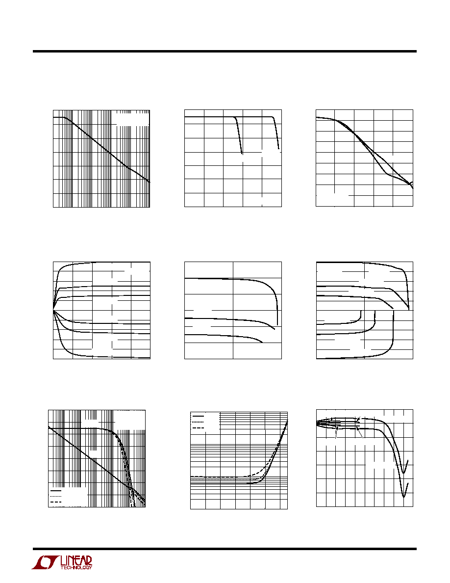
Bias Current vs Temperature
Single Supply Output Swing vs
Output Current
C
C
HARA TERISTICS
U
W
A
TYPICAL PERFOR
CE
Common Mode Rejection Ratio
vs Frequency
DC CMRR vs Common Mode Input
Voltage
Output Voltage Swing vs Load
Resistance
FREQUENCY (Hz)
20
CMRR (dB)
40
80
120
140
1
100
1k
100k
2054 G01
0
10
10k
60
100
V
S
= 3V OR 5V
V
CM
= 0.5V
P-P
V
CM
(V)
20
CMRR (dB)
40
80
120
140
1
3
4
0
2054 G02
0
2
5
60
100
V
S
= 3V
V
S
= 5V
T
A
= 25
∞
C
LOAD RESISTANCE (k
)
0
OUTPUT SWING (V)
2
4
2054 G03
6
8
10
5
4
3
2
1
0
≠1
≠ 2
≠ 3
≠ 4
≠ 5
R
L
TO GND
V
S
=
±
5V
V
S
=
±
2.5V
V
S
=
±
2.5V
V
S
=
±
1.5V
V
S
=
±
1.5V
V
S
=
±
5V
TEMPERATURE (
∞
C)
≠25
≠5
0.1
100
10
1
75
2054 G06
≠45
BIAS CURRENT (pA)
55
35
15
±
1.5V
±
2.5V
±
5V
FREQUENCY (Hz)
10
PSRR (dB)
140
120
100
80
60
40
20
0
≠20
≠40
100
1k
10k
100k
LTC2054 ∑ G14
1M
+PSRR
V
S
=
±
2.5V
V
IN
= 0.5V
RMS
≠PSRR
PSRR vs Frequency
INPUT COMMON MODE VOLTAGE (V)
INPUT BIAS CURRENT MAGNITUDE (pA)
8
10
2054 G13
6
5
7
9
2
0
4
3
1
4
0
≠4
≠8
≠12
≠16
≠20
≠24
IN
≠
, V
S
= 10V
IN
+
, V
S
= 10V
IN
≠
, V
S
= 5V
IN
+
, V
S
= 5V
IN
+
, V
S
= 3V
IN
≠
, V
S
= 3V
Input Bias Current vs Input
Common Mode Voltage
10
100
1k
10k
100k
1M
10M
FREQUENCY (Hz)
GAIN (dB)
20
40
60
120
100
2054 G05
≠20
≠40
80
≠160
≠140
≠120
≠60
≠80
≠200
0
≠180
≠220
≠100
PHASE (DEG)
V
S
=
±
2.5V
V
IN
= 0.5V
P-P
R
L
= 10k
C
L
= 30pF
C
L
= 50pF
C
L
= 100pF
GAIN
PHASE
Gain/Phase vs Frequency
Dual Supply Output Swing vs
Output Current