Äîêóìåíòàöèÿ è îïèñàíèÿ www.docs.chipfind.ru

LTC2230/LTC2231
1
22301p
Wireless and Wired Broadband Communication
Cable Head-End Systems
Power Amplifier Linearization
Communications Test Equipment
FEATURES
DESCRIPTIO
U
APPLICATIO S
U
TYPICAL APPLICATIO
U
Sample Rate: 170Msps/135 Msps
61dB SNR up to 140MHz Input
75dB SFDR up to 200MHz Input
775MHz Full Power Bandwidth S/H
Single 3.3V Supply
Low Power Dissipation: 890mW/660mW
LVDS, CMOS, or Demultiplexed CMOS Outputs
Selectable Input Ranges: ±0.5V or ±1V
No Missing Codes
Optional Clock Duty Cycle Stabilizer
Shutdown and Nap Modes
Data Ready Output Clock
Pin Compatible Family
170Msps: LTC2220 (12-Bit), LTC2230 (10-Bit)
135Msps: LTC2221 (12-Bit), LTC2231 (10-Bit)
64-Pin 9mm x 9mmQFN Package
10-Bit,170Msps/
135Msps ADCs
The LTC
®
2230 and LTC2231 are 170Msps/135Msps, sam-
pling 10-bit A/D converters designed for digitizing high
frequency, wide dynamic range signals. The LTC2230/
LTC2231 are perfect for demanding communications
applications with AC performance that includes 61dB SNR
and 75dB spurious free dynamic range for signals
up to 200MHz. Ultralow jitter of 0.15ps
RMS
allows
undersampling of IF frequencies with excellent noise
performance.
DC specs include ±0.2LSB INL (typ), ±0.1LSB DNL (typ)
and no missing codes over temperature. The transition
noise is a low 0.12LSB
RMS
.
The digital outputs can be either differential LVDS, or
single-ended CMOS. There are three format options for
the CMOS outputs: a single bus running at the full data rate
or two demultiplexed buses running at half data rate with
either interleaved or simultaneous update. A separate
output power supply allows the CMOS output swing to
range from 0.5V to 3.3V.
The ENC
+
and ENC
inputs may be driven differentially or
single ended with a sine wave, PECL, LVDS, TTL, or CMOS
inputs. An optional clock duty cycle stabilizer allows high
performance at full speed for a wide range of clock duty
cycles.
, LTC and LT are registered trademarks of Linear Technology Corporation.
+
INPUT
S/H
CORRECTION
LOGIC
OUTPUT
DRIVERS
10-BIT
PIPELINED
ADC CORE
CLOCK/DUTY
CYCLE
CONTROL
FLEXIBLE
REFERENCE
D9
·
·
·
D0
ENCODE INPUT
REFH
REFL
ANALOG
INPUT
22301 TA01
CMOS
OR
LVDS
3.3V
V
DD
OV
DD
OGND
0.5V
TO 3.3V
INPUT FREQUENCY (MHz)
0
SFDR (dBFS)
90
85
80
75
70
65
60
55
50
45
40
600
100
400
200
2230 TA01b
500
300
4th OR HIGHER
2nd OR 3rd
SFDR vs Input Frequency
Electrical Specifications Subject to Change
LTC2230/LTC2231
2
22301p
CO VERTER CHARACTERISTICS
U
Supply Voltage (V
DD
) ................................................. 4V
Digital Output Ground Voltage (OGND) ....... 0.3V to 1V
Analog Input Voltage (Note 3) ..... 0.3V to (V
DD
+ 0.3V)
Digital Input Voltage .................... 0.3V to (V
DD
+ 0.3V)
Digital Output Voltage ............... 0.3V to (OV
DD
+ 0.3V)
Power Dissipation ............................................ 1500mW
Operating Temperature Range
LTC2230C, LTC2231C ............................. 0°C to 70°C
LTC2230I, LTC2231I ...........................40°C to 85°C
Storage Temperature Range ..................65°C to 125°C
ORDER PART
NUMBER
UP PART
MARKING
T
JMAX
= 125°C,
JA
= 20°C/W
2230
2230
2231
2231
LTC2230CUP
LTC2230IUP
LTC2231CUP
LTC2231IUP
ABSOLUTE AXI U
RATI GS
W
W
W
U
PACKAGE/ORDER I FOR ATIO
U
U
W
OV
DD
= V
DD
(Notes 1, 2)
The
denotes the specifications which apply over the full operating
temperature range, otherwise specifications are at T
A
= 25°C. (Note 4)
PARAMETER
CONDITIONS
MIN
TYP
MAX
UNITS
Resolution (No Missing Codes)
10
Bits
Integral Linearity Error
Differential Analog Input
0.8
±0.2
0.8
LSB
Differential Linearity Error
Differential Analog Input
0.6
±0.1
0.6
LSB
Integral Linearity Error
Single-Ended Analog Input
±0.5
LSB
Differential Linearity Error
Single-Ended Analog Input
±0.1
LSB
Offset Error
20
±3
20
mV
Gain Error
External Reference
3
±0.5
3
%FS
Offset Drift
±10
µV/C
Full-Scale Drift
Internal Reference
±30
ppm/C
External Reference
±15
ppm/C
Transition Noise
SENSE = 1V
0.12
LSB
RMS
Consult LTC Marketing for parts specified with wider operating temperature ranges.
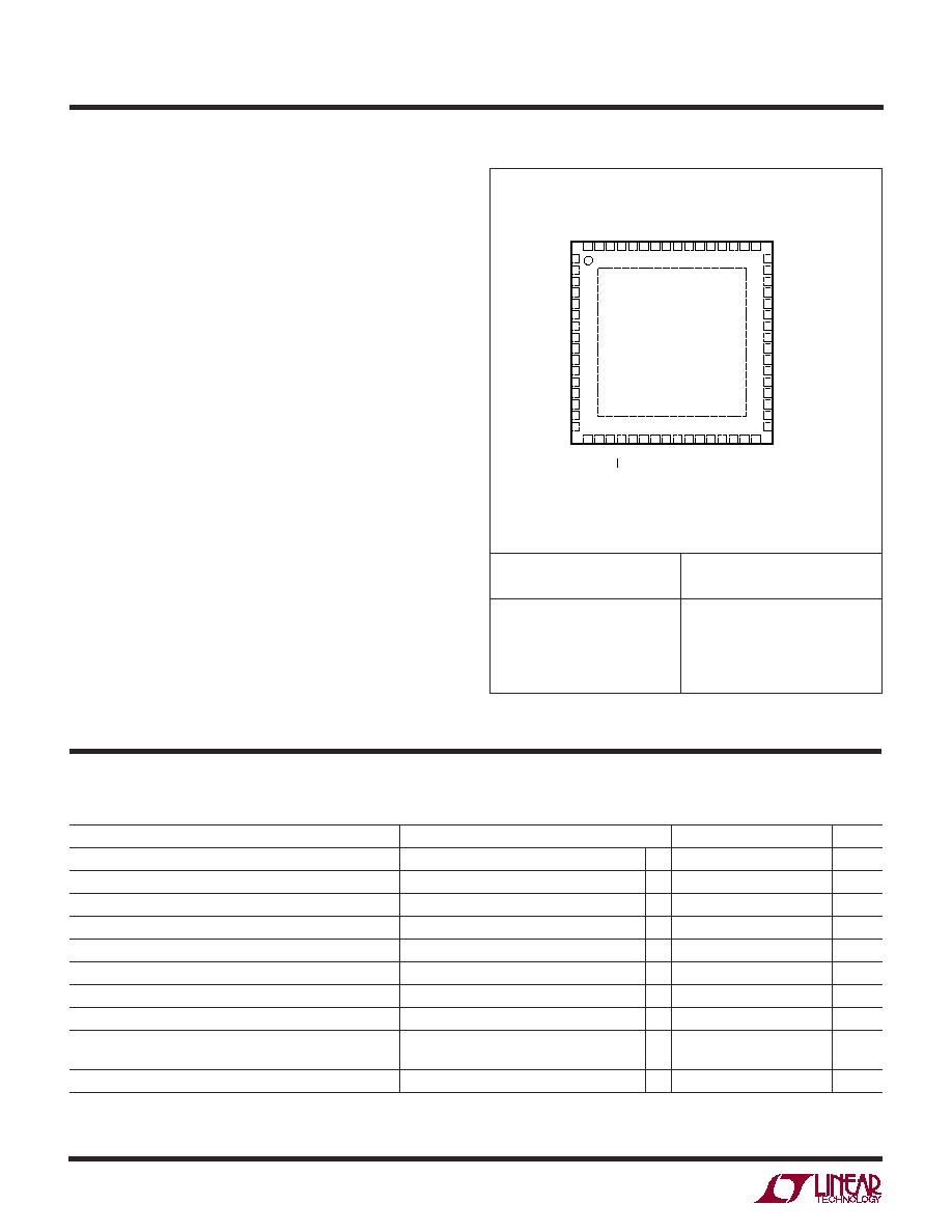
TOP VIEW
UP PACKAGE
64-LEAD (9mm × 9mm) PLASTIC QFN
EXPOSED PAD IS GND (PIN 65),
MUST BE SOLDERED TO PCB
A
IN
+
1
A
IN
+
2
A
IN
3
A
IN
4
REFHA 5
REFHA 6
REFLB
7
REFLB
8
REFHB 9
REFHB 10
REFLA 11
REFLA 12
V
DD
13
V
DD
14
V
DD
15
GND 16
48 D7
+
/DA4
47 D7
/DA3
46 D6
+
/DA2
45 D6
/DA1
44 D5
+
/DA0
43 D5
/DNC
42 OV
DD
41 OGND
40 D4
+
/DNC
39 D4
/CLOCKOUTA
38 D3
+
/CLOCKOUTB
37 D3
/OFB
36 CLOCKOUT
+
/DB9
35 CLOCKOUT
/DB8
34 OV
DD
33 OGND
64 GND
63 V
DD
62 V
DD
61 GND
60 V
CM
59 SENSE
58 MODE
57 LVDS
56 OF
+
/OFA
55 OF
/DA9
54 D9
+
/DA8
53 D9
/DA7
52 D8
+
/DA6
51 D8
/DA5
50 OGND
49 OV
DD
ENC
+
17
ENC
18
SHDN
19
OE
20
DNC 21
DNC 22
DNC/DB0 23
DNC/DB1 24
OGND 25
OV
DD
26
D0
/DB2 27
D0
+
/DB3 28
D1
/DB4 29
D1
+
/DB5 30
D2
/DB6 31
D2
+
/DB7 32
65
LTC2230/LTC2231
3
22301p
SYMBOL
PARAMETER
CONDITIONS
MIN
TYP
MAX
UNITS
V
IN
Analog Input Range (A
IN
+
A
IN
)
3.1V < V
DD
< 3.5V
±0.5 to ±1
V
V
IN, CM
Analog Input Common Mode
Differential Input
1
1.6
1.9
V
I
IN
Analog Input Leakage Current
0 < A
IN
+
, A
IN
< V
DD
1
1
µA
I
SENSE
SENSE Input Leakage
0V < SENSE < 1V
1
1
µA
I
MODE
MODE Pin Pull-Down Current to GND
10
µA
I
LVDS
LVDS Pin Pull-Down Current to GND
10
µA
t
AP
Sample and Hold Acquisition Delay Time
0
ns
t
JITTER
Sample and Hold Acquisition Delay Time Jitter
0.15
ps
RMS
CMRR
Analog Input Common Mode Rejection Ratio
80
dB
Full Power Bandwidth
Figure 8 Test Circuit
775
MHz
LTC2230
LTC2231
SYMBOL
PARAMETER
CONDITIONS
MIN
TYP
MAX
MIN
TYP
MAX
UNITS
SNR
Signal-to-Noise Ratio (Note 10)
5MHz Input (1V Range)
59.5
59.5
dB
5MHz Input (2V Range)
61.2
61.2
dB
70MHz Input (1V Range)
59.5
59.5
dB
70MHz Input (2V Range)
60
61.1
60
61.1
dB
140MHz Input (1V Range)
59.4
59.4
dB
140MHz Input (2V Range)
61.0
61.0
dB
250MHz Input (1V Range)
59.0
59.0
dB
250MHz Input (2V Range)
60.6
60.6
dB
SFDR
Spurious Free Dynamic Range
5MHz Input (1V Range)
80
80
dB
2nd or 3rd Harmonic (Note 11)
5MHz Input (2V Range)
78
78
dB
70MHz Input (1V Range)
80
80
dB
70MHz Input (2V Range)
70
78
70
78
dB
140MHz Input (1V Range)
78
78
dB
140MHz Input (2V Range)
78
78
db
250MHz Input (1V Range)
75
78
dB
250MHz Input (2V Range)
74
78
dB
SFDR
Spurious Free Dynamic Range
5MHz Input (1V Range)
86
86
dB
4th Harmonic or Higher (Note 11)
5MHz Input (2V Range)
86
86
dB
70MHz Input (1V Range)
86
86
dB
70MHz Input (2V Range)
75
86
75
86
dB
140MHz Input (1V Range)
86
86
dB
140MHz Input (2V Range)
86
86
dB
250MHz Input (1V Range)
85
85
dB
250MHz Input (2V Range)
85
85
dB
S/(N+D)
Signal-to-Noise
5MHz Input (1V Range)
59.5
59.5
dB
Plus Distortion Ratio (Note 12)
5MHz Input (2V Range)
61.2
61.2
dB
70MHz Input (1V Range)
59.5
59.5
dB
70MHz Input (2V Range)
60
61.1
60
61.1
dB
IMD
Intermodulation Distortion
f
IN1
= 138MHz,
81
81
dBc
f
IN2
= 140MHz
A ALOG I PUT
U
U
DY
A
IC ACCURACY
U
W
The
denotes the specifications which apply over the full operating temperature range, otherwise
specifications are at T
A
= 25°C. (Note 9)
T
A
= 25°C. A
IN
= 1dBFS. (Note 4)
LTC2230/LTC2231
4
22301p
DIGITAL I PUTS A D DIGITAL OUTPUTS
U
U
The
denotes the specifications which apply over the
full operating temperature range, otherwise specifications are at T
A
= 25°C. (Note 4)
I TER AL REFERE CE CHARACTERISTICS
U
U
U
(Note 4)
PARAMETER
CONDITIONS
MIN
TYP
MAX
UNITS
V
CM
Output Voltage
I
OUT
= 0
1.575
1.600
1.625
V
V
CM
Output Tempco
±25
ppm/C
V
CM
Line Regulation
3.1V < V
DD
< 3.5V
3
mV/V
V
CM
Output Resistance
1mA < I
OUT
< 1mA
4
SYMBOL
PARAMETER
CONDITIONS
MIN
TYP
MAX
UNITS
ENCODE INPUTS (ENC
+
, ENC
)
V
ID
Differential Input Voltage
0.2
V
V
ICM
Common Mode Input Voltage
Internally Set
1.6
V
Externally Set (Note 7)
1.1
1.6
2.5
V
R
IN
Input Resistance
6
k
C
IN
Input Capacitance
(Note 7)
3
pF
LOGIC INPUTS (OE, SHDN)
V
IH
High Level Input Voltage
V
DD
= 3.3V
2
V
V
IL
Low Level Input Voltage
V
DD
= 3.3V
0.8
V
I
IN
Input Current
V
IN
= 0V to V
DD
10
10
µA
C
IN
Input Capacitance
(Note 7)
3
pF
LOGIC OUTPUTS (CMOS MODE)
OV
DD
= 3.3V
C
OZ
Hi-Z Output Capacitance
OE = High (Note 7)
3
pF
I
SOURCE
Output Source Current
V
OUT
= 0V
50
mA
I
SINK
Output Sink Current
V
OUT
= 3.3V
50
mA
V
OH
High Level Output Voltage
I
O
= 10µA
3.295
V
I
O
= 200µA
3.1
3.29
V
V
OL
Low Level Output Voltage
I
O
= 10µA
0.005
V
I
O
= 1.6mA
0.09
0.4
V
OV
DD
= 2.5V
V
OH
High Level Output Voltage
I
O
= 200µA
2.49
V
V
OL
Low Level Output Voltage
I
O
= 1.6mA
0.09
V
OV
DD
= 1.8V
V
OH
High Level Output Voltage
I
O
= 200µA
1.79
V
V
OL
Low Level Output Voltage
I
O
= 1.6mA
0.09
V
LOGIC OUTPUTS (LVDS MODE)
V
OD
Differential Output Voltage
100 Differential Load
247
350
454
mV
V
OS
Output Common Mode Voltage
100 Differential Load
1.125
1.250
1.375
V
LTC2230/LTC2231
5
22301p
POWER REQUIRE E TS
W
U
TI I G CHARACTERISTICS
U
W
The
denotes the specifications which apply over the full operating temperature
range, otherwise specifications are at T
A
= 25°C. (Note 4)
LTC2230
LTC2231
SYMBOL
PARAMETER
CONDITIONS
MIN
TYP
MAX
MIN
TYP
MAX
UNITS
V
DD
Analog Supply Voltage
3.1
3.3
3.5
3.1
3.3
3.5
V
P
SHDN
Shutdown Power
SHDN = H, OE = H, No CLK
2
2
mW
P
NAP
Nap Mode Power
SHDN = H, OE = L, No CLK
35
35
mW
LVDS OUTPUT MODE
OV
DD
Output Supply Voltage
3
3.3
3.6
3
3.3
3.6
V
I
VDD
Analog Supply Current
264
290
196
216
mA
I
OVDD
Output Supply Current
55
61
55
61
mA
P
DISS
Power Dissipation
1050
1160
828
915
mW
CMOS OUTPUT MODE
OV
DD
Output Supply Voltage
0.5
3.3
3.6
0.5
3.3
3.6
V
I
VDD
Analog Supply Current
264
290
196
216
mA
P
DISS
Power Dissipation
890
660
mW
LTC2230
LTC2231
SYMBOL
PARAMETER
CONDITIONS
MIN
TYP
MAX
MIN
TYP
MAX
UNITS
f
S
Sampling Frequency
1
170
1
135
MHz
t
L
ENC Low Time
Duty Cycle Stabilizer Off
2.8
2.94
500
3.5
3.7
500
ns
Duty Cycle Stabilizer On
2
2.94
500
2
3.7
500
ns
t
H
ENC High Time
Duty Cycle Stabilizer Off
2.8
2.94
500
3.5
3.7
500
ns
Duty Cycle Stabilizer On
2
2.94
500
2
3.7
500
ns
t
AP
Sample-and-Hold Aperture Delay
0
0
ns
t
OE
Output Enable Delay
(Note 7)
5
10
5
10
ns
LVDS OUTPUT MODE
t
D
ENC to DATA Delay
(Note 7)
1.3
2.2
3.5
1.3
2.2
3.5
ns
t
C
ENC to CLOCKOUT Delay
(Note 7)
1.3
2.2
3.5
1.3
2.2
3.5
ns
DATA to CLOCKOUT Skew
(t
C
- t
D
) (Note 7)
0.6
0
0.6
0.6
0
0.6
ns
Rise Time
0.5
0.5
ns
Fall Time
0.5
0.5
ns
Pipeline Latency
5
5
Cycles
CMOS OUTPUT MODE
t
D
ENC to DATA Delay
(Note 7)
1.3
2.1
3.5
1.3
2.1
3.5
ns
t
C
ENC to CLOCKOUT Delay
(Note 7)
1.3
2.1
3.5
1.3
2.1
3.5
ns
DATA to CLOCKOUT Skew
(t
C
- t
D
) (Note 7)
0.6
0
0.6
0.6
0
0.6
ns
Pipeline Latency Full Rate CMOS
5
5
Cycles
Demuxed Interleaved
5
5
Cycles
Demuxed Simultaneous
5 and 6
5 and 6
Cycles
The
denotes the specifications which apply over the full operating temperature
range, otherwise specifications are at T
A
= 25°C. (Note 9)