1
LTC2421/LTC2422
24212f
1-/2-Channel 20-Bit
µ
Power
No Latency
TM
ADCs in MSOP-10
s
Weight Scales
s
Direct Temperature Measurement
s
Gas Analyzers
s
Strain Gauge Transducers
s
Instrumentation
s
Data Acquisition
s
Industrial Process Control
No Latency
is a trademark of Linear Technology Corporation.
MICROWIRE is a trademark of National Semiconductor Corporation.
Pseudo Differential Bridge Digitizer
, LTC and LT are registered trademarks of Linear Technology Corporation.
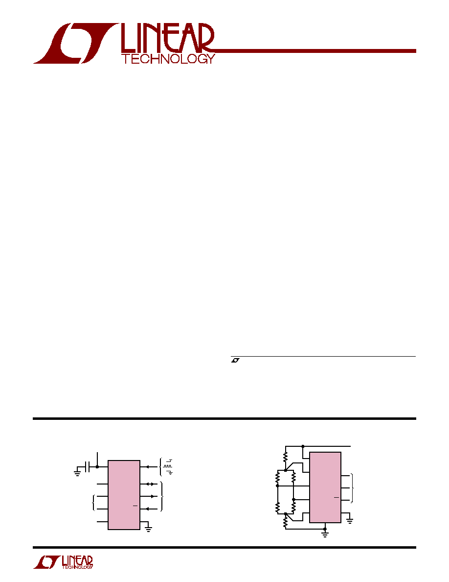
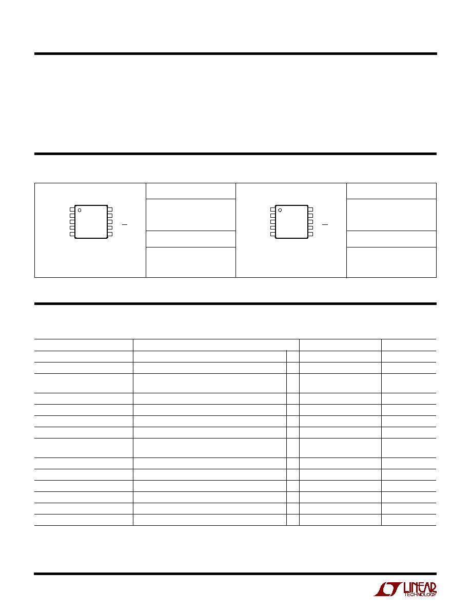
The LTC
Æ
2421/LTC2422 are 1- and 2-channel 2.7V to 5.5V
micropower 20-bit analog-to-digital converters with an
integrated oscillator, 8ppm INL and 1.2ppm RMS noise.
These ultrasmall devices use delta-sigma technology and
a new digital filter architecture that settles in a single cycle.
This eliminates the latency found in conventional
converters and simplifies multiplexed applications.
Through a single pin, the LTC2421/LTC2422 can be
configured for better than 110dB rejection at 50Hz or
60Hz
±
2%, or can be driven by an external oscillator for
a user defined rejection frequency in the range 1Hz to
120Hz. The internal oscillator requires no external fre-
quency setting components.
These converters accept an external reference voltage
from 0.1V to V
CC
. With an extended input conversion
range of ≠12.5% V
REF
to 112.5% V
REF
(V
REF
= FS
SET
≠
ZS
SET
), the LTC2421/LTC2422 smoothly resolve the off-
set and overrange problems of preceding sensors or
signal conditioning circuits.
The LTC2421/LTC2422 communicate through a 2- or
3-wire digital interface that is compatible with SPI and
MICROWIRE
TM
protocols.
s
20-Bit ADCs in Tiny MSOP-10 Packages
s
1- or 2-Channel Inputs
s
Single Supply 2.7V to 5.5V Operation
s
Low Supply Current (200
µ
A) and Auto Shutdown
s
Automatic Channel Selection (Ping-Pong) (LTC2422)
s
No Latency: Digital Filter Settles in a
Single Conversion Cycle
s
8ppm INL, No Missing Codes
s
4ppm Full-Scale Error
s
0.5ppm Offset
s
1.2ppm Noise
s
Zero Scale and Full Scale Set for Reference
and Ground Sensing
s
Internal Oscillator--No External Components Required
s
110dB Min, 50Hz/60Hz Notch Filter
s
Reference Input Voltage: 0.1V to V
CC
s
Live Zero--Extended Input Range Accommodates
12.5% Overrange and Underrange
s
Pin Compatible with LTC2401/LTC2402
ANALOG INPUT RANGE
ZS
SET
≠ 0.12V
REF
TO
FS
SET
+ 0.12V
REF
(V
REF
= FS
SET
≠ ZS
SET
)
V
CC
F
O
FS
SET
ZS
SET
SCK
CH1
SDO
GND
CS
REFERENCE VOLTAGE
ZS
SET
+ 0.1V TO V
CC
0V TO FS
SET
≠ 100mV
CH0
= INTERNAL OSC/50Hz REJECTION
= EXTERNAL CLOCK SOURCE
= INTERNAL OSC/60Hz REJECTION
3-WIRE
SPI INTERFACE
1
µ
F
1
10
9
8
7
6
2
3
4
5
2.7V TO 5.5V
LTC2422
24212 TA01
V
CC
V
CC
FS
SET
ZS
SET
SCK
CH0
SDO
F
O
CS
CH1
GND
LTC2422
3-WIRE
SPI INTERFACE
INTERNAL OSCILLATOR
60Hz REJECTION
1
9
2.7V TO 5.5V
8
7
10
6
24012TA02
2
4
3
5
DESCRIPTIO
U
FEATURES
APPLICATIO S
U
TYPICAL APPLICATIO
U
2
LTC2421/LTC2422
24212f
ORDER PART NUMBER
(Notes 1, 2)
Supply Voltage (V
CC
) to GND .......................≠ 0.3V to 7V
Analog Input Voltage to GND ....... ≠ 0.3V to (V
CC
+ 0.3V)
Reference Input Voltage to GND .. ≠ 0.3V to (V
CC
+ 0.3V)
Digital Input Voltage to GND ........ ≠ 0.3V to (V
CC
+ 0.3V)
Digital Output Voltage to GND ..... ≠ 0.3V to (V
CC
+ 0.3V)
T
JMAX
= 125
∞
C,
JA
= 130
∞
C/W
LTC2421CMS
LTC2421IMS
ABSOLUTE
M
AXI
M
U
M
RATINGS
W
W
W
U
PACKAGE/ORDER I
N
FOR
M
ATIO
N
U
U
W
1
2
3
4
5
V
CC
FS
SET
CH1
CH0
ZS
SET
10
9
8
7
6
F
O
SCK
SDO
CS
GND
TOP VIEW
MS10 PACKAGE
10-LEAD PLASTIC MSOP
Operating Temperature Range
LTC2421/LTC2422C ................................ 0
∞
C to 70
∞
C
LTC2421/LTC2422I ............................ ≠ 40
∞
C to 85
∞
C
Storage Temperature Range ................. ≠ 65
∞
C to 150
∞
C
Lead Temperature (Soldering, 10 sec).................. 300
∞
C
ORDER PART NUMBER
MS10 PART MARKING
LTC2422CMS
LTC2422IMS
LTUZ
LTVA
MS10 PART MARKING
LTUX
LTUY
T
JMAX
= 125
∞
C,
JA
= 130
∞
C/W
PARAMETER
CONDITIONS
MIN
TYP
MAX
UNITS
Resolution
q
20
Bits
No Missing Codes Resolution
0.1V
FS
SET
V
CC
, ZS
SET
= 0V (Note 5)
q
20
Bits
Integral Nonlinearity
FS
SET
= 2.5V, ZS
SET
= 0V (Note 6)
q
4
10
ppm of V
REF
FS
SET
= 5V, ZS
SET
= 0V (Note 6)
q
8
20
ppm of V
REF
Offset Error
2.5V
FS
SET
V
CC
, ZS
SET
= 0V
q
0.5
10
ppm of V
REF
Offset Error Drift
2.5V
FS
SET
V
CC
, ZS
SET
= 0V
0.04
ppm of V
REF
/
∞
C
Full-Scale Error
2.5V
FS
SET
V
CC
, ZS
SET
= 0V
q
4
10
ppm of V
REF
Full-Scale Error Drift
2.5V
FS
SET
V
CC
, ZS
SET
= 0V
0.04
ppm of V
REF
/
∞
C
Total Unadjusted Error
FS
SET
= 2.5V, ZS
SET
= 0V
8
ppm of V
REF
FS
SET
= 5V, ZS
SET
= 0V
16
ppm of V
REF
Output Noise
V
IN
= 0V (Note 13)
6
µ
V
RMS
Normal Mode Rejection 60Hz
±
2%
(Note 7)
q
110
130
dB
Normal Mode Rejection 50Hz
±
2%
(Note 8)
q
110
130
dB
Power Supply Rejection, DC
FS
SET
= 2.5V, ZS
SET
= 0V, V
IN
= 0V
100
dB
Power Supply Rejection, 60Hz
±
2%
FS
SET
= 2.5V, ZS
SET
= 0V, V
IN
= 0V, (Notes 7, 15)
110
dB
Power Supply Rejection, 50Hz
±
2%
FS
SET
= 2.5V, ZS
SET
= 0V, V
IN
= 0V, (Notes 8, 15)
110
dB
The
q
denotes specifications which apply over the full operating
temperature range, otherwise specifications are at T
A
= 25
∞
C. V
REF
= FS
SET
≠ ZS
SET
. (Notes 3, 4)
CO
N
VERTER CHARACTERISTICS
U
1
2
3
4
5
V
CC
FS
SET
V
IN
NC
ZS
SET
10
9
8
7
6
TOP VIEW
MS10 PACKAGE
10-LEAD PLASTIC MSOP
F
O
SCK
SDO
CS
GND
Consult factory for parts specified with wider operating temperature ranges.
3
LTC2421/LTC2422
24212f
SYMBOL
PARAMETER
CONDITIONS
MIN
TYP
MAX
UNITS
V
IH
High Level Input Voltage
2.7V
V
CC
5.5V
q
2.5
V
CS, F
O
2.7V
V
CC
3.3V
2.0
V
V
IL
Low Level Input Voltage
4.5V
V
CC
5.5V
q
0.8
V
CS, F
O
2.7V
V
CC
5.5V
0.6
V
V
IH
High Level Input Voltage
2.7V
V
CC
5.5V (Note 9)
q
2.5
V
SCK
2.7V
V
CC
3.3V (Note 9)
2.0
V
V
IL
Low Level Input Voltage
4.5V
V
CC
5.5V (Note 9)
q
0.8
V
SCK
2.7V
V
CC
5.5V (Note 9)
0.6
V
I
IN
Digital Input Current
0V
V
IN
V
CC
q
≠10
10
µ
A
CS, F
O
I
IN
Digital Input Current
0V
V
IN
V
CC
(Note 9)
q
≠10
10
µ
A
SCK
C
IN
Digital Input Capacitance
10
pF
CS, F
O
C
IN
Digital Input Capacitance
(Note 9)
10
pF
SCK
V
OH
High Level Output Voltage
I
O
= ≠ 800
µ
A
q
V
CC
≠ 0.5
V
SDO
V
OL
Low Level Output Voltage
I
O
= 1.6mA
q
0.4
V
SDO
V
OH
High Level Output Voltage
I
O
= ≠ 800
µ
A (Note 10)
q
V
CC
≠ 0.5
V
SCK
V
OL
Low Level Output Voltage
I
O
= 1.6mA (Note 10)
q
0.4
V
SCK
I
OZ
High-Z Output Leakage
q
≠10
10
µ
A
SDO
DIGITAL I PUTS A D DIGITAL OUTPUTS
U
U
SYMBOL
PARAMETER
CONDITIONS
MIN
TYP
MAX
UNITS
V
CC
Supply Voltage
q
2.7
5.5
V
I
CC
Supply Current
Conversion Mode
CS = 0V (Note 12)
q
200
300
µ
A
Sleep Mode
CS = V
CC
(Note 12)
q
20
30
µ
A
POWER REQUIRE E TS
W
U
The
q
denotes specifications which apply over the full
operating temperature range, otherwise specifications are at T
A
= 25
∞
C. (Note 3)
The
q
denotes specifications which apply over the full operating temperature range,
otherwise specifications are at T
A
= 25
∞
C. (Note 3)
SYMBOL
PARAMETER
CONDITIONS
MIN
TYP
MAX
UNITS
V
IN
Input Voltage Range
(Note 14)
q
ZS
SET
≠ 0.12V
REF
FS
SET
+ 0.12V
REF
V
FS
SET
Full-Scale Set Range
q
0.1 + ZS
SET
V
CC
V
ZS
SET
Zero-Scale Set Range
q
0
FS
SET
≠ 0.1
V
C
S(IN)
Input Sampling Capacitance
1
pF
C
S(REF)
Reference Sampling Capacitance
1.5
pF
I
IN(LEAK)
Input Leakage Current
CS = V
CC
q
≠100
1
100
nA
I
REF(LEAK)
Reference Leakage Current
V
REF
= 2.5V, CS = V
CC
q
≠ 100
1
100
nA
The
q
denotes specifications which apply over the full operating
temperature range, otherwise specifications are at T
A
= 25
∞
C. V
REF
= FS
SET
≠ ZS
SET
. (Note 3)
A ALOG I PUT A D REFERE CE
U
U
U
U
4
LTC2421/LTC2422
24212f
The
q
denotes specifications which apply over the full operating temperature
range, otherwise specifications are at T
A
= 25
∞
C. (Note 3)
f
EOSC
External Oscillator Frequency Range
q
2.56
307.2
kHz
t
HEO
External Oscillator High Period
q
0.5
390
µ
s
t
LEO
External Oscillator Low Period
q
0.5
390
µ
s
t
CONV
Conversion Time
F
O
= 0V
q
130.86
133.53
136.20
ms
F
O
= V
CC
q
157.03
160.23
163.44
ms
External Oscillator (Note 11)
q
20510/f
EOSC
(in kHz)
ms
f
ISCK
Internal SCK Frequency
Internal Oscillator (Note 10)
19.2
kHz
External Oscillator (Notes 10, 11)
f
EOSC
/8
kHz
D
ISCK
Internal SCK Duty Cycle
(Note 10)
45
55
%
f
ESCK
External SCK Frequency Range
(Note 9)
q
2000
kHz
t
LESCK
External SCK Low Period
(Note 9)
q
250
ns
t
HESCK
External SCK High Period
(Note 9)
q
250
ns
t
DOUT_ISCK
Internal SCK 24-Bit Data Output Time
Internal Oscillator (Notes 10, 12)
q
1.23
1.25
1.28
ms
External Oscillator (Notes 10, 11)
q
192/f
EOSC
(in kHz)
ms
t
DOUT_ESCK
External SCK 24-Bit Data Output Time
(Note 9)
q
24/f
ESCK
(in kHz)
ms
t
1
CS
to SDO Low Z
q
0
150
ns
t
2
CS
to SDO High Z
q
0
150
ns
t
3
CS
to SCK
(Note 10)
q
0
150
ns
t
4
CS
to SCK
(Note 9)
q
50
ns
t
KQMAX
SCK
to SDO Valid
q
200
ns
t
KQMIN
SDO Hold After SCK
(Note 5)
q
15
ns
t
5
SCK Set-Up Before CS
q
50
ns
t
6
SCK Hold After CS
q
50
ns
SYMBOL
PARAMETER
CONDITIONS
MIN
TYP
MAX
UNITS
Note 1: Absolute Maximum Ratings are those values beyond which the
life of the device may be impaired.
Note 2: All voltage values are with respect to GND.
Note 3: V
CC
= 2.7 to 5.5V unless otherwise specified. Input source
resistance = 0
.
Note 4: Internal Conversion Clock source with the F
O
pin tied
to GND or to V
CC
or to external conversion clock source with
f
EOSC
= 153600Hz unless otherwise specified.
Note 5: Guaranteed by design, not subject to test.
Note 6: Integral nonlinearity is defined as the deviation of a code from
a straight line passing through the actual endpoints of the transfer
curve. The deviation is measured from the center of the quantization
band.
Note 7: F
O
= 0V (internal oscillator) or f
EOSC
= 153600Hz
±
2%
(external oscillator).
Note 8: F
O
= V
CC
(internal oscillator) or f
EOSC
= 128000Hz
±
2%
(external oscillator).
Note 9: The converter is in external SCK mode of operation such that
the SCK pin is used as digital input. The frequency of the clock signal
driving SCK during the data output is f
ESCK
and is expressed in kHz.
Note 10: The converter is in internal SCK mode of operation such that
the SCK pin is used as digital output. In this mode of operation, the
SCK pin has a total equivalent load capacitance C
LOAD
= 20pF.
Note 11: The external oscillator is connected to the F
O
pin. The external
oscillator frequency, f
EOSC
, is expressed in kHz.
Note 12: The converter uses the internal oscillator.
F
O
= 0V or F
O
= V
CC
.
Note 13: The output noise includes the contribution of the internal
calibration operations.
Note 14: V
REF
= FS
SET
≠ ZS
SET
. The minimum input voltage is limited
to ≠ 0.3V and the maximum to V
CC
+ 0.3V.
Note 15: V
CC
(DC) = 4.1V, V
CC
(AC) = 2.8V
P-P
.
TI I G CHARACTERISTICS
U
W
5
LTC2421/LTC2422
24212f
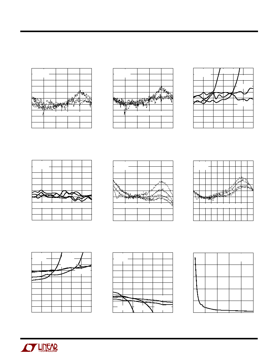
TYPICAL PERFOR A CE CHARACTERISTICS
U
W
Total Unadjusted Error (3V Supply)
INL (3V Supply)
Negative Extended Input Range
Total Unadjusted Error (3V Supply)
Positive Extended Input Range
Total Unadjusted Error (3V Supply)
Total Unadjusted Error (5V Supply)
INL (5V Supply)
Negative Extended Input Range
Total Unadjusted Error (5V Supply)
Offset Error vs Reference Voltage
Positive Extended Input Range
Total Unadjusted Error (5V Supply)
INPUT VOLTAGE (V)
0
ERROR (ppm)
2
6
10
2.0
24212 G01
≠2
≠6
0
4
8
≠4
≠8
≠10
0.5
1.0
1.5
2.5
V
CC
= 3V
V
REF
= 2.5V
T
A
= ≠55
∞
C, ≠45
∞
C, 25
∞
C, 90
∞
C
INPUT VOLTAGE (V)
0
ERROR (ppm)
2
6
10
2.0
24212 G02
≠2
≠6
0
4
8
≠4
≠8
≠10
0.5
1.0
1.5
2.5
V
CC
= 3V
V
REF
= 2.5V
T
A
= ≠55
∞
C, ≠45
∞
C, 25
∞
C, 90
∞
C
INPUT VOLTAGE (V)
0
≠10
≠6
≠2
2
≠0.05 ≠0.10 ≠0.15 ≠0.20
24212 G03
≠0.25
10
≠0.30
ERROR (ppm)
6
≠8
≠4
0
8
4
V
CC
= 3V
V
REF
= 2.5V
T
A
= 90
∞
C
T
A
= 25
∞
C
T
A
= ≠45
∞
C
T
A
= ≠55
∞
C
INPUT VOLTAGE (V)
2.50
≠10
≠6
≠2
2
2.55
2.60
2.65
2.70
24212 G04
2.75
10
2.80
ERROR (ppm)
6
≠8
≠4
0
8
4
V
CC
= 3V
V
REF
= 2.5V
T
A
= ≠55
∞
C, ≠45
∞
C, 25
∞
C, 90
∞
C
INPUT VOLTAGE (V)
0
ERROR (ppm)
2
6
10
4
24212 G05
≠2
≠6
0
4
8
≠4
≠8
≠10
1
2
3
5
V
CC
= 5V
V
REF
= 5V
T
A
= ≠55
∞
C, ≠45
∞
C, 25
∞
C, 90
∞
C
INPUT VOLTAGE (V)
0
ERROR (ppm)
2
6
10
4
24212 G06
≠2
≠6
0
4
8
≠4
≠8
≠10
1
2
3
5
V
CC
= 5V
V
REF
= 5V
T
A
= ≠55
∞
C, ≠45
∞
C, 25
∞
C, 90
∞
C
INPUT VOLTAGE (V)
0
≠10
≠6
≠2
2
≠0.05 ≠0.10 ≠0.15 ≠0.20
24212 G07
≠0.25
10
≠0.30
ERROR (ppm)
6
≠8
≠4
0
8
4
V
CC
= 5V
V
REF
= 5V
T
A
= 90
∞
C
T
A
= 25
∞
C
T
A
= ≠55
∞
C
T
A
= ≠45
∞
C
INPUT VOLTAGE (V)
5.00
≠10
≠6
≠2
2
5.05
5.10
5.15
5.20
24212 G08
5.25
10
5.30
ERROR (ppm)
6
≠8
≠4
0
8
4
V
CC
= 5V
V
REF
= 5V
T
A
= ≠45
∞
C
T
A
= ≠55
∞
C
T
A
= 25
∞
C
T
A
= 90
∞
C
REFERENCE VOLTAGE (V)
0
OFFSET ERROR (ppm)
90
120
150
4
24212 G09
60
30
0
1
2
3
5
V
CC
= 5V
T
A
= 25
∞
C
6
LTC2421/LTC2422
24212f
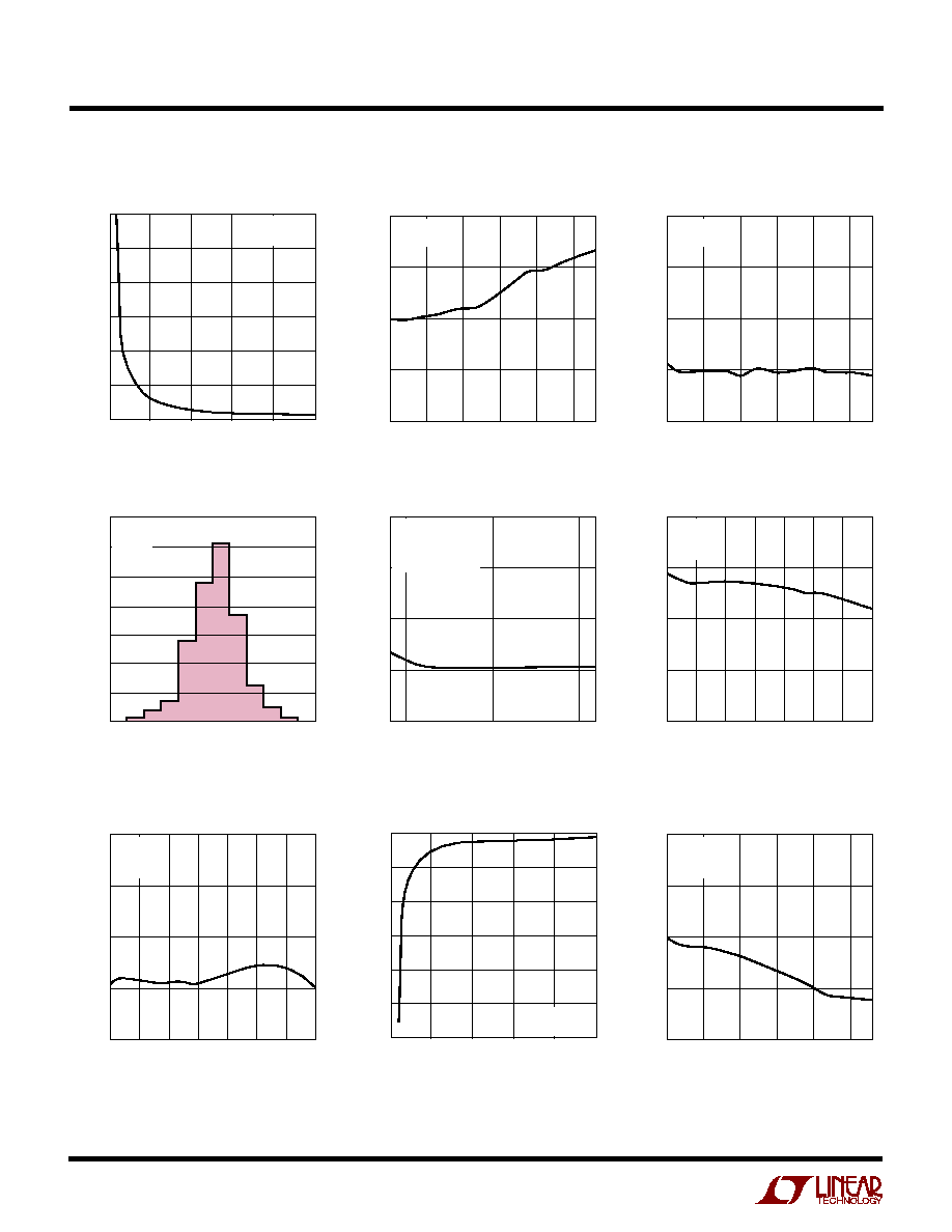
TYPICAL PERFOR A CE CHARACTERISTICS
U
W
RMS Noise vs Reference Voltage
Offset Error vs V
CC
RMS Noise vs V
CC
Noise Histogram
RMS Noise vs Code Out
Offset Error vs Temperature
Full-Scale Error vs Temperature
Full-Scale Error
vs Reference Voltage
Full-Scale Error vs V
CC
REFERENCE VOLTAGE (V)
0
0
RMS NOISE (ppm OF V
REF
)
10
20
30
40
50
60
1
2
3
4
24212 G10
5
V
CC
= 5V
T
A
= 25
∞
C
V
CC
(V)
2.7
≠10
OFFSET ERROR (ppm)
≠5
0
5
10
3.2
3.7
4.2
4.7
24212 G11
5.2 5.5
V
REF
= 2.5V
T
A
= 25
∞
C
V
CC
(V)
2.7
0
RMS NOISE (ppm)
2.5
5.0
7.5
10.0
3.2
3.7
4.2
4.7
24212 G12
5.2 5.5
V
REF
= 2.5V
T
A
= 25
∞
C
OUTPUT CODE (ppm)
0
50
100
150
200
250
300
350
2
6
24212 G13
≠2
0
4
NUMBER OF READINGS
V
CC
= 5
V
REF
= 5
V
IN
= 0
CODE OUT (HEX)
0
7FFFF
FFFFF
0
RMS NOISE (ppm)
1.25
2.50
3.75
5.00
24212 G14
V
CC
= 5V
V
REF
= 5V
V
IN
= 0.3V TO 5.3V
T
A
= 25
∞
C
TEMPERATURE (
∞
C)
≠55
≠10
OFFSET ERROR (ppm)
≠5
0
5
10
≠30
≠5
20
45
24212 G15
70
95
120
V
CC
= 5V
V
REF
= 5V
V
IN
= 0V
TEMPERATURE (
∞
C)
≠55
≠10
FULL-SCALE ERROR (ppm)
≠5
0
5
10
≠30
≠5
20
45
24212 G16
70
95
120
V
CC
= 5V
V
REF
= 5V
V
IN
= 5V
REFERENCE VOLTAGE (V)
0
≠150
FULL-SCALE ERROR (ppm)
≠125
≠100
≠75
≠50
≠25
0
1
2
3
4
24212 G17
5
V
CC
= 5V
V
IN
= V
REF
V
CC
(V)
2.7
≠10
FULL-SCALE ERROR (ppm)
≠5
0
5
10
3.2
3.7
4.2
4.7
24212 G18
5.2 5.5
V
REF
= 2.5V
V
IN
= 2.5V
T
A
= 25
∞
C
7
LTC2421/LTC2422
24212f
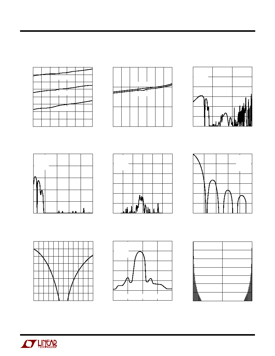
TYPICAL PERFOR A CE CHARACTERISTICS
U
W
Conversion Current
vs Temperature
Sleep Current vs Temperature
Rejection vs Frequency at V
IN
Rejection vs Frequency at V
IN
Rejection vs Frequency at V
IN
Rejection vs Frequency at V
IN
Rejection vs Frequency at V
CC
Rejection vs Frequency at V
CC
Rejection vs Frequency at V
CC
TEMPERATURE (
∞
C)
≠ 55
SUPPLY CURRENT (
µ
A)
220
20
24212 G19
190
170
≠30
≠5
45
160
150
230
210
200
180
70
95
120
V
CC
= 5.5V
V
CC
= 4.1V
V
CC
= 2.7V
TEMPERATURE (
∞
C)
≠55
0
SUPPLY CURRENT (
µ
A)
10
20
30
≠30
≠5
20
45
24212 G20
70
95
120
V
CC
= 2.7V
V
CC
= 5V
FREQUENCY AT V
CC
(Hz)
1
REJECTION (dB)
≠60
≠40
≠20
200
24212 G21
≠80
≠100
≠120
50
100
150
250
V
CC
= 4.1V
V
IN
= 0V
T
A
= 25
∞
C
F
O
= 0
FREQUENCY AT V
CC
(Hz)
15200
≠120
REJECTION (dB)
≠100
≠80
≠60
≠40
0
15250 15300 15350 15400
24212 G22
15450 15500
≠20
V
CC
= 4.1V
V
IN
= 0V
T
A
= 25
∞
C
F
O
= 0
FREQUENCY AT V
CC
(Hz)
1
≠120
REJECTION (dB)
≠100
≠80
≠60
≠40
≠20
0
100
10k
1M
24212 G23
V
CC
= 4.1V
V
IN
= 0V
T
A
= 25
∞
C
F
O
= 0
FREQUENCY AT V
IN
(Hz)
1
≠120
REJECTION (dB)
≠100
≠80
≠60
≠40
≠20
0
50
100
150
200
24212 G24
250
V
CC
= 5V
V
REF
= 5V
V
IN
= 2.5V
F
O
= 0
INPUT FREQUENCY DEVIATION FROM NOTCH FREQUENCY (%)
≠12
≠8
≠4
0
4
8
12
REJECTION (dB)
24212 G25
≠60
≠70
≠80
≠90
≠100
≠110
≠120
≠130
≠140
FREQUENCY AT V
IN
(Hz)
15100
≠120
REJECTION (dB)
≠100
≠80
≠60
≠40
≠20
0
15200
15300
15400
15500
24212 G26
V
CC
= 5V
V
REF
= 5V
V
IN
= 2.5V
F
O
= 0
SAMPLE RATE = 15.36kHz
±
2%
INPUT FREQUENCY
0
≠60
≠40
0
24212 G27
≠80
≠100
f
S
/2
f
S
≠120
≠140
≠20
REJECTION (dB)
8
LTC2421/LTC2422
24212f
TYPICAL PERFOR A CE CHARACTERISTICS
U
W
PI
N
FU
N
CTIO
N
S
U
U
U
V
CC
(Pin 1): Positive Supply Voltage. Bypass to GND
(Pin 6) with a 10
µ
F tantalum capacitor in parallel with
0.1
µ
F ceramic capacitor as close to the part as possible.
FS
SET
(Pin 2): Full-Scale Set Input. This pin defines the
full-scale input value. When V
IN
= FS
SET
, the ADC outputs
full scale (FFFFF
H
). The total reference voltage is
FS
SET
≠ ZS
SET
.
CH0, CH1 (Pins 4, 3): Analog Input Channels. The input
voltage range is ≠ 0.125 ∑ V
REF
to 1.125 ∑ V
REF
. For
V
REF
> 2.5V, the input voltage range may be limited by the
absolute maximum rating of ≠ 0.3V to V
CC
+ 0.3V. Conver-
sions are performed alternately between CH0
and CH1 for the LTC2422. Pin 4 is a No Connect (NC) on
the LTC2421.
ZS
SET
(Pin 5): Zero-Scale Set Input. This pin defines the
zero-scale input value. When V
IN
= ZS
SET
, the ADC
outputs zero scale (00000
H
).
GND (Pin 6): Ground. Shared pin for analog ground,
digital ground, reference ground and signal ground. Should
be connected directly to a ground plane through a mini-
mum length trace or it should be the single-point-ground
in a single-point grounding system.
CS (Pin 7): Active LOW Digital Input. A LOW on this pin
enables the SDO digital output and wakes up the ADC.
Following each conversion, the ADC automatically enters
the Sleep mode and remains in this low power state as
long as CS is HIGH. A LOW on CS wakes up the ADC. A
LOW-to-HIGH transition on this pin disables the SDO
digital output. A LOW-to-HIGH transition on CS during the
Data Output transfer aborts the data transfer and starts a
new conversion.
SDO (Pin 8): Three-State Digital Output. During the data
output period, this pin is used for serial data output. When
the chip select CS is HIGH (CS = V
CC
), the SDO pin is in a
high impedance state. During the Conversion and Sleep
periods, this pin can be used as a conversion status out-
put. The conversion status can be observed by pulling CS
LOW.
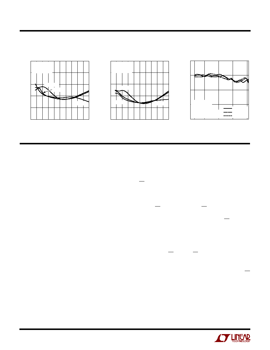
INL vs Output Rate
Resolution vs Output Rate
OUTPUT RATE (Hz)
0
TUE RESOLUTION (BITS)
16
18
20
40
24212 G28
14
12
10
10 20 30
50 60 70 80 90 100
V
CC
= 5V
V
REF
= 5V
F
O
= EXTERNAL
T
A
= ≠45
∞
C
T
A
= 25
∞
C
T
A
= 90
∞
C
OUTPUT RATE (Hz)
0
TUE RESOLUTION (BITS)
16
18
20
40
24212 G29
14
12
10
10 20 30
50 60 70 80 90 100
V
CC
= 3V
V
REF
= 2.5V
F
O
= EXTERNAL
T
A
= ≠45
∞
C
T
A
= 25
∞
C
T
A
= 90
∞
C
OUTPUT RATE (Hz)
0 7.5
EFFECTIVE RESOLUTION (BITS)
20
22
75
24212 G30
18
16
25
50
100
24
T
A
= 25
∞
C
T
A
= 90
∞
C
T
A
= ≠45
∞
C
V
CC
= 5V
V
REF
= 5V
f
O
= EXTERNAL
STANDARD DEVIATION
OF 100 SAMPLES
INL vs Output Rate
9
LTC2421/LTC2422
24212f
PI
N
FU
N
CTIO
N
S
U
U
U
SCK (Pin 9): Bidirectional Digital Clock Pin. In the Internal
Serial Clock Operation mode, SCK is used as digital output
for the internal serial interface clock during the data output
period. In the External Serial Clock Operation mode, SCK
is used as digital input for the external serial interface. An
internal pull-up current source is automatically activated
in Internal Serial Clock Operation mode. The Serial Clock
mode is determined by the level applied to SCK at power
up and the falling edge of CS.
F
O
(Pin 10): Frequency Control Pin. Digital input that
controls the ADC's notch frequencies and conversion
time. When the F
O
pin is connected to V
CC
(F
O
= V
CC
), the
converter uses its internal oscillator and the digital filter's
first null is located at 50Hz. When the F
O
pin is connected
to GND (F
O
= 0V), the converter uses its internal oscillator
and the digital filter's first null is located at 60Hz. When F
O
is driven by an external clock signal with a frequency f
EOSC
,
the converter uses this signal as its clock and the digital
filter first null is located at a frequency f
EOSC
/2560.
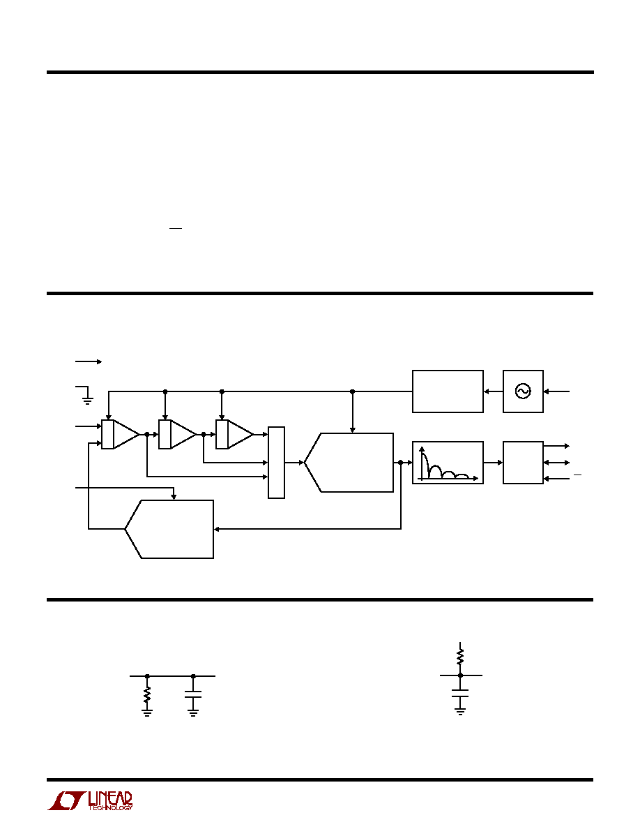
FU
N
CTIO
N
AL BLOCK DIAGRA
U
U
W
TEST CIRCUITS
3.4k
SDO
24212 TC01
Hi-Z TO V
OH
V
OL
TO V
OH
V
OH
TO Hi-Z
C
LOAD
= 20pF
3.4k
SDO
24212 TC02
Hi-Z TO V
OL
V
OH
TO V
OL
V
OL
TO Hi-Z
C
LOAD
= 20pF
V
CC
AUTOCALIBRATION
AND CONTROL
DAC
DECIMATING FIR
INTERNAL
OSCILLATOR
SERIAL
INTERFACE
ADC
GND
V
CC
V
IN
SDO
SCK
V
REF
CS
F
O
(INT/EXT)
24212 FD
10
LTC2421/LTC2422
24212f
APPLICATIO S I FOR ATIO
W
U
U
U
The LTC2421/LTC2422 are pin compatible with the
LTC2401/LTC2402. The devices are designed to allow the
user to incorporate either device in the same design with
no modifications. While the LTC2421/LTC2422 output word
length is 24 bits (as opposed to the 32-bit output of the
LTC2401/LTC2402), its output clock timing can be identi-
cal to the LTC2401/LTC2402. As shown in Figure 1, the
LTC2421/LTC2422 data output is concluded on the falling
edge of the 24th serial clock (SCK). In order to maintain
drop-in compatibility with the LTC2401/LTC2402, it is
possible to clock the LTC2421/LTC2422 with an additional
8 serial clock pulses. This results in 8 additional output bits
which are always logic HIGH.
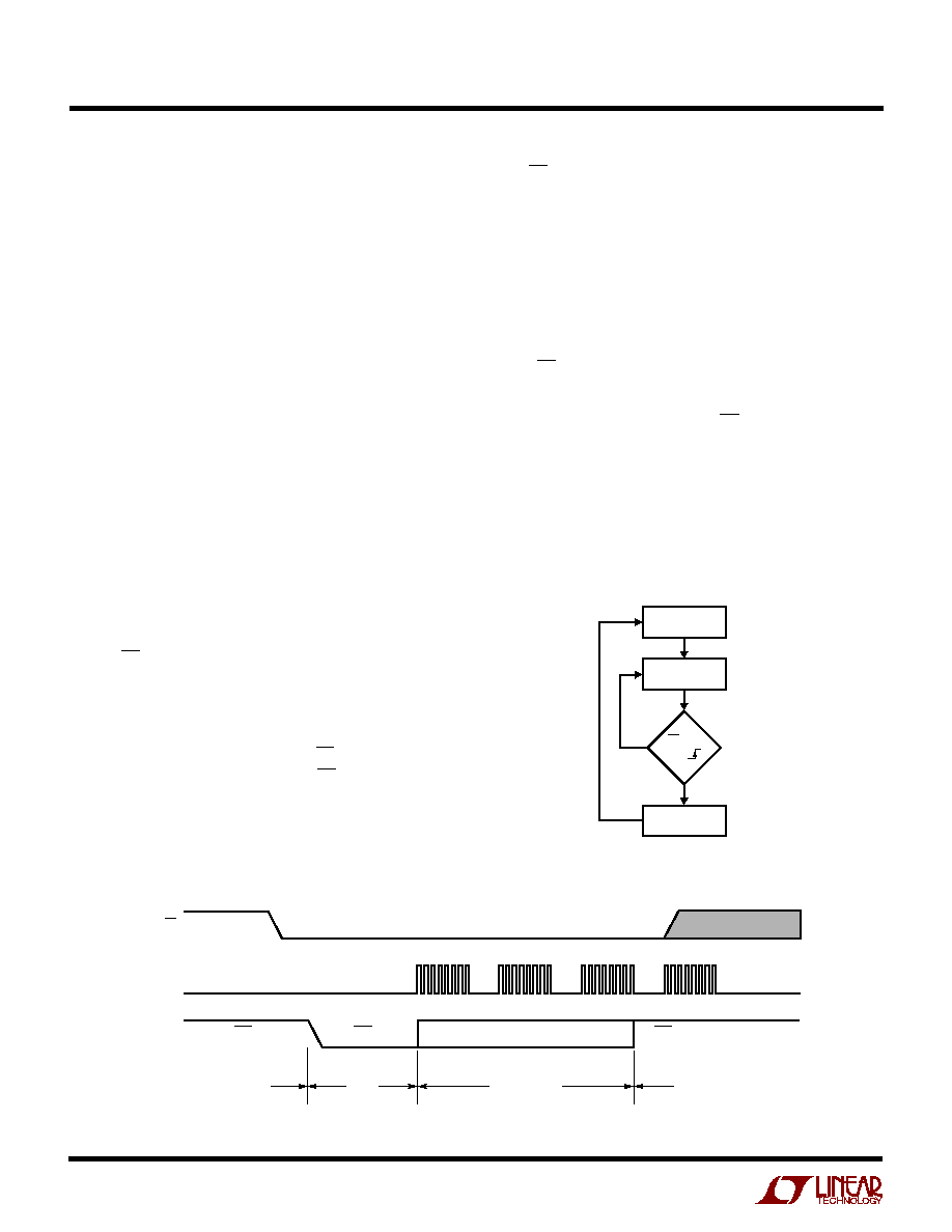
Converter Operation Cycle
The LTC2421/LTC2422 are low power, delta-sigma ana-
log-to-digital converters with an easy to use 3-wire serial
interface. Their operation is simple and made up of three
states. The converter operating cycle begins with the con-
version, followed by the sleep state and concluded with the
data output (see Figure 2). The 3-wire interface consists of
serial data output (SDO), a serial clock (SCK) and a chip
select (CS).
Initially, the LTC2421/LTC2422 perform a conversion. Once
the conversion is complete, the device enters the sleep
state. While in this sleep state, power consumption is re-
duced by an order of magnitude if CS is HIGH. The part
remains in the sleep state as long as CS is logic HIGH. The
conversion result is held indefinitely in a static shift regis-
ter while the converter is in the sleep state.
Figure 1. LTC2421/LTC2422 Compatible Timing with the LTC2401/LTC2402
CS
SCK
SDO
CONVERSION
SLEEP
8
8
8
8 (OPTIONAL)
EOC = 1
EOC = 1
LAST 8 BITS ALWAYS 1
EOC = 0
DATA OUT
4 STATUS BITS 20 DATA BITS
DATA OUTPUT
24212 F01
CONVERSION
CONVERT
SLEEP
DATA OUTPUT
24212 F02
0
1 CS AND
SCK
Figure 2. LTC2421/LTC2422 State Transition Diagram
Once CS is pulled LOW and SCK rising edge is applied, the
device begins outputting the conversion result. There is no
latency in the conversion result. The data output corre-
sponds to the conversion just performed. This result is
shifted out on the serial data out pin (SDO) under the
control of the serial clock (SCK). Data is updated on the
falling edge of SCK allowing the user to reliably latch data
on the rising edge of SCK, see Figure 4. The data output
state is concluded once 24 bits are read out of the ADC or
when CS is brought HIGH. The device automatically
initiates a new conversion and the cycle repeats.
Through timing control of the CS and SCK pins, the
LTC2421/LTC2422 offer several flexible modes of opera-
tion (internal or external SCK and free-running conver-
sion modes). These various modes do not require
programming configuration registers; moreover, they do
not disturb the cyclic operation described above. These
modes of operation are described in detail in the Serial
Interface Timing Modes section.
11
LTC2421/LTC2422
24212f
Conversion Clock
A major advantage delta-sigma converters offer over con-
ventional type converters is an on-chip digital filter (com-
monly known as Sinc or Comb filter). For high resolution,
low frequency applications, this filter is typically designed
to reject line frequencies of 50Hz or 60Hz plus their har-
monics. In order to reject these frequencies in excess of
110dB, a highly accurate conversion clock is required. The
LTC2421/LTC2422 incorporate an on-chip highly accu-
rate oscillator. This eliminates the need for external fre-
quency setting components such as crystals or oscilla-
tors. Clocked by the on-chip oscillator, the LTC2421/
LTC2422 reject line frequencies (50Hz or 60Hz
±
2%) a
minimum of 110dB.
Ease of Use
The LTC2421/LTC2422 data output has no latency, filter
settling or redundant data associated with the conver-
sion cycle. There is a one-to-one correspondence be-
tween the conversion and the output data. Therefore,
multiplexing an analog input voltage is easy.
The LTC2421/LTC2422 perform offset and full-scale cali-
brations every conversion cycle. This calibration is trans-
parent to the user and has no effect on the cyclic operation
described above. The advantage of continuous calibration
is extreme stability of offset and full-scale readings with
respect to time, supply voltage change and temperature
drift.
Power-Up Sequence
The LTC2421/LTC2422 automatically enter an internal reset
state when the power supply voltage V
CC
drops below
approximately 2.2V. This feature guarantees the integrity
of the conversion result and of the serial interface mode
selection which is performed at the initial power-up. (See
the 2-wire I/O sections in the Serial Interface Timing Modes
section.)
When the V
CC
voltage rises above this critical threshold,
the converter creates an internal power-on-reset (POR)
signal with duration of approximately 0.5ms. The POR
signal clears all internal registers. Following the POR sig-
nal, the LTC2421/LTC2422 start a normal conversion cycle
and follows the normal succession of states described
APPLICATIO S I FOR ATIO
W
U
U
U
above. The first conversion result following POR is accu-
rate within the specifications of the device.
Reference Voltage Range
The LTC2421/LTC2422 can accept a reference voltage (V
REF
= FS
SET
≠ ZS
SET
) from 0V to V
CC
. The converter output
noise is determined by the thermal noise of the front-end
circuits, and as such, its value in microvolts is nearly con-
stant with reference voltage. A decrease in reference volt-
age will not significantly improve the converter's effective
resolution. On the other hand, a reduced reference voltage
will improve the overall converter INL performance. The
recommended range for the LTC2421/LTC2422 voltage
reference is 100mV to V
CC
.
Input Voltage Range
The converter is able to accommodate system level offset
and gain errors as well as system level overrange situa-
tions due to its extended input range, see Figure 3. The
LTC2421/LTC2422 convert input signals within the ex-
tended input range of ≠ 0.125 ∑ V
REF
to 1.125 ∑ V
REF
(V
REF
= FS
SET
≠ ZS
SET
).
For large values of V
REF
(V
REF
= FS
SET
≠ ZS
SET
), this range
is limited by the absolute maximum voltage range of
≠ 0.3V to (V
CC
+ 0.3V). Beyond this range, the input ESD
protection devices begin to turn on and the errors due to
the input leakage current increase rapidly.
Input signals applied to V
IN
may extend below ground by
≠ 300mV and above V
CC
by 300mV. In order to limit any
Figure 3. LTC2421/LTC2422 Input Range
24212 F03
V
CC
+ 0.3V
FS
SET
+ 0.12V
REF
FS
SET
≠0.3V
(V
REF
= FS
SET
≠ ZS
SET
)
ZS
SET
≠ 0.12V
REF
ZS
SET
NORMAL
INPUT
RANGE
EXTENDED
INPUT
RANGE
ABSOLUTE
MAXIMUM
INPUT
RANGE
12
LTC2421/LTC2422
24212f
APPLICATIO S I FOR ATIO
W
U
U
U
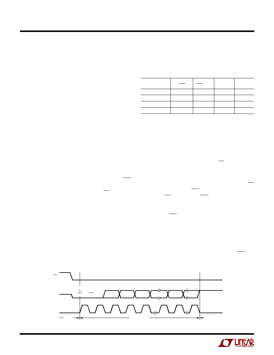
Figure 4. Output Data Timing
fault current, a resistor of up to 5k may be added in series
with the V
IN
pin without affecting the performance of the
device. In the physical layout, it is important to maintain
the parasitic capacitance of the connection between this
series resistance and the V
IN
pin as low as possible; there-
fore, the resistor should be located as close as practical to
the V
IN
pin. The effect of the series resistance on the con-
verter accuracy can be evaluated from the curves pre-
sented in the Analog Input/Reference Current section. In
addition, a series resistor will introduce a temperature de-
pendent offset error due to the input leakage current. A
1nA input leakage current will develop a 1ppm offset error
on a 5k resistor if V
REF
= 5V. This error has a very strong
temperature dependency.
Output Data Format
The LTC2421/LTC2422 serial output data stream is 24 bits
long. The first 4 bits represent status information indicat-
ing the sign, selected channel, input range and conversion
state. The next 20 bits are the conversion result, MSB first.
Bit 23 (first output bit) is the end of conversion (EOC)
indicator. This bit is available at the SDO pin during the
conversion and sleep states whenever the CS pin is LOW.
This bit is HIGH during the conversion and goes LOW
when the conversion is complete.
Bit 22 (second output bit) for the LTC2422, this bit is LOW
if the last conversion was performed on CH0 and HIGH for
CH1. This bit is always LOW for the LTC2421.
Bit 21 (third output bit) is the conversion result sign indi-
cator (SIG). If V
IN
is >0, this bit is HIGH. If V
IN
is <0, this
bit is LOW. The sign bit changes state during the zero code.
Bit 20 (fourth output bit) is the extended input range (EXR)
indicator. If the input is within the normal input range
0
V
IN
V
REF
, this bit is LOW. If the input is outside the
normal input range, V
IN
> V
REF
or V
IN
< 0, this bit is HIGH.
The function of these bits is summarized in Table 1.
Table 1. LTC2421/LTC2422 Status Bits
Bit 23
Bit 22
Bit 21
Bit 20
Input Range
EOC
CH0/CH1
SIG
EXR
V
IN
> V
REF
0
*0/1
1
1
0 < V
IN
V
REF
0
*0/1
1
0
V
IN
= 0
+
/0
≠
0
*0/1
1/0
0
V
IN
< 0
0
*0/1
0
1
*Bit 22 displays the channel number for the LTC2422. Bit 22 is always
0 for the LTC2421
Bit 19 (fifth output bit) is the most significant bit (MSB).
Bits 19-0 are the 20-bit conversion result MSB first.
Bit 0 is the least significant bit (LSB).
Data is shifted out of the SDO pin under control of the serial
clock (SCK), see Figure 4. Whenever CS is HIGH, SDO
remains high impedance and any SCK clock pulses are
ignored by the internal data out shift register.
In order to shift the conversion result out of the device, CS
must first be driven LOW. EOC is seen at the SDO pin of the
device once CS is pulled LOW. EOC changes real time from
HIGH to LOW at the completion of a conversion. This sig-
nal may be used as an interrupt for an external microcon-
troller. Bit 23 (EOC) can be captured on the first rising edge
of SCK. Bit 22 is shifted out of the device on the first falling
edge of SCK. The final data bit (Bit 0) is shifted out on the
falling edge of the 23rd SCK and may be latched on the
rising edge of the 24th SCK pulse. On the falling edge of the
24th SCK pulse, SDO goes HIGH indicating a new conver-
sion cycle has been initiated. This bit serves as EOC (Bit
23) for the next conversion cycle. Table 2 summarizes the
output data format.
MSB
EXT
SIG
CH0/CH1
1
2
3
4
5
19
20
24
BIT 0
BIT 19
BIT 4
LSB
20
BIT 20
BIT 21
BIT 22
SDO
SCK
CS
EOC
BIT 23
SLEEP
DATA OUTPUT
CONVERSION
24212 F04
Hi-Z
13
LTC2421/LTC2422
24212f
APPLICATIO S I FOR ATIO
W
U
U
U
As long as the voltage on the V
IN
pin is maintained within
the ≠ 0.3V to (V
CC
+ 0.3V) absolute maximum operating
range, a conversion result is generated for any input value
from ≠ 0.125 ∑ V
REF
to 1.125 ∑ V
REF
.
For input voltages
greater than 1.125 ∑ V
REF
, the conversion result is clamped
to the value corresponding to 1.125 ∑ V
REF
. For input volt-
ages below ≠ 0.125 ∑ V
REF
, the conversion result is clamped
to the value corresponding to ≠ 0.125 ∑ V
REF
.
Frequency Rejection Selection (F
O
Pin Connection)
The LTC2421/LTC2422 internal oscillator provides better
than 110dB normal mode rejection at the line frequency
and all its harmonics for 50Hz
±
2% or 60Hz
±
2%. For
60Hz rejection, F
O
(Pin 10) should be connected to GND
(Pin 6) while for 50Hz rejection the F
O
pin should be con-
nected to V
CC
(Pin 1).
The selection of 50Hz or 60Hz rejection can also be made
by driving F
O
to an appropriate logic level. A selection
change during the sleep or data output states will not
disturb the converter operation. If the selection is made
during the conversion state, the result of the conversion in
progress may be outside specifications but the following
conversions will not be affected.
When a fundamental rejection frequency different from
50Hz or 60Hz is required or when the converter must be
synchronized with an outside source, the LTC2421/
LTC2422 can operate with an external conversion clock.
The converter automatically detects the presence of an
external clock signal at the F
O
pin and turns off the internal
oscillator. The frequency f
EOSC
of the external signal must
be at least 2560Hz (1Hz notch frequency) to be detected.
The external clock signal duty cycle is not significant as
long as the minimum and maximum specifications for the
high and low periods t
HEO
and t
LEO
are observed.
While operating with an external conversion clock of a
frequency f
EOSC
, the LTC2421/LTC2422 provide better than
110dB normal mode rejection in a frequency range f
EOSC
/
2560
±
4% and its harmonics. The normal mode rejection
as a function of the input frequency deviation from f
EOSC
/
2560 is shown in Figure 5.
Whenever an external clock is not present at the F
O
pin, the
converter automatically activates its internal oscillator and
enters the Internal Conversion Clock mode. The LTC2421/
LTC2422 operation will not be disturbed if the change of
conversion clock source occurs during the sleep state or
during the data output state while the converter uses an
Table 2. LTC2421/LTC2422 Output Data Format
Bit 23
Bit 22*
Bit 21
Bit 20
Bit 19
Bit 18
Bit 17
Bit 16
Bit 15
...
Bit 0
Input Voltage
EOC
CH0/CH1
SIG
EXR
MSB
LSB
V
IN
> 9/8 ∑ V
REF
0
CH0/CH1
1
1
0
0
0
1
1
...
1
9/8 ∑ V
REF
0
CH0/CH1
1
1
0
0
0
1
1
...
1
V
REF
+ 1LSB
0
CH0/CH1
1
1
0
0
0
0
0
...
0
V
REF
0
CH0/CH1
1
0
1
1
1
1
1
...
1
3/4V
REF
+ 1LSB
0
CH0/CH1
1
0
1
1
0
0
0
...
0
3/4V
REF
0
CH0/CH1
1
0
1
0
1
1
1
...
1
1/2V
REF
+ 1LSB
0
CH0/CH1
1
0
1
0
0
0
0
...
0
1/2V
REF
0
CH0/CH1
1
0
0
1
1
1
1
...
1
1/4V
REF
+ 1LSB
0
CH0/CH1
1
0
0
1
0
0
0
...
0
1/4V
REF
0
CH0/CH1
1
0
0
0
1
1
1
...
1
0
+
/0
≠
0
CH0/CH1
1/0**
0
0
0
0
0
0
...
0
≠1LSB
0
CH0/CH1
0
1
1
1
1
1
1
...
1
≠1/8 ∑ V
REF
0
CH0/CH1
0
1
1
1
1
0
0
...
0
V
IN
< ≠1/8 ∑ V
REF
0
CH0/CH1
0
1
1
1
1
0
0
...
0
*Bit 22 is always 0 for the LTC2421 **The sign bit changes state during the 0 code.
14
LTC2421/LTC2422
24212f
external serial clock. If the change occurs during the con-
version state, the result of the conversion in progress may
be outside specifications but the following conversions
will not be affected. If the change occurs during the data
output state and the converter is in the Internal SCK mode,
the serial clock duty cycle may be affected but the serial
data stream will remain valid.
Table 3 summarizes the duration of each state as a func-
tion of F
O
.
SERIAL INTERFACE
The LTC2421/LTC2422 transmit the conversion results
and receives the start of conversion command through a
synchronous 3-wire interface. During the conversion and
sleep states, this interface can be used to assess the con-
verter status and during the data output state, it is used to
read the conversion result.
Serial Clock Input/Output (SCK)
The serial clock signal present on SCK (Pin 9) is used to
synchronize the data transfer. Each bit of data is shifted out
the SDO pin on the falling edge of the serial clock.
In the Internal SCK mode of operation, the SCK pin is an
output and the LTC2421/LTC2422 create their own serial
clock by dividing the internal conversion clock by 8. In the
External SCK mode of operation, the SCK pin is used as
input. The internal or external SCK mode is selected on
power-up and then reselected every time a HIGH-to-LOW
transition is detected at the CS pin. If SCK is HIGH or
floating at power-up or during this transition, the con-
verter enters the internal SCK mode. If SCK is LOW at
power-up or during this transition, the converter enters
the external SCK mode.
Serial Data Output (SDO)
The serial data output pin, SDO (Pin 8), drives the serial
data during the data output state. In addition, the SDO pin
is used as an end of conversion indicator during the con-
version and sleep states.
When CS (Pin 7) is HIGH, the SDO driver is switched to a
high impedance state. This allows sharing the serial
Table 3. LTC2421/LTC2422 State Duration
State
Operating Mode
Duration
CONVERT
Internal Oscillator
F
O
= LOW
133ms
(60Hz Rejection)
F
O
= HIGH
160ms
(50Hz Rejection)
External Oscillator
F
O
= External Oscillator
20510/f
EOSC
s
with Frequency f
EOSC
kHz
(f
EOSC
/2560 Rejection)
SLEEP
As Long As CS = HIGH Until CS = 0 and SCK
DATA OUTPUT
Internal Serial Clock
F
O
= LOW/HIGH
As Long As CS = LOW But Not Longer Than 1.28ms
(Internal Oscillator)
(24 SCK cycles)
F
O
= External Oscillator with
As Long As CS = LOW But Not Longer Than 192/f
EOSC
ms
Frequency f
EOSC
kHz
(24 SCK cycles)
External Serial Clock with
As Long As CS = LOW But Not Longer Than 24/f
SCK
ms
Frequency f
SCK
kHz
(24 SCK cycles)
APPLICATIO S I FOR ATIO
W
U
U
U
Figure 5. LTC2421/LTC2422 Normal Mode Rejection When
Using an External Oscillator of Frequency f
EOSC
INPUT FREQUENCY DEVIATION FROM NOTCH FREQUENCY (%)
≠12
≠8
≠4
0
4
8
12
REJECTION (dB)
24212 F05
≠60
≠70
≠80
≠90
≠100
≠110
≠120
≠130
≠140

15
LTC2421/LTC2422
24212f
interface with other devices. If CS is LOW during the con-
vert or sleep state, SDO will output EOC. If CS is LOW
during the conversion phase, the EOC bit appears HIGH on
the SDO pin. Once the conversion is complete, EOC goes
LOW. The device remains in the sleep state until the first
rising edge of SCK occurs while CS = 0. While in the sleep
state, the device is in a LOW power state if CS is HIGH.
Chip Select Input (CS)
The active LOW chip select, CS (Pin 7), is used to test the
conversion status and to enable the data output transfer as
described in the previous sections.
In addition, the CS signal can be used to trigger a new
conversion cycle before the entire serial data transfer has
been completed. The LTC2421/LTC2422 will abort any
serial data transfer in progress and start a new conversion
cycle anytime a LOW-to-HIGH transition is detected at the
CS pin after the converter has entered the data output state
(i.e., after the first rising edge of SCK occurs with CS = 0).
Finally, CS can be used to control the free-running modes
of operation, see Serial Interface Timing Modes section.
Grounding CS will force the ADC to continuously convert
at the maximum output rate selected by F
O
. Tying a ca-
pacitor to CS will reduce the output rate and power dissi-
pation by a factor proportional to the capacitor's value,
see Figures 13 to 15.
SERIAL INTERFACE TIMING MODES
The LTC2421/LTC2422's 3-wire interface is SPI and
MICROWIRE compatible. This interface offers several
flexible modes of operation. These include internal/exter-
nal serial clock, 2- or 3-wire I/O, single cycle conversion
and autostart. The following sections describe each of
these serial interface timing modes in detail. In all these
cases, the converter can use the internal oscillator (F
O
=
LOW or F
O
= HIGH) or an external oscillator connected to
the F
O
pin. Refer to Table 4 for a summary.
External Serial Clock, Single Cycle Operation
(SPI/MICROWIRE Compatible)
This timing mode uses an external serial clock to shift out
the conversion result and a CS signal to monitor and con-
trol the state of the conversion cycle, see Figure 6.
The serial clock mode is selected on the falling edge of CS.
To select the external serial clock mode, the serial clock pin
(SCK) must be LOW during each CS falling edge.
The serial data output pin (SDO) is Hi-Z as long as CS is
HIGH. At any time during the conversion cycle, CS may be
pulled LOW in order to monitor the state of the converter.
While CS is LOW, EOC is output to the SDO pin. EOC = 1
while a conversion is in progress and EOC = 0 if the device
is in the sleep state. Independent of CS, the device auto-
matically enters the sleep state once the conversion is
complete. While in the sleep state, power is reduced an
order of magnitude if CS is HIGH.
When the device is in the sleep state (EOC = 0), its
conversion result is held in an internal static shift register.
The device remains in the sleep state until the first rising
edge of SCK is seen while CS is LOW. Data is shifted out
the SDO pin on each falling edge of SCK. This enables
external circuitry to latch the output on the rising edge of
SCK. EOC can be latched on the first rising edge of SCK
and the last bit of the conversion result can be latched on
the 24th rising edge of SCK. On the 24th falling edge of
SCK, the device begins a new conversion. SDO goes HIGH
(EOC = 1) indicating a conversion is in progress.
Table 4. LTC2421/LTC2422 Interface Timing Modes
Conversion
Data
Connection
SCK
Cycle
Output
and
Configuration
Source
Control
Control
Waveforms
External SCK, Single Cycle Conversion
External
CS and SCK
CS and SCK
Figures 6, 7
External SCK, 2-Wire I/O
External
SCK
SCK
Figure 8
Internal SCK, Single Cycle Conversion
Internal
CS
CS
Figures 9, 10
Internal SCK, 2-Wire I/O, Continuous Conversion
Internal
Continuous
Internal
Figure 11
Internal SCK, Autostart Conversion
Internal
C
EXT
Internal
Figure 12
APPLICATIO S I FOR ATIO
W
U
U
U
16
LTC2421/LTC2422
24212f
APPLICATIO S I FOR ATIO
W
U
U
U
At the conclusion of the data cycle, CS may remain LOW
and EOC monitored as an end-of-conversion interrupt.
Alternatively, CS may be driven HIGH setting SDO to Hi-Z.
As described above, CS may be pulled LOW at any time in
order to monitor the conversion status.
Typically, CS remains LOW during the data output state.
However, the data output state may be aborted by pulling
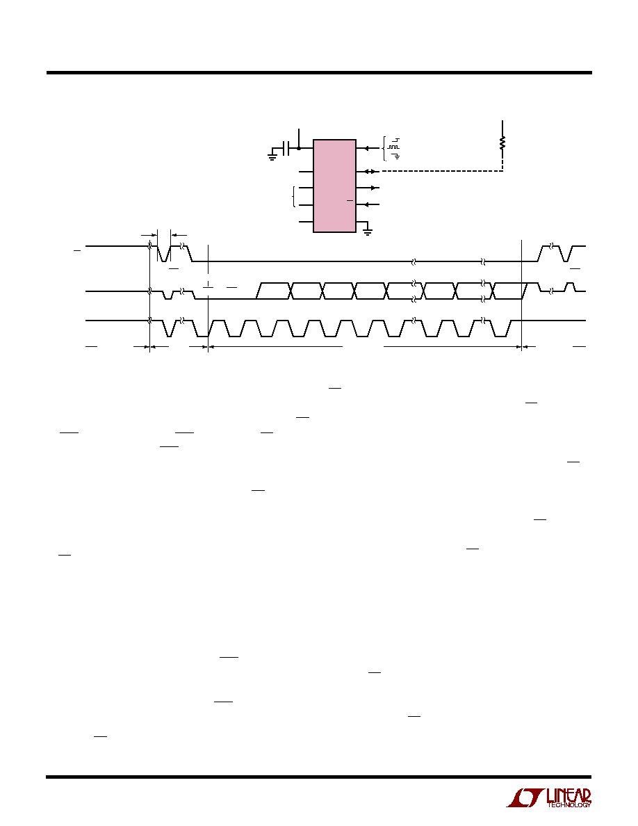
Figure 6. External Serial Clock, Single Cycle Operation
V
CC
F
O
FS
SET
ZS
SET
SCK
CH1
SDO
GND
CS
REFERENCE VOLTAGE
ZS
SET
+ 0.1V TO V
CC
0V TO FS
SET
≠ 100mV
CH0
= INTERNAL OSC/50Hz REJECTION
= EXTERNAL CLOCK SOURCE
= INTERNAL OSC/60Hz REJECTION
1
µ
F
1
10
9
8
7
6
2
3
4
5
2.7V TO 5.5V
LTC2422
V
CC
3-WIRE
SERIAL I/O
ANALOG INPUT RANGE
ZS
SET
≠ 0.12V
REF
TO
FS
SET
+ 0.12V
REF
(V
REF
= FS
SET
≠ ZS
SET
)
EOC
CH0/CH1
BIT 23
SDO
SCK
(EXTERNAL)
CS
TEST EOC
MSB
LSB
20
EXR
SIG
BIT 0
BIT 4
BIT 19
BIT 18
BIT 20
BIT 21
BIT 22
SLEEP
DATA OUTPUT
CONVERSION
24212 F06
CONVERSION
Hi-Z
Hi-Z
Hi-Z
TEST EOC
TEST EOC
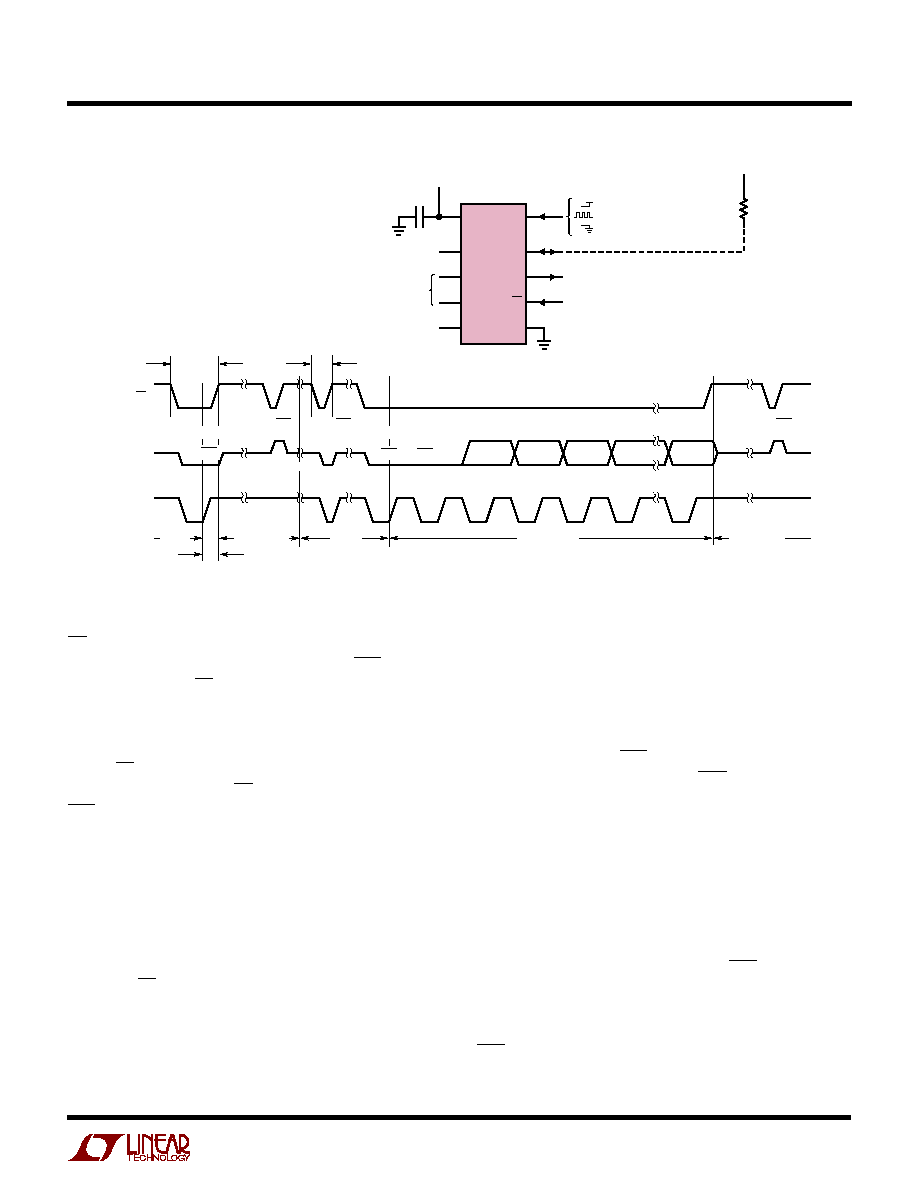
CS HIGH anytime between the first rising edge and the
24th falling edge of SCK, see Figure 7. On the rising edge
of CS, the device aborts the data output state and imme-
diately initiates a new conversion. This is useful for sys-
tems not requiring all 24 bits of output data, aborting an
invalid conversion cycle or synchronizing the start of a
conversion.
Figure 7. External Serial Clock, Reduced Data Output Length
V
CC
F
O
FS
SET
ZS
SET
SCK
CH1
SDO
GND
CS
REFERENCE VOLTAGE
ZS
SET
+ 0.1V TO V
CC
0V TO FS
SET
≠ 100mV
CH0
= INTERNAL OSC/50Hz REJECTION
= EXTERNAL CLOCK SOURCE
= INTERNAL OSC/60Hz REJECTION
1
µ
F
1
10
9
8
7
6
2
3
4
5
2.7V TO 5.5V
LTC2422
V
CC
3-WIRE
SERIAL I/O
ANALOG INPUT RANGE
ZS
SET
≠ 0.12V
REF
TO
FS
SET
+ 0.12V
REF
(V
REF
= FS
SET
≠ ZS
SET
)
SDO
SCK
(EXTERNAL)
CS
DATA OUTPUT
CONVERSION
SLEEP
SLEEP
TEST EOC
TEST EOC
DATA OUTPUT
Hi-Z
Hi-Z
Hi-Z
CONVERSION
24212 F07
MSB
EXR
SIG
BIT 8
BIT 19
BIT 9
BIT 20
BIT 21
BIT 22
EOC
CH0/CH1
BIT 23
BIT 0
EOC
Hi-Z
TEST EOC
17
LTC2421/LTC2422
24212f
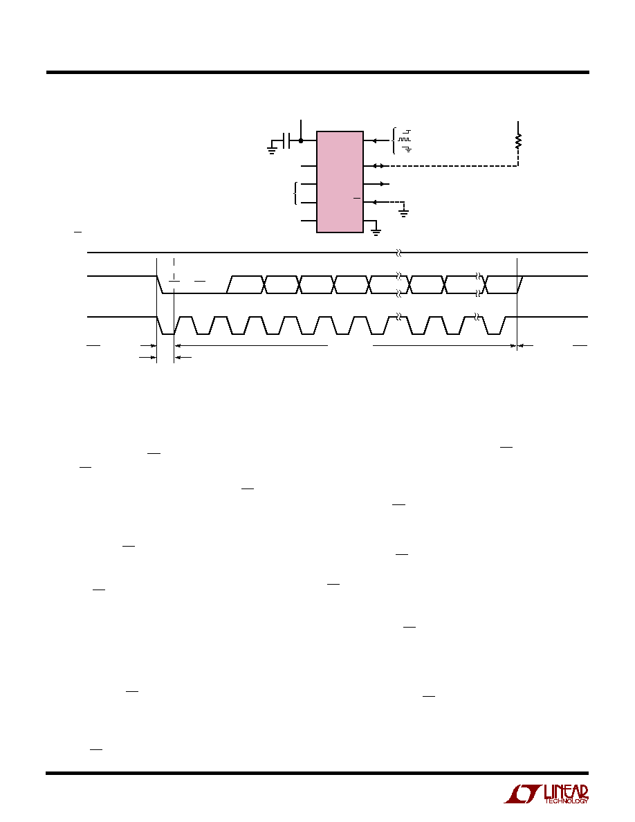
External Serial Clock, 2-Wire I/O
This timing mode utilizes a 2-wire serial I/O interface. The
conversion result is shifted out of the device by an exter-
nally generated serial clock (SCK) signal, see Figure 8. CS
may be permanently tied to ground (Pin 6), simplifying the
user interface or isolation barrier.
The external serial clock mode is selected at the end of the
power-on reset (POR) cycle. The POR cycle is concluded
approximately 0.5ms after V
CC
exceeds 2.2V. The level
applied to SCK at this time determines if SCK is internal or
external. SCK must be driven LOW prior to the end of POR
in order to enter the external serial clock timing mode.
Since CS is tied LOW, the end-of-conversion (EOC) can
be continuously monitored at the SDO pin during the
convert and sleep states. EOC may be used as an inter-
rupt to an external controller indicating the conversion
result is ready. EOC = 1 while the conversion is in progress
and EOC = 0 once the conversion enters the low power
sleep state. On the falling edge of EOC, the conversion
result is loaded into an internal static shift register. The
device remains in the sleep state until the first rising edge
of SCK. Data is shifted out the SDO pin on each falling
edge of SCK enabling external circuitry to latch data on
the rising edge of SCK. EOC can be latched on the first
rising edge of SCK. On the 24th falling edge of SCK, SDO
goes HIGH (EOC = 1) indicating a new conversion has
begun.
Internal Serial Clock, Single Cycle Operation
This timing mode uses an internal serial clock to shift out
the conversion result and a CS signal to monitor and con-
trol the state of the conversion cycle, see Figure 9.
In order to select the internal serial clock timing mode, the
serial clock pin (SCK) must be floating (Hi-Z) or pulled
HIGH prior to the falling edge of CS. The device will not
enter the internal serial clock mode if SCK is driven LOW
on the falling edge of CS. An internal weak pull-up resistor
is active on the SCK pin during the falling edge of CS;
therefore, the internal serial clock timing mode is auto-
matically selected if SCK is not externally driven.
The serial data output pin (SDO) is Hi-Z as long as CS is
HIGH. At any time during the conversion cycle, CS may be
pulled LOW in order to monitor the state of the converter.
Once CS is pulled LOW, SCK goes LOW and EOC is output
to the SDO pin. EOC = 1 while a conversion is in progress
and EOC = 0 if the device is in the sleep state.
When testing EOC, if the conversion is complete (EOC = 0),
the device will exit the sleep state and enter the data output
state if CS remains LOW. In order to prevent the device
from exiting the low power sleep state, CS must be pulled
APPLICATIO S I FOR ATIO
W
U
U
U
Figure 8. External Serial Clock, CS = 0 Operation
V
CC
F
O
FS
SET
ZS
SET
SCK
CH1
SDO
GND
CS
REFERENCE VOLTAGE
ZS
SET
+ 0.1V TO V
CC
0V TO FS
SET
≠ 100mV
CH0
= INTERNAL OSC/50Hz REJECTION
= EXTERNAL CLOCK SOURCE
= INTERNAL OSC/60Hz REJECTION
1
µ
F
1
10
9
2-WIRE SERIAL I/O
8
7
6
2
3
4
5
2.7V TO 5.5V
LTC2422
V
CC
ANALOG INPUT RANGE
ZS
SET
≠ 0.12V
REF
TO
FS
SET
+ 0.12V
REF
(V
REF
= FS
SET
≠ ZS
SET
)
EOC
CH0/CH1
BIT 23
SDO
SCK
(EXTERNAL)
CS
MSB
EXR
SIG
BIT 0
LSB
20
BIT 4
BIT 19
BIT 18
BIT 20
BIT 21
BIT 22
SLEEP
DATA OUTPUT
CONVERSION
24212 F08
CONVERSION
18
LTC2421/LTC2422
24212f
APPLICATIO S I FOR ATIO
W
U
U
U
HIGH before the first rising edge of SCK. In the internal
SCK timing mode, SCK goes HIGH and the device begins
outputting data at time t
EOCtest
after the falling edge of CS
(if EOC = 0) or t
EOCtest
after EOC goes LOW (if CS is LOW
during the falling edge of EOC). The value of t
EOCtest
is 23
µ
s
if the device is using its internal oscillator (F
0
= logic LOW
or HIGH). If F
O
is driven by an external oscillator of fre-
quency f
EOSC
, then t
EOCtest
is 3.6/f
EOSC
. If CS is pulled
HIGH before time t
EOCtest
, the device remains in the sleep
state. The conversion result is held in the internal static
shift register.
If CS remains LOW longer than t
EOCtest
, the first rising
edge of SCK will occur and the conversion result is serially
shifted out of the SDO pin. The data output cycle begins on
this first rising edge of SCK and concludes after the 24th
rising edge. Data is shifted out the SDO pin on each falling
edge of SCK. The internally generated serial clock is output
to the SCK pin. This signal may be used to shift the con-
version result into external circuitry. EOC can be latched
on the first rising edge of SCK and the last bit of the con-
version result on the 24th rising edge of SCK. After the
24th rising edge, SDO goes HIGH (EOC = 1), SCK stays
HIGH, and a new conversion starts.
Typically, CS remains LOW during the data output state.
However, the data output state may be aborted by pulling
CS HIGH anytime between the first and 24th rising edge of
SCK, see Figure 10. On the rising edge of CS, the device
aborts the data output state and immediately initiates a
new conversion. This is useful for systems not requiring
all 24 bits of output data, aborting an invalid conversion
cycle, or synchronizing the start of a conversion. If CS is
pulled HIGH while the converter is driving SCK LOW, the
internal pull-up is not available to restore SCK to a logic
HIGH state. This will cause the device to exit the internal
serial clock mode on the next falling edge of CS. This can
be avoided by adding an external 10k pull-up resistor to
the SCK pin or by never pulling CS HIGH when SCK is LOW.
Whenever SCK is LOW, the LTC2421/LTC2422's internal
pull-up at pin SCK is disabled. Normally, SCK is not exter-
nally driven if the device is in the internal SCK timing mode.
However, certain applications may require an external driver
on SCK. If this driver goes Hi-Z after outputting a LOW
signal, the LTC2421/LTC2422's internal pull-up remains
disabled. Hence, SCK remains LOW. On the next falling
edge of CS, the device is switched to the external SCK
timing mode. By adding an external 10k pull-up resistor to
SCK, this pin goes HIGH once the external driver goes
Hi-Z. On the next CS falling edge, the device will remain in
the internal SCK timing mode.
Figure 9. Internal Serial Clock, Single Cycle Operation
V
CC
10k
V
CC
F
O
FS
SET
ZS
SET
SCK
CH1
SDO
GND
CS
REFERENCE VOLTAGE
ZS
SET
+ 0.1V TO V
CC
0V TO FS
SET
≠ 100mV
CH0
= INTERNAL OSC/50Hz REJECTION
= EXTERNAL CLOCK SOURCE
= INTERNAL OSC/60Hz REJECTION
1
µ
F
1
10
9
8
7
6
2
3
4
5
2.7V TO 5.5V
LTC2422
V
CC
ANALOG INPUT RANGE
ZS
SET
≠ 0.12V
REF
TO
FS
SET
+ 0.12V
REF
(V
REF
= FS
SET
≠ ZS
SET
)
SDO
SCK
(INTERNAL)
CS
MSB
EXR
SIG
BIT 0
LSB
20
BIT 4
TEST EOC
BIT 19
BIT 18
BIT 20
BIT 21
BIT 22
EOC
CH0/CH1
BIT 23
SLEEP
DATA OUTPUT
CONVERSION
CONVERSION
24212 F09
<t
EOCtest
Hi-Z
Hi-Z
Hi-Z
Hi-Z
TEST EOC
19
LTC2421/LTC2422
24212f
A similar situation may occur during the sleep state when
CS is pulsed HIGH-LOW-HIGH in order to test the conver-
sion status. If the device is in the sleep state (EOC = 0), SCK
will go LOW. Once CS goes HIGH (within the time period
defined above as t
EOCtest
), the internal pull-up is activated.
For a heavy capacitive load on the SCK pin, the internal
pull-up may not be adequate to return SCK to a HIGH level
before CS goes low again. This is not a concern under
normal conditions where CS remains LOW after detecting
EOC = 0. This situation is easily overcome by adding an
external 10k pull-up resistor to the SCK pin.
Internal Serial Clock, 2-Wire I/O,
Continuous Conversion
This timing mode uses a 2-wire, all output (SCK and SDO)
interface. The conversion result is shifted out of the device
by an internally generated serial clock (SCK) signal, see
Figure 11. CS may be permanently tied to ground (Pin 6),
simplifying the user interface or isolation barrier.
The internal serial clock mode is selected at the end of the
power-on reset (POR) cycle. The POR cycle is concluded
approximately 0.5ms after V
CC
exceeds 2.2V. An internal
weak pull-up is active during the POR cycle; therefore, the
internal serial clock timing mode is automatically selected
if SCK is not externally driven LOW (if SCK is loaded such
that the internal pull-up cannot pull the pin HIGH, the ex-
ternal SCK mode will be selected).
During the conversion, the SCK and the serial data output
pin (SDO) are HIGH (EOC = 1). Once the conversion is
complete, SCK and SDO go LOW (EOC = 0) indicating the
conversion has finished and the device has entered the
sleep state. The part remains in the sleep state a minimum
amount of time (1/2 the internal SCK period) then imme-
diately begins outputting data. The data output cycle begins
on the first rising edge of SCK and ends after the 24th
rising edge. Data is shifted out the SDO pin on each falling
edge of SCK. The internally generated serial clock is out-
put to the SCK pin. This signal may be used to shift the
conversion result into external circuitry. EOC can be latched
on the first rising edge of SCK and the last bit of the
conversion result can be latched on the 24th rising edge
of SCK. After the 24th rising edge, SDO goes HIGH
(EOC = 1) indicating a new conversion is in progress. SCK
remains HIGH during the conversion.
Figure 10. Internal Serial Clock, Reduced Data Output Length
APPLICATIO S I FOR ATIO
W
U
U
U
V
CC
10k
V
CC
F
O
FS
SET
ZS
SET
SCK
CH1
SDO
GND
CS
REFERENCE VOLTAGE
ZS
SET
+ 0.1V TO V
CC
0V TO FS
SET
≠ 100mV
CH0
= INTERNAL OSC/50Hz REJECTION
= EXTERNAL CLOCK SOURCE
= INTERNAL OSC/60Hz REJECTION
1
µ
F
1
10
9
8
7
6
2
3
4
5
2.7V TO 5.5V
LTC2422
V
CC
ANALOG INPUT RANGE
ZS
SET
≠ 0.12V
REF
TO
FS
SET
+ 0.12V
REF
(V
REF
= FS
SET
≠ ZS
SET
)
SDO
SCK
(INTERNAL)
CS
> t
EOCtest
MSB
EXR
SIG
BIT 8
TEST EOC
TEST EOC
BIT 19
BIT 18
BIT 20
BIT 21
BIT 22
EOC
CH0/CH1
BIT 23
EOC
BIT 0
SLEEP
DATA OUTPUT
Hi-Z
Hi-Z
Hi-Z
Hi-Z
Hi-Z
DATA OUTPUT
CONVERSION
CONVERSION
SLEEP
24212 F10
<t
EOCtest
TEST EOC
20
LTC2421/LTC2422
24212f
Internal Serial Clock, Autostart Conversion
This timing mode is identical to the internal serial clock,
2-wire I/O described above with one additional feature.
Instead of grounding CS, an external timing capacitor is
tied to CS.
While the conversion is in progress, the CS pin is held
HIGH by an internal weak pull-up. Once the conversion is
complete, the device enters the low power sleep state and
an internal 25nA current source begins discharging the
capacitor tied to CS, see Figure 12. The time the converter
spends in the sleep state is determined by the value of the
external timing capacitor, see Figures 13 and 14. Once the
voltage at CS falls below an internal threshold (
1.4V), the
device automatically begins outputting data. The data out-
put cycle begins on the first rising edge of SCK and ends
on the 24th rising edge. Data is shifted out the SDO pin on
each falling edge of SCK. The internally generated serial
clock is output to the SCK pin. This signal may be used to
shift the conversion result into external circuitry. After the
24th rising edge, CS is pulled HIGH and a new conversion
is immediately started. This is useful in applications re-
quiring periodic monitoring and ultralow power. Figure 15
shows the average supply current as a function of capaci-
tance on CS.
It should be noticed that the external capacitor discharge
current is kept very small in order to decrease the con-
verter power dissipation in the sleep state. In the autostart
mode, the analog voltage on the CS pin cannot be
observed without disturbing the converter operation
using a regular oscilloscope probe. When using this con-
figuration, it is important to minimize the external leakage
current at the CS pin by using a low leakage external ca-
pacitor and properly cleaning the PCB surface.
The internal serial clock mode is selected every time the
voltage on the CS pin crosses an internal threshold volt-
age. An internal weak pull-up at the SCK pin is active while
CS is discharging; therefore, the internal serial clock tim-
ing mode is automatically selected if SCK is floating. It is
important to ensure there are no external drivers pulling
SCK LOW while CS is discharging.
DIGITAL SIGNAL LEVELS
The LTC2421/LTC2422's digital interface is easy to use.
Its digital inputs (F
O
, CS and SCK in External SCK mode of
operation) accept standard TTL/CMOS logic levels and the
internal hysteresis receivers can tolerate edge rates as
slow as 100
µ
s. However, some considerations are required
Figure 11. Internal Serial Clock, Continuous Operation
APPLICATIO S I FOR ATIO
W
U
U
U
V
CC
F
O
FS
SET
ZS
SET
SCK
CH1
SDO
GND
CS
REFERENCE VOLTAGE
ZS
SET
+ 0.1V TO V
CC
0V TO FS
SET
≠ 100mV
CH0
= INTERNAL OSC/50Hz REJECTION
= EXTERNAL CLOCK SOURCE
= INTERNAL OSC/60Hz REJECTION
1
µ
F
1
10
9
8
7
6
2
3
4
5
2.7V TO 5.5V
LTC2422
V
CC
V
CC
10k
ANALOG INPUT RANGE
ZS
SET
≠ 0.12V
REF
TO
FS
SET
+ 0.12V
REF
(V
REF
= FS
SET
≠ ZS
SET
)
SDO
SCK
(INTERNAL)
CS
LSB
20
MSB
EXR
SIG
BIT 4
BIT 0
BIT 19
BIT 18
BIT 20
BIT 21
BIT 22
EOC
CH0/CH1
BIT 23
SLEEP
DATA OUTPUT
CONVERSION
CONVERSION
24212 F11
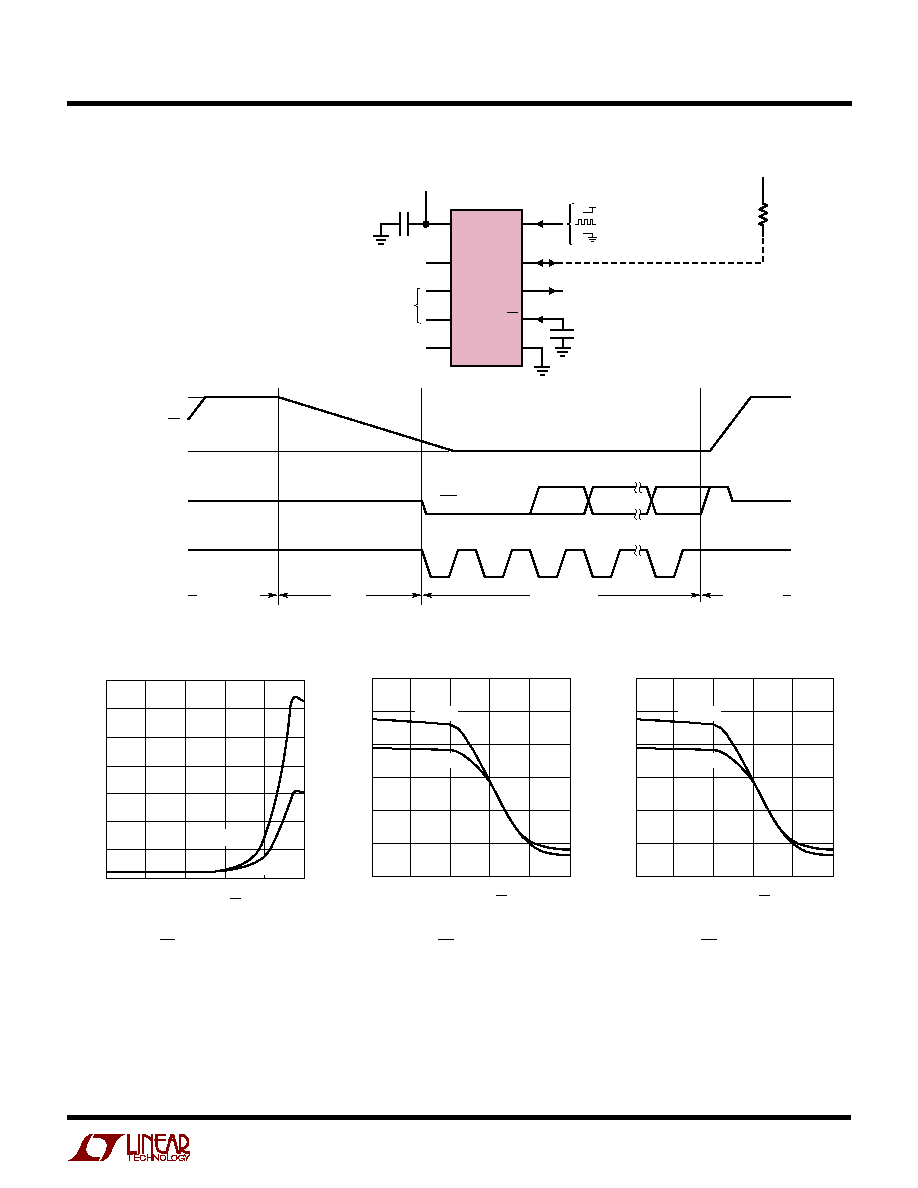
21
LTC2421/LTC2422
24212f
APPLICATIO S I FOR ATIO
W
U
U
U
Figure 12. Internal Serial Clock, Autostart Operation
V
CC
F
O
FS
SET
ZS
SET
SCK
CH1
SDO
GND
CS
REFERENCE VOLTAGE
ZS
SET
+ 0.1V TO V
CC
0V TO FS
SET
≠ 100mV
CH0
= INTERNAL OSC/50Hz REJECTION
= EXTERNAL CLOCK SOURCE
= INTERNAL OSC/60Hz REJECTION
1
µ
F
1
10
9
8
7
6
C
EXT
2
3
4
5
2.7V TO 5.5V
LTC2422
V
CC
V
CC
10k
ANALOG INPUT RANGE
ZS
SET
≠ 0.12V
REF
TO
FS
SET
+ 0.12V
REF
(V
REF
= FS
SET
≠ ZS
SET
)
SDO
Hi-Z
Hi-Z
SCK
(INTERNAL)
CS
V
CC
GND
2420 F12
BIT 0
SIG
BIT 21
BIT 22
SLEEP
DATA OUTPUT
CONVERSION
CONVERSION
EOC
BIT 23
Figure 13. CS Capacitance vs t
SAMPLE
Figure 14. CS Capacitance
vs Output Rate
CAPACITANCE ON CS (pF)
1
5
6
7
1000
10000
24212 F13
4
3
10
100
100000
2
1
0
t
SAMPLE
(SEC)
V
CC
= 5V
V
CC
= 3V
CAPACITANCE ON CS (pF)
1
0
SUPPLY CURRENT (
µ
A
RMS
)
50
100
150
200
250
300
10
100
1000
10000
24212 F15
100000
V
CC
= 5V
V
CC
= 3V
to take advantage of exceptional accuracy and low supply
current.
The digital output signals (SDO and SCK in Internal SCK
mode of operation) are less of a concern because they are
not generally active during the conversion state.
In order to preserve the LTC2421/LTC2422's accuracy, it
is very important to minimize the ground path impedance
which may appear in series with the input and/or reference
signal and to reduce the current which may flow through
this path. The GND pin should be connected to a low
CAPACITANCE ON CS (pF)
1
0
SUPPLY CURRENT (
µ
A
RMS
)
50
100
150
200
250
300
10
100
1000
10000
24212 F15
100000
V
CC
= 5V
V
CC
= 3V
Figure 15. CS Capacitance
vs Supply Current
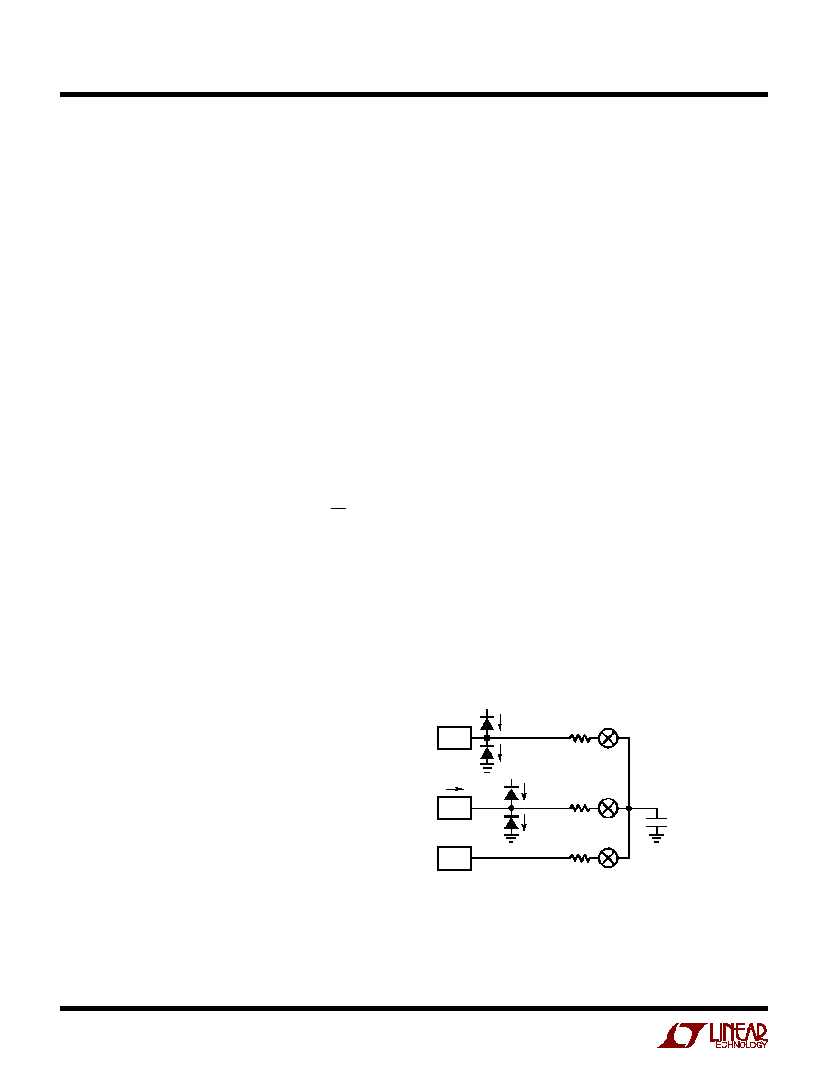
22
LTC2421/LTC2422
24212f
resistance ground plane through a minimum length trace.
The use of multiple via holes is recommended to further
reduce the connection resistance.
In an alternative configuration, the GND pin of the con-
verter can be the single-point-ground in a single point
grounding system. The input signal ground, the reference
signal ground, the digital drivers ground (usually the digi-
tal ground) and the power supply ground (the analog
ground) should be connected in a star configuration with
the common point located as close to the GND pin as
possible.
The power supply current during the conversion state
should be kept to a minimum. This is achieved by restrict-
ing the number of digital signal transitions occurring dur-
ing this period.
While a digital input signal is in the range 0.5V to
(V
CC
≠ 0.5V), the CMOS input receiver draws additional
current from the power supply. It should be noted that,
when any one of the digital input signals (F
O
, CS and SCK
in External SCK mode of operation) is within this range, the
LTC2421/LTC2422 power supply current may increase
even if the signal in question is at a valid logic level. For
micropower operation and in order to minimize the poten-
tial errors due to additional ground pin current, it is recom-
mended to drive all digital input signals to full CMOS levels
[V
IL
< 0.4V and V
OH
> (V
CC
≠ 0.4V)].
Severe ground pin current disturbances can also occur
due to the undershoot of fast digital input signals. Under-
shoot and overshoot can occur because of the imped-
ance mismatch at the converter pin when the transition
time of an external control signal is less than twice the
propagation delay from the driver to LTC2421/LTC2422.
For reference, on a regular FR-4 board, signal propaga-
tion velocity is approximately 183ps/inch for internal
traces and 170ps/inch for surface traces. Thus, a driver
generating a control signal with a minimum transition
time of 1ns must be connected to the converter pin through
a trace shorter than 2.5 inches. This problem becomes
particularly difficult when shared control lines are used
and multiple reflections may occur. The solution is to
carefully terminate all transmission lines close to their
characteristic impedance.
APPLICATIO S I FOR ATIO
W
U
U
U
Parallel termination near the LTC2421/LTC2422 pin will
eliminate this problem but will increase the driver power
dissipation. A series resistor between 27
and 56
placed
near the driver or near the LTC2421/LTC2422 pin will also
eliminate this problem without additional power dissipa-
tion. The actual resistor value depends upon the trace
impedance and connection topology.
Driving the Input and Reference
The analog input and reference of the typical delta-sigma
analog-to-digital converter are applied to a switched ca-
pacitor network. This network consists of capacitors switch-
ing between the analog input (V
IN
), ZS
SET
(Pin 5) and FS
SET
(Pin 2). The result is small current spikes seen at both V
IN
and V
REF
. A simplified input equivalent circuit is shown in
Figure 16.
The key to understanding the effects of this dynamic input
current is based on a simple first order RC time constant
model. Using the internal oscillator, the LTC2421/
LTC2422's internal switched capacitor network is clocked
at 153,600Hz corresponding to a 6.5
µ
s sampling period.
Fourteen time constants are required each time a capacitor
is switched in order to achieve 1ppm settling accuracy.
Therefore, the equivalent time constant at V
IN
and V
REF
should be less than 6.5
µ
s/14 = 460ns in order to achieve
1ppm accuracy.
Figure 16. LTC2421/LTC2422 Equivalent Analog Input Circuit
V
REF
V
IN
V
CC
R
SW
5k
AVERAGE INPUT CURRENT:
I
IN
= 0.25(V
IN
≠ 0.5 ∑ V
REF
)fC
EQ
I
REF(LEAK)
I
REF(LEAK)
V
CC
R
SW
5k
C
EQ
1pF (TYP)
R
SW
5k
I
IN(LEAK)
I
IN
24212 F16
I
IN(LEAK)
SWITCHING FREQUENCY
f = 153.6kHz FOR INTERNAL OSCILLATOR (f
O
= LOGIC LOW OR HIGH)
f = f
EOSC
FOR EXTERNAL OSCILLATORS
GND
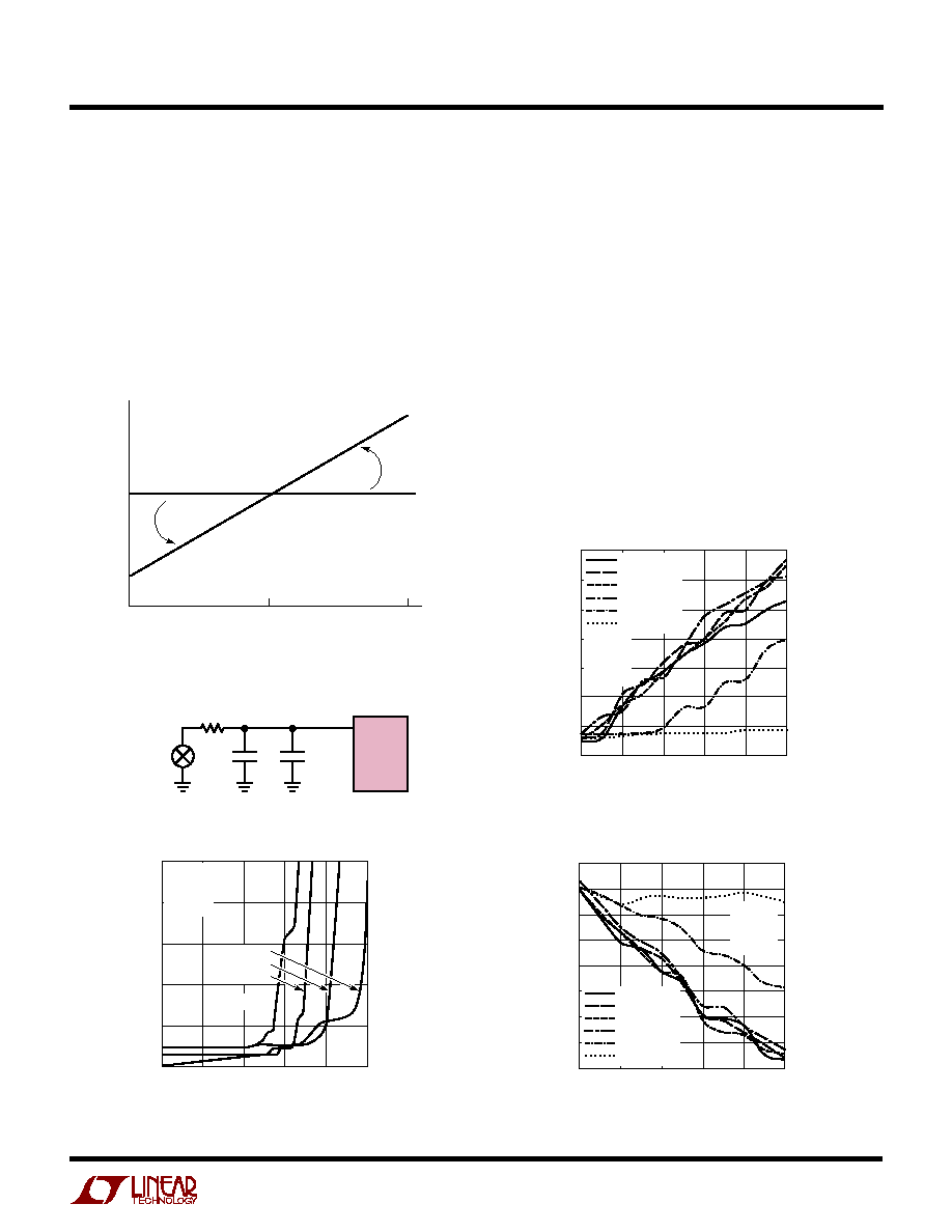
23
LTC2421/LTC2422
24212f
Input Current (V
IN
)
If complete settling occurs on the input, conversion re-
sults will be uneffected by the dynamic input current. If the
settling is incomplete, it does not degrade the linearity
performance of the device. It simply results in an offset/
full-scale shift, see Figure 17. To simplify the analysis of
input dynamic current, two separate cases are assumed:
large capacitance at V
IN
(C
IN
> 0.01
µ
F) and small capaci-
tance at V
IN
(C
IN
< 0.01
µ
F).
If the total capacitance at V
IN
(see Figure 18) is small
(< 0.01
µ
F), relatively large external source resistances (up
to 80k for 20pF parasitic capacitance) can be tolerated
without any offset/full-scale error. Figures 19 and 20 show
a family of offset and full-scale error curves for various
small valued input capacitors (C
IN
< 0.01
µ
F) as a function
of input source resistance.
For large input capacitor values (C
IN
> 0.01
µ
F), the input
spikes are averaged by the capacitor into a DC current. The
gain shift becomes a linear function of input source resis-
tance independent of input capacitance, see Figures 21
and 22. The equivalent input impedance is 16.6M
. This
results in
±
150nA of input dynamic current at the extreme
values of V
IN
(V
IN
= 0V and V
IN
= V
REF
, when V
REF
= 5V).
This corresponds to a 0.3ppm shift in offset and full-scale
readings for every 10
of input source resistance.
APPLICATIO S I FOR ATIO
W
U
U
U
Figure 18. An RC Network at V
IN
Figure 19. Offset vs R
SOURCE
(Small C)
Figure 17. Offset/Full-Scale Shift
ZS
SET
TUE
V
IN
24212 F17
FS
SET
C
IN
24212 F17
INTPUT
SIGNAL
SOURCE
R
SOURCE
V
IN
LTC2421/
LTC2422
C
PAR
20pF
R
SOURCE
(
)
1
OFFSET ERROR (ppm)
30
40
50
10k
24212 F19
20
10
0
10
100
1k
100k
V
CC
= 5V
V
REF
= 5V
V
IN
= 0V
T
A
= 25
∞
C
C
IN
= 100pF
C
IN
= 1000pF
C
IN
= 0pF
C
IN
= 0.01
µ
F
Figure 20. Offset vs R
SOURCE
(Large C)
Figure 21. Full-Scale Error vs R
SOURCE
(Large C)
R
SOURCE
(
)
0
25
30
35
600
800
24212 F20
20
15
200
400
1000
10
5
0
OFFSET ERROR (ppm)
C
IN
= 22
µ
F
C
IN
= 10
µ
F
C
IN
= 1
µ
F
C
IN
= 0.1
µ
F
C
IN
= 0.01
µ
F
C
IN
= 0.001
µ
F
V
CC
= 5V
V
REF
= 5V
V
IN
= 0V
T
A
= 25
∞
C
R
SOURCE
(
)
0
FULL-SCALE ERROR (ppm)
≠20
≠15
≠10
600
1000
24212 F21
≠25
≠30
≠35
200
400
800
≠5
0
5
C
IN
= 22
µ
F
C
IN
= 10
µ
F
C
IN
= 1
µ
F
C
IN
= 0.1
µ
F
C
IN
= 0.01
µ
F
C
IN
= 0.001
µ
F
V
CC
= 5V
V
REF
= 5V
V
IN
= 0V
T
A
= 25
∞
C
24
LTC2421/LTC2422
24212f
In addition to the input current spikes, the input ESD pro-
tection diodes have a temperature dependent leakage cur-
rent. This leakage current, nominally 1nA (
±
100nA max),
results in a fixed offset shift of 10
µ
V for a 10k source
resistance.
The effect of input leakage current is evident for C
IN
= 0 in
Figures 19 and 22. A leakage current of 3nA results in a
150
µ
V (30ppm) error for a 50k source resistance. As
R
SOURCE
gets larger, the switched capacitor input current
begins to dominate.
Reference Current (V
REF
)
Similar to the analog input, the reference input has a dy-
namic input current. This current has negligible effect on
the offset. However, the reference current at V
IN
= V
REF
is
similar to the input current at full-scale. For large values of
reference capacitance (C
VREF
> 0.01
µ
F), the full-scale er-
ror shift is 0.03ppm/
of external reference resistance
independent of the capacitance at V
REF
, see Figure 23. If
the capacitance tied to V
REF
is small (C
VREF
< 0.01
µ
F), an
input resistance of up to 80k (20pF parasitic capacitance
at V
REF
) may be tolerated, see Figure 24.
Unlike the analog input, the integral nonlinearity of the
device can be degraded with excessive external RC time
constants tied to the reference input. If the capacitance at
node V
REF
is small (C
VREF
< 0.01
µ
F), the reference input
can tolerate large external resistances without reduction
in INL, see Figure 25. If the external capacitance is large
(C
VREF
> 0.01
µ
F), the linearity will be degraded by
APPLICATIO S I FOR ATIO
W
U
U
U
R
SOURCE
(
)
1
≠50
FULL-SCALE ERROR (ppm)
≠40
≠30
≠20
≠10
0
10
10
100
1k
10k
24212 F22
100k
V
CC
= 5V
V
REF
= 5V
V
IN
= 5V
T
A
= 25
∞
C
C
IN
= 0.01
µ
F
C
IN
= 100pF
C
IN
= 1000pF
C
IN
= 0pF
Figure 22. Full-Scale Error vs R
SOURCE
(Small C)
Figure 23. Full-Scale Error vs R
VREF
(Large C)
Figure 24. Full-Scale Error vs R
VREF
(Small C)
RESISTANCE AT V
REF
(
)
0
40
50
60
600
800
24212 F23
30
20
200
400
1000
10
0
≠10
FULL-SCALE ERROR (ppm)
C
VREF
= 22
µ
F
C
VREF
= 10
µ
F
C
VREF
= 1
µ
F
C
VREF
= 0.1
µ
F
C
VREF
= 0.01
µ
F
C
VREF
= 0.001
µ
F
V
CC
= 5V
V
REF
= 5V
V
IN
= 5V
T
A
= 25
∞
C
RESISTANCE AT V
REF
(
)
1
300
400
500
1k
10k
24212 F24
200
100
10
100
100k
0
≠100
≠200
FULL-SCALE ERROR (ppm)
V
CC
= 5V
V
REF
= 5V
V
IN
= 5V
T
A
= 25
∞
C
C
VREF
= 0.01
µ
F
C
VREF
= 100pF
C
VREF
= 1000pF
C
VREF
= 0pF
Figure 25. INL Error vs R
VREF
(Small C)
RESISTANCE AT V
REF
(
)
1
30
40
50
1k
10k
24212 F25
20
10
10
100
100k
0
≠10
≠20
INL ERROR (ppm)
V
CC
= 5V
V
REF
= 5V
T
A
= 25
∞
C
C
VREF
= 0.01
µ
F
C
VREF
= 1000pF
C
VREF
= 0pF
C
VREF
= 100pF
25
LTC2421/LTC2422
24212f
0.015ppm/
independent of capacitance at V
REF
, see
Figure 26.
In addition to the dynamic reference current, the V
REF
ESD
protection diodes have a temperature dependent leakage
current. This leakage current, nominally 1nA (
±
10nA max),
results in a fixed full-scale shift of 10
µ
V for a 10k source
resistance.
APPLICATIO S I FOR ATIO
W
U
U
U
The modulator contained within the LTC2421/LTC2422
can handle large-signal level perturbations without satu-
rating. Signal levels up to 40% of V
REF
do not saturate the
analog modulator. These signals are limited by the input
ESD protection to 300mV below ground and 300mV above
V
CC
.
Simple Basic Program for Interfacing to the
LTC2421/LTC2422
Figure 26. INL Error vs R
VREF
(Large C)
RESISTANCE AT V
REF
(
)
0
6
8
10
600
800
24212 F26
4
2
≠2
≠4
≠6
≠8
≠10
200
400
1000
0
INL ERROR (ppm)
C
VREF
= 22
µ
F
C
VREF
= 10
µ
F
C
VREF
= 1
µ
F
C
VREF
= 0.1
µ
F
C
VREF
= 0.01
µ
F
C
VREF
= 0.001
µ
F
V
CC
= 5V
V
REF
= 5V
T
A
= 25
∞
C
ANTIALIASING
One of the advantages delta-sigma ADCs offer over con-
ventional ADCs is on-chip digital filtering. Combined with
a large oversampling ratio, the LTC2421/LTC2422 signifi-
cantly simplify antialiasing filter requirements.
The digital filter provides very high rejection except at
integer multiples of the modulator sampling frequency
(f
S
), see Figure 27. The modulator sampling frequency is
256 ∑ F
O
, where F
O
is the notch frequency (typically 50Hz
or 60Hz). The bandwidth of signals not rejected by the
digital filter is narrow (
0.2%) compared to the band-
width of the frequencies rejected.
As a result of the oversampling ratio (256) and the digital
filter, minimal (if any) antialias filtering is required in front
of the LTC2421/LTC2422. If passive RC components are
placed in front of the LTC2421/LTC2422, the input dy-
namic current should be considered (see Input Current
section). In cases where large effective RC time constants
are used, an external buffer amplifier may be required to
minimize the effects of input dynamic current.
Figure 27. Sinc
4
Filter Rejection
INPUT FREQUENCY
0
≠60
≠40
0
24212 F27
≠80
≠100
f
S
/2
f
S
≠120
≠140
≠20
REJECTION (dB)
SCK
DTR
PC
SERIAL
PORT
CTS
RTS
SDO
LTC2421
LTC2422
CS
24212 F28
V
REF
V
IN
GND
Figure 28
"TINY.BAS V1.0 Copyright (C) 2000 by J. A. Dutra and LTC, All rights reseved'
NOTE this program generates 32 SCK's for compatibility to 24-bit parts
'For use with most LTC24xy demo boards
designed for the PC Com Port, QBASIC
'Outputs are chan%,signneg%,d2400 (magnitude), PPM, and v (volts)
CLS : ON ERROR GOTO 4970
cport = 1: REM INPUT "com port number "; cport
GOSUB 1900: timestart$ = TIME$
mcr% = port + 4: msr% = port + 6
COLOR 15: LOCATE 3, 1: PRINT "Hit any key to stop... ";
FOR np = 1 TO 2000: OUT port, c0%: NEXT np: 'Power Via TxD
DO: '-------------------------START LOOP here--------

26
LTC2421/LTC2422
24212f
APPLICATIO S I FOR ATIO
W
U
U
U
nummeas = nummeas + c1%
LOCATE 2, 2: PRINT "Scan#="; nummeas; " "; DATE$; " "; TIME$;
OUT mcr%, c0%: 'Initialize SCLK=0
k1 = km: d2400 = 0: chan% = c0%: signneg% = c0%
FOR bita% = 31 TO 0 STEP -1: v31 = 1
148 GOSUB 2200: v31 = v31 + 1
150 IF bita% = 31 THEN GOTO 152 ELSE 156
152 IF dfrm% = c0% THEN GOTO 156
155 IF v31 > 2 THEN LOCATE 16, 16: OUT port, c0%: PRINT "waiting for eoc":
IF v31 < 20000 THEN IF dfrm% = c1% THEN GOTO 148
IF dfrm% = 1 THEN LOCATE 17, 16: PRINT "Timed out on EOC,not fatal"
FOR bs = 1 TO 32: ' never got an eoc => clock it 32 times
GOSUB 2000: NEXT bs: GOTO 1800
156 LOCATE 16, 16: PRINT"
": GOSUB 2000
IF bita% = 30 THEN 161 ELSE 171 ' CHANNEL BIT !!!!!!!!!!!!!!!
161 IF dfrm% = c1% THEN chan% = c1%: ch1% = c0%
IF dfrm% = c0% THEN chan% = c0%: ch1% = ch1% + c1%
IF ch1% > c4% THEN GOSUB 3700: ch1% = c1%
171 IF bita% = 29 THEN IF dfrm% = c0% THEN signneg% = c1%: ' NEG
IF bita% <= 28 THEN d2400 = d2400 + (dfrm% * k1): k1 = k1 / c2%
NEXT bita%: k1 = 1: digin% = c0%: 'MATH BELOW
1600 PPM = (d2400 / km) * kn: rw% = 6: hz% = (chan% * 20) + 1
IF signneg% = c1% THEN 1700 ELSE 1705
1700 IF d2400 <> c0% THEN PPM = (PPM - 2000000)
1705 LOCATE rw%, hz%: PRINT PPM; " "; : LOCATE rw%, hz% + 11:
PRINT "PPM";
LOCATE rw% + 1, (chan% * 20) + 1: GOSUB 3800: 'THIS WORKS!
1800 LOOP WHILE INKEY$ = "": REM Works with "DO"
GOTO 5000 'rem END!!-------------- Subs follow !!----------------!!!
1900 'ESSENTIAL INITIALIZATIONS
REM set some constants, since they can be accessed much faster
LET c128% = 128: c64% = 64: c32% = 32: c16% = 16: c8% = 8: c4% = 4
LET c3% = 3: c2% = 2: c1% = 1: c0% = 0: km = (2 ^ 30) - 1: kn = 1000000
IF cport = 2 THEN OPEN "COM2:300,N,8,1,CD0,CS0,DS0,OP0,RS" FOR
RANDOM AS #1: port = (&H2F8)
IF cport = 1 THEN OPEN "COM1:300,N,8,1,CD0,CS0,DS0,OP0,RS" FOR
RANDOM AS #1: port = (&H3F8)
LOCATE 5, 21: PRINT "CHANNEL 1": LOCATE 5, 2: PRINT "CHANNEL 0"
FOR n% = port TO port + 7: OUT n%, 0: NEXT n%: 'Init UART regs
CLOSE #1: DEF SEG = 0: RETURN '--------------------------------------
2000 'SUB read MSR AND RETURN data dfrm% INTERFACE
x3% = INP(msr%) AND c16%: OUT mcr%, c1%
GOSUB 3000: OUT mcr%, c0%
2040 IF x3% = c16% THEN dfrm% = c1% ELSE dfrm% = c0%
OUT mcr%, c0%: RETURN '---------------------------------------------
2200 'SUB READ THE DATA BIT dfrm% does NOT change sclock
x3% = INP(msr%) AND C16%: GOTO 2040: RETURN'----------------
3000 REM delay sub !!!!!!!!!!
FOR n8% = 0 TO 1: OUT port, c0%: NEXT n8%: RETURN: '----------
3700 FOR n = 6 TO 9: LOCATE n, 20
PRINT " ": NEXT n: RETURN'---------------------------
3800 'SUB to convert PPM into Volts and print it
v = PPM * (5 / 1000000): v1 = v * 1000000: hz% = (chan% * 20) + 12
IF v <= .1 THEN PRINT v1; " "; : LOCATE rw% + 1, hz%: PRINT "uV "
IF v > .1 THEN PRINT v; " "; : LOCATE rw% + 1, hz%: PRINT "Volts";
RETURN'----------------------------------------------------------------
4970 PRINT "ERROR !!!!!!!!!!!!!!!"
5000 PRINT : LOCATE 18, 1: PRINT "Ending!!": PRINT "Hit any key to exit."
PRINT "Start ="; timestart$; " End = "; TIME$; " # samples ="; nummeas
CLOSE #1: END
Single Ended Half-Bridge Digitizer
with Reference and Ground Sensing
Sensors convert real world phenomena (temperature, pres-
sure, gas levels, etc.) into a voltage. Typically, this voltage
is generated by passing an excitation current through the
sensor. The wires connecting the sensor to the ADC form
parasitic resistors R
P1
and R
P2
. The excitation current also
flows through parasitic resistors R
P1
and R
P2
, as shown in
Figure 29. The voltage drop across these parasitic resis-
tors leads to systematic offset and full-scale errors.
In order to eliminate the errors associated with these para-
sitic resistors, the LTC2421/LTC2422 include a full-scale
set input (FS
SET
) and a zero-scale set input
(ZS
SET
). As shown in Figure 30, the FS
SET
pin acts as a
zero current full-scale sense input. Errors due to parasitic
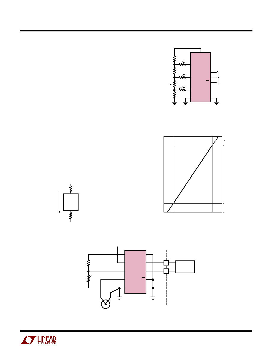
27
LTC2421/LTC2422
24212f
APPLICATIO S I FOR ATIO
W
U
U
U
resistance R
P1
in series with the half-bridge sensor are
removed by the FS
SET
input to the ADC. The absolute full-
scale output of the ADC (data out = FFFFF
HEX
) will occur
at V
IN
= V
B
= FS
SET
, see Figure 31. Similarly, the offset
errors due to R
P2
are removed by the ground sense input
ZS
SET
. The absolute zero output of the ADC (data out =
00000
HEX
) occurs at V
IN
= V
A
= ZS
SET
. Parasitic resistors
R
P3
to R
P5
have negligible errors due to the 1nA (typ)
leakage current at pins FS
SET
, ZS
SET
and V
IN
. The wide
dynamic input range (≠ 300mV to 5.3V) and low noise
(1.2ppm RMS) enable the LTC2421 or the LTC2422 to
directly digitize the output of the bridge sensor.
The LTC2422 is ideal for applications requiring continu-
ous monitoring of two input sensors. As shown in
Figure 32, the LTC2422 can monitor both a thermocouple
temperature probe and a cold junction temperature sen-
sor. Absolute temperature measurements can be
performed with a variety of thermocouples using digital
cold junction compensation.
Figure 31. Transfer Curve with Zero-Scale and Full-Scale Set
Figure 30. Half-Bridge Digitizer with
Zero-Scale and Full-Scale Sense
Figure 29. Errors Due to Excitation Currents
V
FULL-SCALE ERROR
SENSOR
SENSOR OUTPUT
R
P1
I
EXCITATION
+
≠
V
OFFSET ERROR
+
≠
+
≠
R
P2
24212 F29
V
CC
LTC2421
FS
SET
GND
SCK
V
IN
SDO
F
O
CS
ZS
SET
3-WIRE
SPI INTERFACE
1
9
8
7
10
24212 F03
2
3
5
R
P2
R
P5
I
DC
0
R
P1
V
B
V
A
6
R
P4
I
DC
0
I
EXCITATION
R
P3
I
DC
0
00000
H
12.5%
UNDER
RANGE
ADC DATA OUT
FFFFF
H
ZS
SET
FS
SET
V
IN
24212 F31
12.5%
EXTENDED
RANGE
Figure 32. Isolated Temperature Measurement
V
CC
F
O
FS
SET
ZS
SET
SCK
CH1
SDO
GND
CS
THERMOCOUPLE
COLD JUNCTION
ISOLATION
BARRIER
PROCESSOR
CH0
≠
+
1
10
12k
THERMISTOR
100
9
8
7
6
2
3
4
5
2.7V TO 5.5V
LTC2422
24212 F32
28
LTC2421/LTC2422
24212f
APPLICATIO S I FOR ATIO
W
U
U
U
The selection between CH0 and CH1 is automatic. Initially,
after power-up, a conversion is performed on CH0. For
each subsequent conversion, the input channel selection
is alternated. Embedded within the serial data output is a
status bit indicating which channel corresponds to the
conversion result. If the conversion was performed on
CH0, this bit (Bit 22) is LOW and is HIGH if the conversion
was performed on CH1 (see Figure 33).
There are no extra control or status pins required to per-
form the alternating 2-channel measurements. The
LTC2422 only requires two digital signals (SCK and SDO).
This simplification is ideal for isolated temperature mea-
surements or systems where minimal control signals are
available.
Pseudo Differential Applications
Generally, designers choose fully differential topologies
for several reasons. First, the interface to a 4- or 6-wire
bridge is simple (it is a differential output). Second, they
require good rejection of line frequency noise. Third, they
typically look at a small differential signal sitting on a
large common mode voltage; they need accurate
measurements of the differential signal independent of
the common mode input voltage. Many applications cur-
rently using fully differential analog-to-digital converters
for any of the above reasons may migrate to a pseudo
differential conversion using the LTC2422.
Direct Connection to a Full Bridge
The LTC2422 interfaces directly to a 4- or 6-wire bridge,
as shown in Figure 34. The LTC2422 includes a FS
SET
and
a ZS
SET
for sensing the excitation voltage directly across
the bridge. This eliminates errors due to excitation cur-
rents flowing through parasitic resistors. The LTC2422
also includes two single ended input channels which can
tie directly to the differential output of the bridge. The two
conversion results may be digitally subtracted yielding the
differential result.
The LTC2422's single ended rejection of line frequencies
(
±
2%) and harmonics is better than 110dB. Since the
device performs two independent single ended conver-
sions each with > 110dB rejection, the overall common
mode and differential rejection is much better than the
80dB rejection typically found in other differential input
delta-sigma converters.
In addition to excellent rejection of line frequency noise,
the LTC2422 also exhibits excellent single ended noise
rejection over a wide range of frequencies due to its 4
th
order sinc filter. Each single ended conversion indepen-
dently rejects high frequency noise (> 60Hz). Care must be
taken to insure noise at frequencies below 15Hz and at
multiples of the ADC sample rate (15,360Hz) are not
present. For this application, it is recommended the
LTC2422 is placed in close proximity to the bridge sensor
in order to reduce the noise injected into the ADC input. By
performing three successive conversions (CH0-CH1-CH0),
the drift and low frequency noise can be measured and
compensated for digitally.
Figure 33. Embedded Selected Channel Indicator
24212 F33
SCK
SDO
CH1
∑ ∑ ∑
∑ ∑ ∑
CH1 DATA OUT
CH0 DATA OUT
EOC
CH0
EOC
Figure 34. Pseudo Differential Strain Guage Application
V
CC
LTC2422
FS
SET
ZS
SET
SCK
CH1
SDO
F
O
CS
CH0
GND
3-WIRE
SPI INTERFACE
1
5V
9
8
7
10
6
24212 F32
2
350
350
350
350
3
4
5
I
DC
= 0
I
EXCITATION
I
DC
= 0
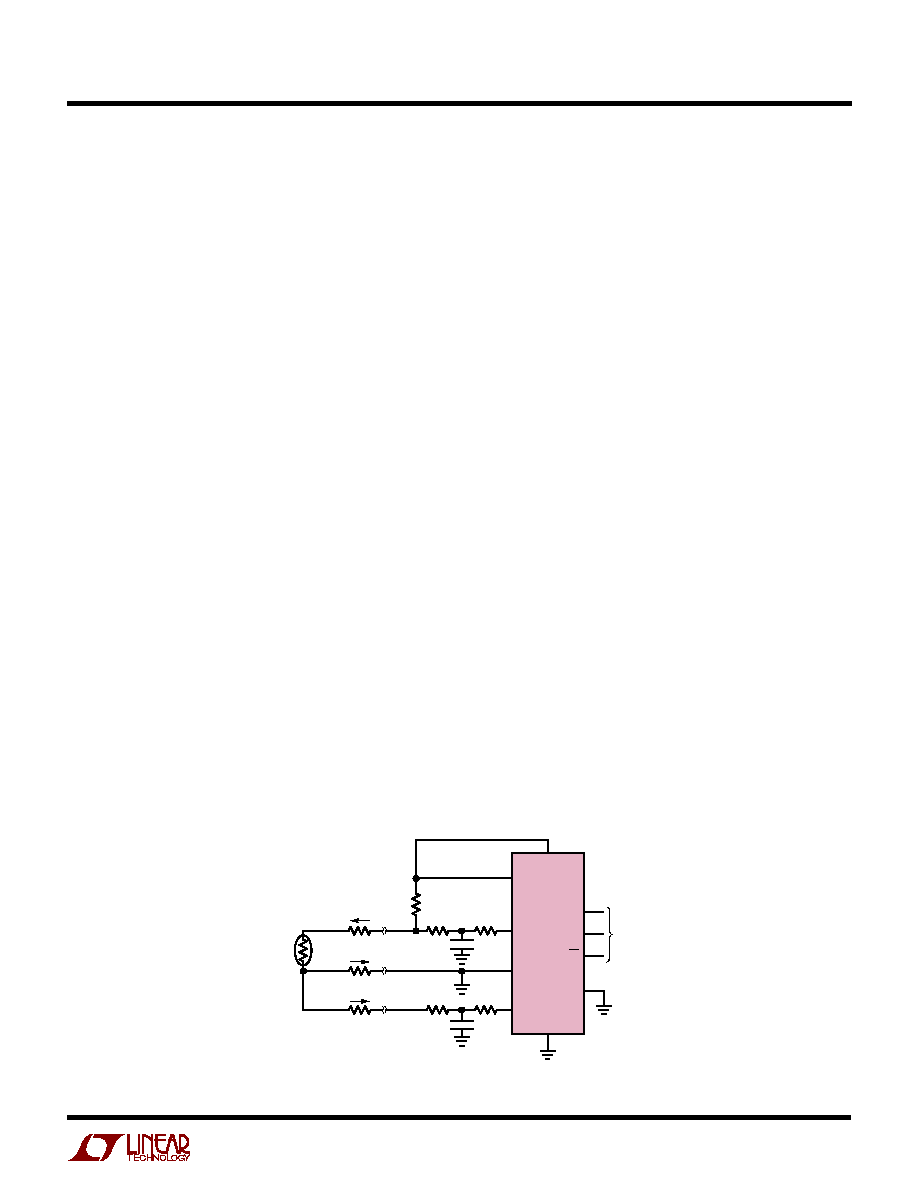
29
LTC2421/LTC2422
24212f
APPLICATIO S I FOR ATIO
W
U
U
U
The absolute accuracy (less than 10 ppm total error) of the
LTC2422 enables extremely accurate measurement of
small signals sitting on large voltages. Each of the two
pseudo differential measurements performed by the
LTC2422 is absolutely accurate independent of the com-
mon mode voltage output from the bridge. The pseudo
differential result obtained from digitally subtracting the
two single ended conversion results is accurate to within
the noise level of the device (3
µ
V
RMS
) times the square
root of 2, independent of the common mode input voltage.
Typically, a bridge sensor outputs 2mV/V full scale. With
a 5V excitation, this translates to a full-scale output of
10mV. Divided by the RMS noise of 8.4
µ
V(= 6
µ
V ∑ 1.414),
this circuit yields 1190 counts with no averaging or ampli-
fication. If more counts are required, several conversions
may be averaged (the number of effective counts is in-
creased by a factor of square root of 2 for each doubling
of averages).
An RTD Temperature Digitizer
RTDs used in remote temperature measurements often
have long lead lengths between the ADC and RTD sensor.
These long lead lengths lead to voltage drops due to exci-
tation current in the interconnect to the RTD. This voltage
drop can be measured and digitally removed using the
LTC2422 (see Figure 35).
The excitation current (typically 200
µ
A) flows from the
ADC through a long lead length to the remote temperature
sensor (RTD). This current is applied to the RTD, whose
resistance changes as a function of temperature (100
to
400
for 0
∞
C to 800
∞
C). The same excitation current flows
back to the ADC ground and generates another voltage
drop across the return leads. In order to get an accurate
measurement of the temperature, these voltage drops must
be measured and removed from the conversion result.
Assuming the resistance is approximately the same for the
forward and return paths (R1 = R2), the auxiliary channel
on the LTC2422 can measure this drop. These errors are
then removed with simple digital correction.
The result of the first conversion on CH0 corresponds to an
input voltage of V
RTD
+ R1 ∑ I
EXCITATION.
The result of the
second conversion (CH1) is ≠ R1 ∑ I
EXCITATION.
Note, the
LTC2422's input range is not limited to the supply rails, it
has underrange capabilities. The device's input range is
≠ 300mV to V
REF
+ 300mV. Adding the two conversion
results together, the voltage drop across the RTD's leads
are cancelled and the final result is V
RTD
.
An Isolated, 20-Bit Data Acquisition System
The LTC1535 is useful for signal isolation. Figure 36 shows
a fully isolated, 20-bit differential input A/D converter imple-
mented with the LTC1535 and LTC2422. Power on the
isolated side is regulated by an LT1761-5.0 low noise, low
dropout micropower regulator. Its output is suitable for
driving bridge circuits and for ratiometric applications.
During power-up, the LTC2422 becomes active at V
CC
=
2.3V, while the isolated side of the LTC1535 must wait for
V
CC2
to reach its undervoltage lockout threshold of 4.2V.
Figure 35. RTD Remote Temperature Measurement
V
CC
LTC2422
FS
SET
ZS
SET
SCK
CH0
SDO
F
O
CS
CH1
GND
3-WIRE
SPI INTERFACE
1
5V
9
8
7
10
6
24212 F35
2
4
3
+
≠
V
RTD
P
t
100
5
I
DC
= 0
I
EXCITATION
= 200
µ
A
I
EXCITATION
= 200
µ
A
R2
R1
5k
25
1000pF
5k
25
0.1
µ
F
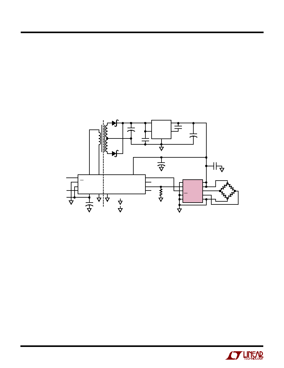
30
LTC2421/LTC2422
24212f
APPLICATIO S I FOR ATIO
W
U
U
U
+
+
F
O
SCK
SDO
CS
GND
V
CC
FS
SET
CH1
CH0
ZS
SET
LTC2422
24212 F36
LT1761-5
GND
10
µ
F
10V
TANT
10
µ
F
10V
TANT
+
10
µ
F
16V
TANT
+
10
µ
F
10V
TANT
10
µ
F
1
µ
F
T1
1/2 BAT54C
1/2 BAT54C
ISOLATION
BARRIER
= LOGIC COMMON
= FLOATING COMMON
T1 = COILTRONICS CTX02-14659
OR SIEMENS B78304-A1477-A3
1k
2
2
1
2
1
1
1
2
2
2
2
10
µ
F
CERAMIC
A
B
Y
Z
RO
RE
DE
DI
V
CC2
ST2
G1
V
CC1
G2
ST1
"SDO"
"SCK"
LOGIC 5V
IN
OUT
SHDN
BYP
LTC1535
Figure 36. Complete, Isolated 20-Bit Data Acquisition System
Below 4.2V, the LTC1535's driver outputs Y and Z are in a
high impedance state, allowing the 1k
pull-down to de-
fine the logic state at SCK. When the LTC2422 first be-
comes active, it samples SCK; a logic "0" provided by the
1k
pull-down invokes the external serial clock mode. In
this mode, the LTC2422 is controlled by a single clock line
from the nonisolated side of the barrier, through the
LTC1535's driver output Y. The entire power-up sequence,
from the time power is applied to V
CC1
until the LT1761's
output has reached 5V, is approximately 1ms.
Data returns to the nonisolated side through the LTC1535's
receiver at RO. An internal divider on receiver input B sets
a logic threshold of approximately 3.4V at input A, facili-
tating communications with the LTC2422's SDO output
without the need for any external components.
31
LTC2421/LTC2422
24212f
PACKAGE I FOR ATIO
U
U
W
Information furnished by Linear Technology Corporation is believed to be accurate and reliable.
However, no responsibility is assumed for its use. Linear Technology Corporation makes no represen-
tation that the interconnection of its circuits as described herein will not infringe on existing patent rights.
MS Package
10-Lead Plastic MSOP
(Reference LTC DWG # 05-08-1661)
MSOP (MS) 1001
0.53
±
0.01
(.021
±
.006)
SEATING
PLANE
0.18
(.007)
1.10
(.043)
MAX
0.17 ≠ 0.27
(.007 ≠ .011)
0.13
±
0.05
(.005
±
.002)
0.86
(.034)
REF
0.50
(.0197)
TYP
1 2 3 4 5
4.88
±
0.10
(.192
±
.004)
0.497
±
0.076
(.0196
±
.003)
REF
8
9
10
7 6
3.00
±
0.102
(.118
±
.004)
(NOTE 3)
3.00
±
0.102
(.118
±
.004)
NOTE 4
NOTE:
1. DIMENSIONS IN MILLIMETER/(INCH)
2. DRAWING NOT TO SCALE
3. DIMENSION DOES NOT INCLUDE MOLD FLASH, PROTRUSIONS OR GATE BURRS.
MOLD FLASH, PROTRUSIONS OR GATE BURRS SHALL NOT EXCEED 0.152mm (.006") PER SIDE
4. DIMENSION DOES NOT INCLUDE INTERLEAD FLASH OR PROTRUSIONS.
INTERLEAD FLASH OR PROTRUSIONS SHALL NOT EXCEED 0.152mm (.006") PER SIDE
5. LEAD COPLANARITY (BOTTOM OF LEADS AFTER FORMING) SHALL BE 0.102mm (.004") MAX
0.254
(.010)
0
∞
≠ 6
∞
TYP
DETAIL "A"
DETAIL "A"
GAUGE PLANE
5.23
(.206)
MIN
3.2 ≠ 3.45
(.126 ≠ .136)
0.889
±
0.127
(.035
±
.005)
RECOMMENDED SOLDER PAD LAYOUT
3.05
±
0.38
(.0120
±
.0015)
TYP
0.50
(.0197)
BSC
32
LTC2421/LTC2422
24212f
LT/TP 0202 2K ∑ PRINTED IN USA
©
LINEAR TECHNOLOGY CORPORATION 2002
RELATED PARTS
PART NUMBER
DESCRIPTION
COMMENTS
LT1019
Precision Bandgap Reference, 2.5V, 5V
3ppm/
∞
C Drift, 0.05% Max
LTC1050
Precision Chopper Stabilized Op Amp
No External Components 5
µ
V Offset, 1.6
µ
V
P-P
Noise
LT1236A-5
Precision Bandgap Reference, 5V
0.05% Max, 5ppm/
∞
C Drift
LTC1391
8-Channel Multiplexer
Low R
ON
: 45
, Low Charge Injection Serial Interface
LT1461-2.5
Precision Micropower Voltage Reference
50
µ
A Supply Current, 3ppm/
∞
C Drift
LTC1535
Isolated RS485 Transceiver
2500V
RMS
Isolation
LTC2400
24-Bit, No Latency
ADC in SO-8
4ppm INL, 10ppm Total Unadjusted Error, 200
µ
A
LTC2401/LTC2402
1-/2-Channel, 24-Bit, No Latency
ADC in MSOP
0.6ppm Noise, 4ppm INL, Pin Compatible with the LTC2421/LTC2422
LTC2404/LTC2408
4-/8-Channel, 24-Bit, No Latency
ADC
4ppm INL, 10ppm Total Unadjusted Error, 200
µ
A
LTC2413
24-Bit, No Latency
ADC
Simultaneous 50Hz and 60Hz Rejection, 0.16ppm Noise
LTC2415
24-Bit, Fully Differential, No Latency
ADC
15Hz Output Rate at 60Hz Rejection, Pin Conpatible with the LTC2410
LTC2420
20-Bit, No Latency
ADC in SO-8
1.2ppm Noise, 8ppm INL, Pin Compatible with LTC2400
LTC2424/LTC2428
4-/8-Channel, 20-Bit, No Latency
ADC
1.2ppm Noise, 8ppm INL, Pin Compatible with LTC2404/LTC2408
LTC2430
20-Bit, Fully Differential, No Latency
ADC in SSOP-16
0.16ppm Noise, 2ppm INL, 10ppm Total Unadjusted Error, 200
µ
A
LTC2431
24-Bit, Fully Differential, No Latency
ADC in MS10
0.29ppm Noise, 4ppm INL, 10ppm Total Unadjusted Error, 200
µ
A
Linear Technology Corporation
1630 McCarthy Blvd., Milpitas, CA 95035-7417
(408) 432-1900
q
FAX: (408) 434-0507
q
www.linear.com
TYPICAL APPLICATIO
U
Figure 37 shows the block diagram of a demo circuit
(contact LTC for a demonstration) of a multichannel
isolated temperature measurement system. This circuit
decodes an address to select which LTC2422 receives a
24-bit burst of SCK signal. All devices independently
convert either the thermal couple output or the thermistor
cold junction output. After each conversion, the devices
enter their sleep state and wait for the SCK signal before
clocking out data and beginning the next conversion.
V
CC
FS
SET
CH1
SDO
SCK
CH0
ZS
SET
LTC2422
A
Y
D1
RE
R0
LTC1535
V
CC
FS
SET
CH1
SDO
SCK
CH0
2500V
ZS
SET
LTC2422
A
Y
D1
RE
R0
LTC1535
V
CC
FS
SET
CH1
SDO
SCK
24212 F37
CH0
ZS
SET
LTC2422
A
Y
D1
HC138
HC595
ADDRESS
LATCH
RE
R0
LTC1535
SEE FIGURE 34 FOR
THE COMPLETE CIRCUIT
HC138
SCK
SD0
D
IN
(ADDRESS
OR COUNTER)
+
≠
Figure 37. Mulitchannel Isolated Temperature Measurement System