2600f.pm6
1
LTC2600/LTC2610/LTC2620
2600f
Octal 16-/14-/12-Bit
Rail-to-Rail DACs in 16-Lead SSOP
The LTC
®
2600/LTC2610/LTC2620 are octal 16-, 14- and
12-bit, 2.5V-to-5.5V rail-to-rail voltage-output DACs in
16-lead narrow SSOP packages. They have built-in high
performance output buffers and are guaranteed mono-
tonic.
These parts establish new board-density benchmarks for
16- and 14-bit DACs and advance performance standards
for output drive, crosstalk and load regulation in single-
supply, voltage-output multiples.
The parts use a simple SPI/MICROWIRE
TM
compatible
3-wire serial interface which can be operated at clock rates
up to 50MHz. Daisy-chain capability and a hardware CLR
function are included.
The LTC2600/LTC2610/LTC2620 incorporate a power-on
reset circuit. During power-up, the voltage outputs rise
less than 10mV above zero scale; and after power-up, they
stay at zero scale until a valid write and update take place.
s
Smallest Pin Compatible Octal DACs:
LTC2600: 16 Bits
LTC2610: 14 Bits
LTC2620: 12 Bits
s
Guaranteed 16-Bit Monotonic Over Temperature
s
Tiny 16-Lead Narrow SSOP Package
s
Wide 2.5V to 5.5V Supply Range
s
Low Power Operation: 250
µ
A per DAC at 3V
s
Individual Channel Power-Down to 1
µ
A, Max
s
Ultralow Crosstalk between DACs (<10
µ
V)
s
High Rail-to-Rail Output Drive (
±
15mA, Min)
s
Double-Buffered Digital Inputs
s
Pin-Compatible 10-/8-Bit Versions
(LTC1660/LTC1665)
s
Mobile Communications
s
Process Control and Industrial Automation
s
Instrumentation
s
Automatic Test Equipment
Differential Nonlinearity (LTC2600)
, LTC and LT are registered trademarks of Linear Technology Corporation.
2
15
1
GND
V
OUT A
V
OUT B
V
OUT C
V
OUT D
REF
CS/LD
SCK
V
CC
V
OUT H
V
OUT G
V
OUT F
V
OUT E
CLR
SDO
SDI
2600 BD
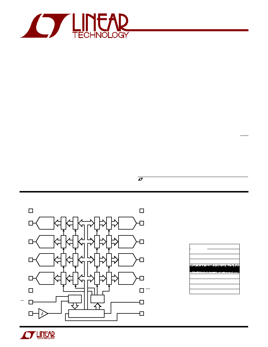
16
DAC A
3
14
4
13
5
7
6
8
10
11
9
12
DECODE
CONTROL
LOGIC
32-BIT SHIFT REGISTER
REGISTER
REGISTER
DAC H
REGISTER
REGISTER
DAC B
REGISTER
REGISTER
DAC G
REGISTER
REGISTER
DAC C
REGISTER
REGISTER
DAC F
REGISTER
REGISTER
DAC D
REGISTER
REGISTER
DAC E
REGISTER
REGISTER
CODE
0
16384
32768
49152
65535
DNL (LSB)
2600 G21
1.0
0.8
0.6
0.4
0.2
0
0.2
0.4
0.6
0.8
1.0
V
CC
= 5V
V
REF
= 4.096V
MICROWIRE is a trademark of National Semiconductor Corporation.
APPLICATIO S
U
FEATURES
DESCRIPTIO
U
BLOCK DIAGRA
W
2
LTC2600/LTC2610/LTC2620
2600f
A
U
G
W
A
W
U
W
A
R
BSOLUTE
XI
TI
S
ORDER PART
NUMBER
W
U
U
PACKAGE/ORDER I FOR ATIO
T
JMAX
= 125
°
C,
JA
= 150
°
C/W
(Note 1)
Any Pin to GND ........................................... 0.3V to 6V
Any Pin to V
CC
............................................. 6V to 0.3V
Maximum Junction Temperature ......................... 125
°
C
Operating Temperature Range
LTC2600C/LTC2610C/LTC2620C .......... 0
°
C to 70
°
C
LTC2600I/LTC2610I/LTC2620I .......... 40
°
C to 85
°
C
Storage Temperature Range ................ 65
°
C to 150
°
C
Lead Temperature (Soldering, 10 sec)................ 300
°
C
GN PART MARKING
ELECTRICAL C
C
HARA TERISTICS
The
q
denotes specifications which apply over the full operating
temperature range, otherwise specifications are at T
A
= 25
°
C. V
CC
= 2.5V to 5.5V, V
REF
V
CC
, V
OUT
unloaded, unless otherwise noted.
1
2
3
4
5
6
7
8
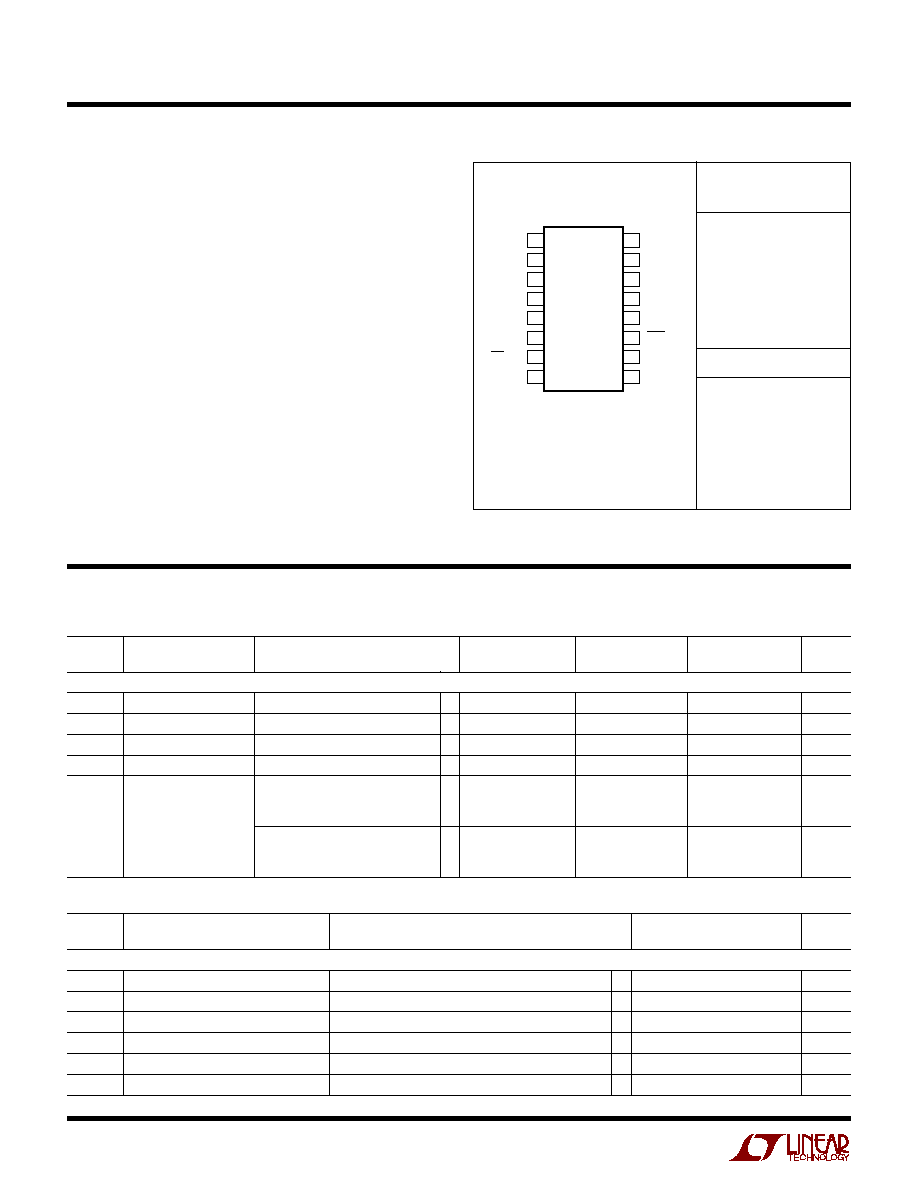
TOP VIEW
GN PACKAGE
16-LEAD PLASTIC SSOP
16
15
14
13
12
11
10
9
GND
V
OUT A
V
OUT B
V
OUT C
V
OUT D
REF
CS/LD
SCK
V
CC
V
OUT H
V
OUT G
V
OUT F
V
OUT E
CLR
SDO
SDI
LTC2600CGN
LTC2600IGN
LTC2610CGN
LTC2610IGN
LTC2620CGN
LTC2620IGN
2600
2600I
2610
2610I
2620
2620I
Consult LTC Marketing for parts specified with wider operating temperature ranges.
LTC2600/LTC2610/LTC2620
SYMBOL
PARAMETER
CONDITIONS
MIN
TYP
MAX
UNITS
DC Performance
ZSE
Zero-Scale Error
V
CC
= 5V, V
REF
= 4.096V Code = 0
q
1
9
mV
V
OS
Offset Error
V
CC
= 5V, V
REF
= 4.096V, (Note 7)
q
±
1
±
9
mV
V
OS
Temperature Coefficient
1.7
µ
V/
°
C
GE
Gain Error
V
CC
= 5V, V
REF
= 4.096V
q
±
0.2
±
0.7
%FSR
Gain Temperature Coefficient
6.5
ppm/
°
C
PSR
Power Supply Rejection
V
CC
=
±
10%
80
dB
LTC2620
LTC2610
LTC2600
SYMBOL
PARAMETER
CONDITONS
MIN
TYP
MAX
MIN
TYP
MAX
MIN
TYP
MAX
UNITS
DC Performance
Resolution
q
12
14
16
Bits
Monotonicity
V
CC
= 5V, V
REF
= 4.096V (Note 2)
q
12
14
16
Bits
DNL
Differential Nonlinearity
V
CC
= 5V, V
REF
= 4.096V (Note 2)
q
±
0.5
±
1
±
1
LSB
INL
Integral Nonlinearity
V
CC
= 5V, V
REF
= 4.096V (Note 2)
q
±
0.75
±
4
±
3
±
16
±
12
±
64
LSB
Load Regulation
V
REF
= V
CC
= 5V, Midscale
I
OUT
= 0mA to 15mA Sourcing
q
0.025 0.125
0.1
0.5
0.3
2
LSB/mA
I
OUT
= 0mA to 15mA Sinking
q
0.025 0.125
0.1
0.5
0.3
2
LSB/mA
V
REF
= V
CC
= 2.5V, Midscale
I
OUT
= 0mA to 7.5mA Sourcing
q
0.05
0.25
0.2
1
0.8
4
LSB/mA
I
OUT
= 0mA to 7.5mA Sinking
q
0.05
0.25
0.2
1
0.8
4
LSB/mA
3
LTC2600/LTC2610/LTC2620
2600f
ELECTRICAL C
C
HARA TERISTICS
The
q
denotes specifications which apply over the full operating
temperature range, otherwise specifications are at T
A
= 25
°
C. V
CC
= 2.5V to 5.5V, V
REF
V
CC
, V
OUT
unloaded, unless otherwise noted.
LTC2600/LTC2610/LTC2620
SYMBOL
PARAMETER
CONDITIONS
MIN
TYP
MAX
UNITS
R
OUT
DC Output Impedance
V
REF
= V
CC
= 5V, Midscale; 15mA
I
OUT
15mA
q
0.025
0.15
V
REF
= V
CC
= 2.5V, Midscale; 7.5mA
I
OUT
7.5mA
q
0.030
0.15
DC Crosstalk (Note 4)
Due to Full Scale Output Change (Note 5)
10
µ
V
Due to Load Current Change
3.5
µ
V/mA
Due to Powering Down (per Channel)
7.3
µ
V
I
SC
Short-Circuit Output Current
V
CC
= 5.5V, V
REF
= 5.6V
Code: Zero Scale; Forcing Output to V
CC
q
15
34
60
mA
Code: Full Scale; Forcing Output to GND
q
15
34
60
mA
V
CC
= 2.5V, V
REF
= 2.6V
Code: Zero Scale; Forcing Output to V
CC
q
7.5
18
50
mA
Code: Full Scale; Forcing Output to GND
q
7.5
24
50
mA
Reference Input
Input Voltage Range
q
0
V
CC
V
Resistance
Normal Mode
q
11
16
20
k
Capacitance
90
pF
I
REF
Reference Current, Power Down Mode
All DACs Powered Down
q
0.001
1
µ
A
Power Supply
V
CC
Positive Supply Voltage
For Specified Performance
q
2.5
5.5
V
I
CC
Supply Current
V
CC
= 5V (Note 3)
q
2.6
4
mA
V
CC
= 3V (Note 3)
q
2.0
3.2
mA
All DACs Powered Down (Note 3) V
CC
= 5V
q
0.35
1
µ
A
All DACs Powered Down (Note 3) V
CC
= 3V
q
0.10
1
µ
A
AC Performance
Voltage Output Slew Rate
0.80
V/
µ
s
Capacitive Load Driving
1000
pF
Glitch Impulse
At Midscale Transition
12
nV · s
Multiplying Bandwidth
180
kHz
e
n
Output Voltage Noise Density
At f = 1kHz
120
nV/
Hz
At f = 10kHz
100
nV/
Hz
Output Voltage Noise
0.1Hz to 10Hz
15
µ
V
P-P
Digital I/O
V
IH
Digital Input High Voltage
V
CC
= 2.5V to 5.5V
q
2.4
V
V
CC
= 2.5V to 3.6V
q
2.0
V
V
IL
Digital Input Low Voltage
V
CC
= 4.5V to 5.5V
q
0.8
V
V
CC
= 2.7V to 5.5V
q
0.6
V
V
CC
= 2.5V to 5.5V
q
0.5
V
V
OH
Digital Output High Voltage
Load Current = 100
µ
A
q
V
CC
0.4
V
V
OL
Digital Output Low Voltage
Load Current = +100
µ
A
q
0.4
V
I
LK
Digital Input Leakage
V
IN
= GND to V
CC
q
±
1
µ
A
C
IN
Digital Input Capacitance
(Note 6)
q
8
pF
4
LTC2600/LTC2610/LTC2620
2600f
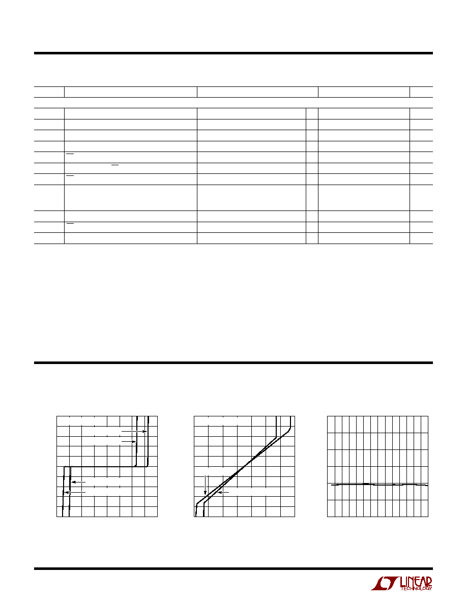
Current Limiting
Load Regulation
Offset Error vs Temperature
TI I G CHARACTERISTICS
U
W
The
q
denotes specifications which apply over the full operating temperature
range, otherwise specifications are at T
A
= 25
°
C. (See Figure 1) (Note 6)
Note 1: Absolute maximum ratings are those values beyond which the life
of a device may be impaired.
Note 2: Linearity and monotonicity are defined from code k
L
to code
2
N
1, where N is the resolution and k
L
is given by k
L
= 0.016(2
N
/V
REF
),
rounded to the nearest whole code. For V
REF
= 4.096V and N = 16, k
L
=
256 and linearity is defined from code 256 to code 65,535.
SYMBOL
PARAMETER
CONDITONS
MIN
TYP
MAX
UNITS
V
CC
= 2.5V to 5.5V
t
1
SDI Valid to SCK Setup
q
4
ns
t
2
SDI Valid to SCK Hold
q
4
ns
t
3
SCK High Time
q
9
ns
t
4
SCK Low Time
q
9
ns
t
5
CS/LD Pulse Width
q
10
ns
t
6
LSB SCK High to CS/LD High
q
7
ns
t
7
CS/LD Low to SCK High
q
7
ns
t
8
SDO Propagation Delay from SCK Falling Edge
C
LOAD
= 10pF
V
CC
= 4.5V to 5.5V
q
20
ns
V
CC
= 2.5V to 5.5V
q
45
ns
t
9
CLR Pulse Width
q
20
ns
t
10
CS/LD High to SCK Positive Edge
q
7
ns
SCK Frequency
50% Duty Cycle
q
50
MHz
Note 3: Digital inputs at 0V or V
CC
.
Note 4: DC crosstalk is measured with V
CC
= 5V and V
REF
= 4.096V, with
the measured DAC at midscale, unless otherwise noted.
Note 5: R
L
= 2k
to GND or V
CC
.
Note 6: Guaranteed by design and not production tested.
Note 7: Inferred from measurement at code 256 (LTC2600), code 64
(LTC2610) or code 16 (LTC2620).
TEMPERATURE (
°
C)
50
30
10
10
30
50
70
90
OFFSET ERROR (mV)
2600 G03
3
2
1
0
1
2
3
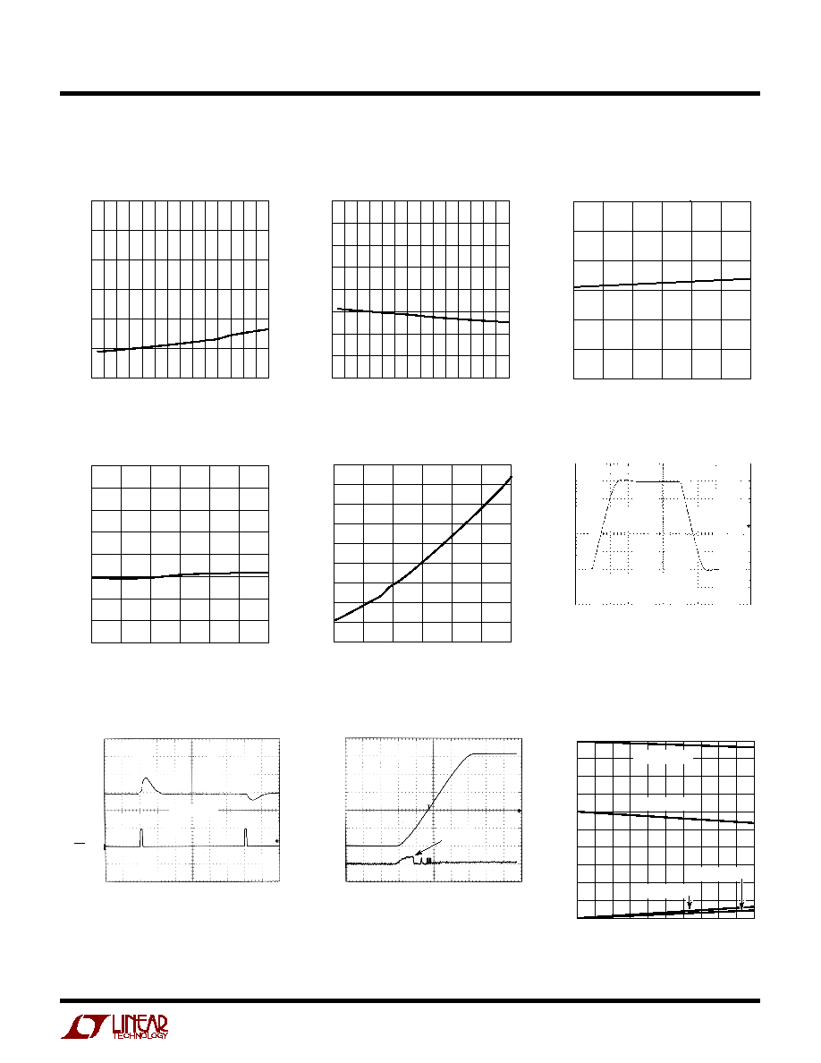
TYPICAL PERFOR A CE CHARACTERISTICS
U
W
(LTC2600/LTC2610/LTC2620)
I
OUT
(mA)
40 30 20 10
0
10
20
30
40
V
OUT
(V)
2600 G01
0.10
0.08
0.06
0.04
0.02
0
0.02
0.04
0.06
0.08
0.10
V
REF
= V
CC
= 5V
V
REF
= V
CC
= 3V
V
REF
= V
CC
= 5V
V
REF
= V
CC
= 3V
CODE = MIDSCALE
I
OUT
(mA)
35
25
15
5
5
15
25
35
V
OUT
(mV)
2600 G02
1.0
0.8
0.6
0.4
0.2
0
0.2
0.4
0.6
0.8
1.0
V
REF
= V
CC
= 5V
CODE = MIDSCALE
V
REF
= V
CC
= 3V
5
LTC2600/LTC2610/LTC2620
2600f
TYPICAL PERFOR A CE CHARACTERISTICS
U
W
Gain Error vs Temperature
Offset Error vs V
CC
TEMPERATURE (
°
C)
50
30
10
10
30
50
70
90
GAIN ERROR (%FSR)
2600 G05
0.4
0.3
0.2
0.1
0
0.1
0.2
0.3
0.4
TEMPERATURE (
°
C)
50
30
10
10
30
50
70
90
ZERO-SCALE ERROR (mV)
2600 G04
3
2.5
2.0
1.5
1.0
0.5
0
Zero-Scale Error vs Temperature
V
CC
(V)
2.5
3
3.5
4
4.5
5
5.5
OFFSET ERROR (mV)
2600 G06
3
2
1
0
1
2
3
V
CC
(V)
2.5
3
3.5
4
4.5
5
5.5
GAIN ERROR (%FSR)
2600 G07
0.4
0.3
0.2
0.1
0
0.1
0.2
0.3
0.4
V
CC
(V)
2.5
3
3.5
4
4.5
5
5.5
I
CC
(nA)
2600 G08
450
400
350
300
250
200
150
100
50
0
2.5
µ
s/DIV
V
OUT
0.5V/DIV
2600 G09
V
REF
= V
CC
= 5V
1/4-SCALE TO 3/4-SCALE
I
CC
Shutdown vs V
CC
Large-Signal Settling
Gain Error vs V
CC
LTC2600/LTC2610/LTC2620
Midscale Glitch Impulse
Power-On Reset Glitch
Headroom at Rails vs Output
Current
V
OUT
10mV/DIV
CS/LD
5V/DIV
2.5
µ
s/DIV
2600 G10
12nV-s TYP
V
OUT
10mV/DIV
250
µ
s/DIV
2600 G11
V
CC
1V/DIV
4mV PEAK
4mV PEAK
I
OUT
(mA)
0
1
2
3
4
5
6
7
8
9
10
V
OUT
(V)
2600 G12
5.0
4.5
4.0
3.5
3.0
2.5
2.0
1.5
1.0
0.5
0
5V SOURCING
3V SOURCING
3V SINKING
5V SINKING