 | ÐлекÑÑоннÑй компоненÑ: LTC2845CG | СкаÑаÑÑ:  PDF PDF  ZIP ZIP |
2845i.pm6
1
LTC2845
2845i
3.3V Software-Selectable
Multiprotocol Transceiver
April 2002
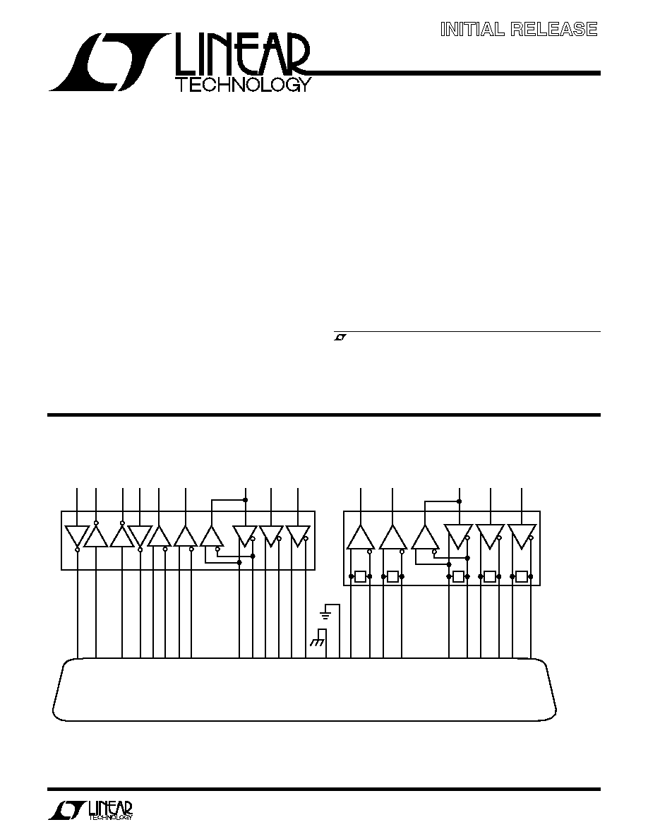
D2
D1
LTC2845
RTS
DTR
DSR
DCD
CTS
D3
R2
R1
R3
LL
RI
TM
RL
TXD
SCTE
TXC
RXC
RXD
2
14
24
11
15
12
17
9
3
1
4
19
20
6
23
22
5
13
8
10
18
*
21
25
7
16
D4
D5
R4
R5
LTC2846
D1
D2
D3
R1
R2
R3
T
T
T
T
T
*OPTIONAL
2845 TA01
RTS A (105)
RTS B
DTR A (108)
DTR B
CTS A (106)
SG (102)
SHIELD (101)
DB-25 CONNECTOR
DCD A (107)
DCD B
DSR A (109)
DSR B
LL A (141)
RI A (125)
TM A (142)
RL A (140)
CTS B
SCTE B
SCTE A (113)
TXD B
TXD A (103)
TXC A (114)
TXC B
RXC A (115)
RXC B
RXD A (104)
RXD B
DTE or DCE Multiprotocol Serial Interface with DB-25 Connector
, LTC and LT are registered trademarks of Linear Technology Corporation.
s
Data Networking
s
CSU and DSU
s
Data Routers
s
Software-Selectable Transceiver Supports:
RS232, RS449, EIA530, EIA530-A, V.35, V.36, X.21
s
Operates from Single 3.3V Supply with LTC2846
s
Complete DTE or DCE Port with LTC2846
The LTC
®
2845 is a 5-driver/5-receiver multiprotocol trans-
ceiver. The LTC2845 and LTC2846 form the core of a
complete software-selectable DTE or DCE interface port that
supports the RS232, RS449, EIA530, EIA530-A, V.35, V.36
or X.21 protocols.
The LTC2845 operates from a 3.3V supply and supplies
provided by the LTC2846. This part is available in a 36-lead
SSOP surface mount package.
APPLICATIO S
U
FEATURES
DESCRIPTIO
U
TYPICAL APPLICATIO
U
Final Electrical Specifications
Information furnished by Linear Technology Corporation is believed to be accurate and reliable.
However, no responsibility is assumed for its use. Linear Technology Corporation makes no represen-
tation that the interconnection of its circuits as described herein will not infringe on existing patent rights.
2
LTC2845
2845i
ABSOLUTE
M
AXI
M
U
M
RATINGS
W
W
W
U
PACKAGE/ORDER I
N
FOR
M
ATIO
N
W
U
U
ORDER PART
NUMBER
(Note 1)
Supply Voltage
V
CC
....................................................... 0.3V to 6.5V
V
IN .....................................................................
0.3V to 6.5V
V
EE ......................................................................
10V to 0.3V
V
DD .....................................................................
0.3V to 10V
Input Voltage
Transmitters ........................... 0.3V to (V
CC
+ 0.3V)
Receivers ............................................... 18V to 18V
Logic Pins .............................. 0.3V to (V
CC
+ 0.3V)
Output Voltage
Transmitters .................. (V
EE
0.3V) to (V
DD
+ 0.3V)
Receivers ................................. 0.3V to (V
IN
+ 0.3V)
Short-Circuit Duration
Transmitter Output ..................................... Indefinite
Receiver Output .......................................... Indefinite
V
EE
.................................................................. 30 sec
Operating Temperature Range
LTC2845CG ............................................. 0
°
C to 70
°
C
LTC2845IG ........................................ 40
°
C to 85
°
C
Storage Temperature Range ................ 65
°
C to 150
°
C
Lead Temperature (Soldering, 10 sec)................. 300
°
C
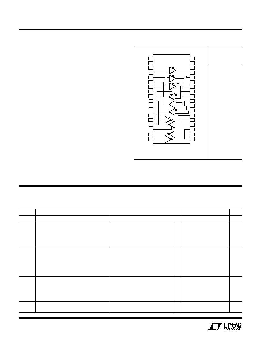
LTC2845CG
LTC2845IG
1
2
3
4
5
6
7
8
9
10
11
12
13
14
15
16
17
18
TOP VIEW
36
35
34
33
32
31
30
29
28
27
26
25
24
23
22
21
20
19
V
CC
V
DD
D1
D2
D3
R1
R2
R3
D4
R4
M0
M1
M2
DCE/DTE
D4ENB
R4EN
R5
D5
V
EE
GND
D1 A
D1 B
D2 A
D2 B
D3/R1 A
D3/R1 B
R2 A
R2 B
R3 A
R3 B
D4 A
R4 A
R5 A
D5 A
V
IN
V
CC
R1
D2
D1
D3
R3
G PACKAGE
36-LEAD PLASTIC SSOP
D5
R5
D4
R2
R4
T
JMAX
= 125
°
C,
JA
= 90
°
C/ W,
JC
= 35
°
C/ W
Consult LTC Marketing for parts specified with wider operating temperature ranges.
The
q
denotes specifications which apply over the full operating tempera-
ture range, otherwise specifications are at T
A
= 25
°
C. V
CC
= 5V, V
IN
= 3.3V, V
DD
= 8V, V
EE
= 7V for V.28, 5.5V for V.10, V.11
(Notes 2, 3)
ELECTRICAL CHARACTERISTICS
SYMBOL
PARAMETER
CONDITIONS
MIN
TYP
MAX
UNITS
Supplies
I
CC
V
CC
Supply Current (DCE Mode,
RS530, RS530-A, X.21 Modes, No Load
2.7
mA
All Digital Pins = GND or V
IN
)
RS530, RS530-A, X.21 Modes, Full Load
q
110
150
mA
V.28 Mode, No Load
q
1
3
mA
V.28 Mode, Full Load
q
1
3
mA
No-Cable Mode
q
700
1400
µ
A
I
EE
V
EE
Supply Current (DCE Mode,
RS530, RS530-A, X.21 Modes, No Load
2
mA
All Digital Pins = GND or V
IN
)
RS530, X.21 Modes, Full Load
23
mA
RS530-A, Full Load
34
mA
V.28 Mode, No Load
1
mA
V.28 Mode, Full Load
12
mA
No-Cable Mode
10
µ
A
I
DD
V
DD
Supply Current (DCE Mode,
RS530, RS530-A, X.21 Modes, No Load
0.3
mA
All Digital Pins = GND or V
IN
)
RS530, RS530-A, X.21 Modes, Full Load
0.3
mA
V.28 Mode, No Load
1
mA
V.28 Mode, Full Load
13.5
mA
No-Cable Mode
10
µ
A
I
VIN
V
IN
Supply Current (DCE Mode,
All Modes Except No-Cable Mode
650
µ
A
All Digital Pins = GND or V
IN
)
3
LTC2845
2845i
The
q
denotes specifications which apply over the full operating tempera-
ture range, otherwise specifications are at T
A
= 25
°
C. V
CC
= 5V, V
IN
= 3.3V, V
DD
= 8V, V
EE
= 7V for V.28, 5.5V for V.10, V.11
(Notes 2, 3)
ELECTRICAL CHARACTERISTICS
SYMBOL
PARAMETER
CONDITIONS
MIN
TYP
MAX
UNITS
P
D
Internal Power Dissipation (DCE Mode,
RS530, RS530-A, X.21 Modes, Full Load
340
mW
All Digital Pins = GND or V
IN
)
V.28 Mode, Full Load
64
mW
Logic Inputs and Outputs
V
IH
Logic Input High Voltage
q
2
V
V
IL
Logic Input Low Voltage
V
CC
= 5V
q
0.8
V
R4EN when V
CC
= 3.3V
0.5
V
I
IN
Logic Input Current
D1, D2, D3, D4, D5
q
±
10
µ
A
M0, M1, M2, DCE, D4ENB, R4EN = GND
q
30
75
120
µ
A
M0, M1, M2, DCE, D4ENB, R4EN = V
IN
q
±
10
µ
A
V
OH
Output High Voltage
I
O
= 3mA
q
2.7
3
V
V
OL
Output Low Voltage
I
O
= 1.6mA
q
0.2
0.4
V
I
OSR
Output Short-Circuit Current
0V
V
O
V
IN
q
±
50
mA
I
OZR
Three-State Output Current
M0 = M1 = M2 = V
IN
, V
O
= GND
q
30
85
160
µ
A
M0 = M1 = M2 = V
IN
, V
O
= V
IN
q
±
10
µ
A
V.11 Driver
V
ODO
Open Circuit Differential Output Voltage
R
L
= 1.95k (Figure 1)
q
±
5
V
V
ODL
Loaded Differential Output Voltage
R
L
= 50
(Figure 1)
0.5V
ODO
0.67V
ODO
V
q
±
2
V
V
OD
Change in Magnitude of Differential
R
L
= 50
(Figure 1)
q
0.2
V
Output Voltage
V
OC
Common Mode Output Voltage
R
L
= 50
(Figure 1)
q
3
V
V
OC
Change in Magnitude of Common Mode
R
L
= 50
(Figure 1)
q
0.2
V
Output Voltage
I
SS
Short-Circuit Current
V
OUT
= GND
±
150
mA
I
OZ
Output Leakage Current
0.25V
V
O
0.25V, Power Off or
q
±
1
±
100
µ
A
No-Cable Mode or Driver Disabled
t
r
, t
f
Rise or Fall Time
LTC2845C (Figures 2, 5)
q
2
15
25
ns
LTC2845I (Figures 2, 5)
q
2
15
35
ns
t
PLH
Input to Output
LTC2845C (Figures 2, 5)
q
20
40
65
ns
LTC28451 (Figures 2, 5)
q
20
40
75
ns
t
PHL
Input to Output
LTC2845C (Figures 2, 5)
q
20
40
65
ns
LTC2845I (Figures 2, 5)
q
20
40
75
ns
t
Input to Output Difference,
t
PLH
t
PHL
LTC2845C (Figures 2, 5)
q
0
3
12
ns
LTC2845I (Figures 2, 5)
q
0
3
17
ns
t
SKEW
Output to Output Skew
(Figures 2, 5)
3
ns
V.11 Receiver
V
TH
Input Threshold Voltage
7V
V
CM
7V
q
0.2
0.2
V
V
TH
Input Hysteresis
7V
V
CM
7V
q
15
40
mV
I
IN
Input Current (A, B)
10V
V
A,B
10V
q
±
0.66
mA
R
IN
Input Impedance
10V
V
A,B
10V
q
15
30
k
t
r
, t
f
Rise or Fall Time
(Figures 2, 6)
15
ns
4
LTC2845
2845i
The
q
denotes specifications which apply over the full operating tempera-
ture range, otherwise specifications are at T
A
= 25
°
C. V
CC
= 5V, V
IN
= 3.3V, V
DD
= 8V, V
EE
= 7V for V.28, 5.5V for V.10, V.11
(Notes 2, 3)
ELECTRICAL CHARACTERISTICS
SYMBOL
PARAMETER
CONDITIONS
MIN
TYP
MAX
UNITS
t
PLH
Input to Output
LTC2845C C
L
= 50pF (Figures 2, 6)
q
50
80
ns
LTC2845I C
L
= 50pF (Figures 2, 6)
q
50
90
ns
t
PHL
Input to Output
LTC2845C C
L
= 50pF (Figures 2, 6)
q
50
80
ns
LTC2845I C
L
= 50pF (Figures 2, 6)
q
50
90
ns
t
Input to Output Difference,
t
PLH
t
PHL
LTC2845C C
L
= 50pF (Figures 2, 6)
q
0
4
16
ns
LTC2845I C
L
= 50pF (Figures 2, 6)
q
0
4
21
ns
V.10 Driver
V
O
Output Voltage
Open Circuit, R
L
= 3.9k
q
±
4
±
6
V
V
T
Output Voltage
R
L
= 450
(Figure 3)
q
±
3.6
V
R
L
= 450
(Figure 3)
0.9V
O
I
SS
Short-Circuit Current
V
O
= GND
±
150
mA
I
OZ
Output Leakage Current
0.25V
V
O
0.25V, Power Off or
q
±
0.1
±
100
µ
A
No-Cable Mode or Driver Disabled
t
r
, t
f
Rise or Fall Time
R
L
= 450
, C
L
= 100pF (Figures 3, 7)
2
µ
s
t
PLH
Input to Output
R
L
= 450
, C
L
= 100pF (Figures 3, 7)
1
µ
s
t
PHL
Input to Output
R
L
= 450
, C
L
= 100pF (Figures 3, 7)
1
µ
s
V.10 Receiver
V
TH
Receiver Input Threshold Voltage
q
0.25
0.25
V
V
TH
Receiver Input Hysteresis
q
25
50
mV
I
IN
Receiver Input Current
10V
V
A
10V
q
±
0.66
mA
R
IN
Receiver Input Impedance
10V
V
A
10V
q
15
30
k
t
r
, t
f
Rise or Fall Time
C
L
= 50pF (Figures 4, 8)
15
ns
t
PLH
Input to Output
C
L
= 50pF (Figures 4, 8)
55
ns
t
PHL
Input to Output
C
L
= 50pF (Figures 4, 8)
109
ns
t
Input to Output Difference,
t
PLH
t
PHL
C
L
= 50pF (Figures 4, 8)
60
ns
V.28 Driver
V
O
Output Voltage
Open Circuit
q
±
10
V
R
L
= 3k (Figure 3)
q
±
5
±
8.5
V
I
SS
Short-Circuit Current
V
O
= GND
q
±
150
mA
I
OZ
Output Leakage Current
0.25V
V
O
0.25V, Power Off or
q
±
1
±
100
µ
A
No-Cable Mode or Driver Disabled
SR
Slew Rate
R
L
= 3k, C
L
= 2500pF (Figures 3, 7)
q
4
30
V/
µ
s
t
PLH
Input to Output
R
L
= 3k, C
L
= 2500pF (Figures 3, 7)
q
1.3
2.5
µ
s
t
PHL
Input to Output
R
L
= 3k, C
L
= 2500pF (Figures 3, 7)
q
1.3
2.5
µ
s
V.28 Receiver
V
THL
Input Low Threshold Voltage
q
0.8
V
V
TLH
Input High Threshold Voltage
q
2
V
V
TH
Receiver Input Hysterisis
q
0.1
0.3
V
R
IN
Receiver Input Impedance
15V
V
A
15V
q
3
5
7
k
t
r
, t
f
Rise or Fall Time
C
L
= 50pF (Figures 4, 8)
15
ns
t
PLH
Input to Output
C
L
= 50pF (Figures 4, 8)
q
60
100
ns
t
PHL
Input to Output
C
L
= 50pF (Figures 4, 8)
q
150
500
ns

5
LTC2845
2845i
V
CC
(Pins 1, 19): Positive Supply for the Transceivers.
Connect to V
CC
Pin 8 on LTC2846 or to 5V supply. Connect
a 1
µ
F capacitor to ground.
V
DD
(Pin 2): Positive Supply Voltage for V.28. Connect to
V
DD
Pin 7 on LTC2846 or 8V supply. Connect a 1
µ
F
capacitor to ground.
D1 (Pin 3): TTL Level Driver 1 Input.
D2 (Pin 4): TTL Level Driver 2 Input.
D3 (Pin 5): TTL Level Driver 3 Input.
R1 (Pin 6): CMOS Level Receiver 1 Output. Receiver
outputs have a weak pull up to V
IN
when high impedance.
R2 (Pin 7): CMOS Level Receiver 2 Output.
R3 (Pin 8): CMOS Level Receiver 3 Output.
D4 (Pin 9): TTL Level Driver 4 Input.
R4 (Pin 10): CMOS Level Receiver 4 Output.
M0 (Pin 11): TTL Level Mode Select Input 0. Mode select
inputs pull up to V
IN
.
M1 (Pin 12): TTL Level Mode Select Input 1.
M2 (Pin 13): TTL Level Mode Select Input 2.
DCE/DTE (Pin 14): TTL Level Mode Select Input. Logic
high enables Driver 3. Logic low enables Receiver 1.
D4ENB (Pin 15): TTL Level Enable Input. Logic low en-
ables Driver 4. Pulls up to V
IN
.
R4EN (Pin 16): TTL Level Enable Input. Logic high enables
Receiver 4. Pulls up to V
IN
.
PI
N
FU
N
CTIO
N
S
U
U
U
R5 (Pin 17): CMOS Level Receiver 5 Output.
D5 (Pin 18): TTL Level Driver 5 Input.
V
IN
(Pin 20): Positive Supply for the Receiver Outputs.
3V
V
IN
3.6V. Connect a 1
µ
F capacitor to ground.
D5 A (Pin 21): Driver 5 Output.
R5 A (Pin 22): Receiver 5 Input.
R4 A (Pin 23): Receiver 4 Input.
D4 A (Pin 24): Driver 4 Input.
R3 B (Pin 25): Receiver 3 Noninverting Input.
R3 A (Pin 26): Receiver 3 Inverting Input.
R2 B (Pin 27): Receiver 2 Noninverting Input.
R2 A (Pin 28): Receiver 2 Inverting Input.
D3/R1 B (Pin 29): Receiver 1 Noninverting Input and
Driver 3 Noninverting Output.
D3/R1 A (Pin 30): Receiver 1 Inverting Input and Driver 3
Inverting Output.
D2 B (Pin 31): Driver 2 Noninverting Output.
D2 A (Pin 32): Driver 2 Inverting Output.
D1 B (Pin 33): Driver 1 Noninverting Output.
D1 A (Pin 34): Driver 1 Inverting Output.
GND (Pin 35): Ground.
V
EE
(Pin 36): Negative Supply Voltage. Connect to V
EE
Pin 31 on LTC2846 or to 7V supply. Connect a 1
µ
F
capacitor to ground.
Note 1: Absolute Maximum Ratings are those values beyond which the life
of a device may be impaired.
Note 2: All currents into device pins are positive; all currents out of device
are negative. All voltages are referenced to device ground unless otherwise
specified.
Note 3: All typicals are given for V
CC
= 5V, V
IN
= 3.3V, V
DD
= 8V, V
EE
= 7V
for V.28, 5.5V for V.10, V.11 and T
A
= 25
°
C.
ELECTRICAL CHARACTERISTICS