Äîêóìåíòàöèÿ è îïèñàíèÿ www.docs.chipfind.ru
1
LTC2900
2900f
Programmable Quad Supply
Monitor with Adjustable Reset Timer
s
Simultaneously Monitors Four Supplies
s
16 User Selectable Combinations of 5V, 3.3V, 3V,
2.5V, 1.8V, 1.5V and/or
±
Adjustable Voltage
Thresholds
s
Guaranteed Threshold Accuracy:
±
1.5% of
Monitored Voltage Over Temperature
s
Low Supply Current: 43
µ
A Typ
s
Adjustable Reset Time
s
Small MSOP and 3mm
×
3mm DFN Packages
s
Manual Reset Pin
s
Open-Drain RST Output (LTC2900-1)
s
Push-Pull RST Output (LTC2900-2)
s
Power Supply Glitch Immunity
s
Guaranteed RST for V
CC
1V
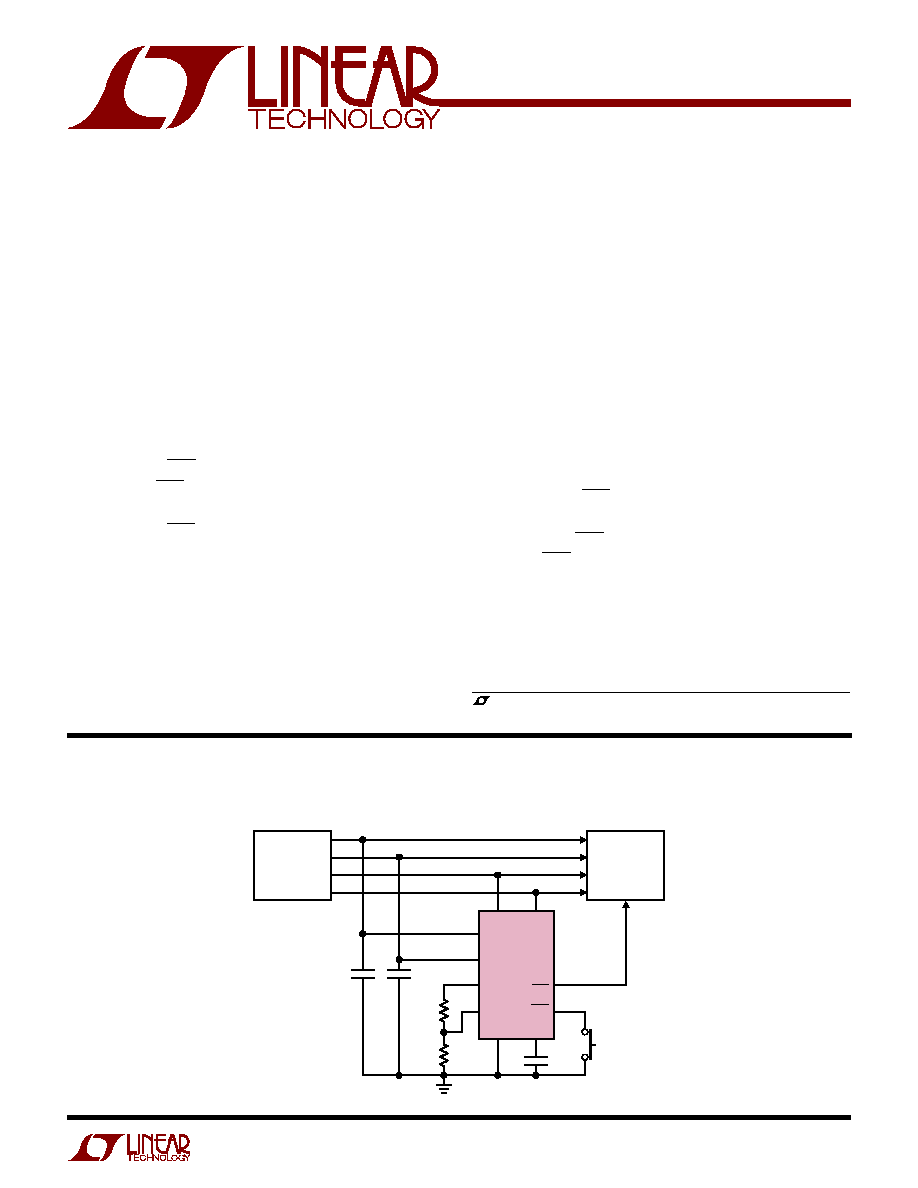
The LTC
®
2900 is a programmable supply monitor for
systems with up to four supply voltages. One of 16 preset
or adjustable voltage monitor combinations can be se-
lected using an external resistor divider connected to the
program pin. The preset voltage thresholds are accurate
to
±
1.5% over temperature.
The reset delay time is adjustable using an external
capacitor and the manual reset input may be used with a
momentary switch to issue reset pulses with programmed
duration. Tight voltage threshold accuracy and glitch
immunity ensure reliable reset operation without false
triggering. The RST output is guaranteed to be in the
correct state for V
CC
down to 1V. The LTC2900-1 features
an open-drain RST output, while the LTC2900-2 has a
push-pull RST output.
The 43
µ
A supply current makes the LTC2900 ideal for
power conscious systems and it may be configured to
monitor less than four inputs. The parts are available in
the 10-lead MSOP and the 10-lead 3mm
×
3mm DFN
packages.
s
Desktop and Notebook Computers
s
Multivoltage Systems
s
Telecom Equipment
s
Portable Battery-Powered Equipment
s
Network Servers
, LTC and LT are registered trademarks of Linear Technology Corporation.
V1
V2
V
REF
V
PG
GND
R1
59k
1%
R2
40.2k
1%
1.8V
C
RT
47nF
PUSH-BUTTON
RESET
C2
0.1
µ
F
C1
0.1
µ
F
V3
V4
LTC2900-2
CRT
PBR
RST
t
RST
= 216ms
2900 TA01
SYSTEM
LOGIC
DC/DC
CONVERTER
2.5V
3.3V
5V
Quad Supply Monitor (5V, 3.3V, 2.5V, 1.8V)
DESCRIPTIO
U
FEATURES
APPLICATIO S
U
TYPICAL APPLICATIO
U
2
LTC2900
2900f
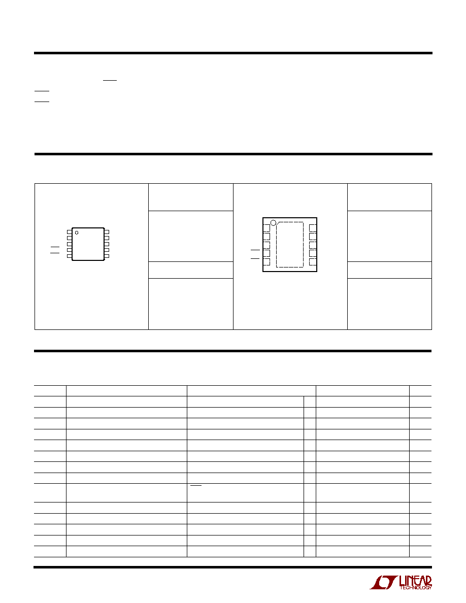
ORDER PART
NUMBER
MS PART MARKING
LTYJ
LTYL
LTYK
LTYM
T
JMAX
= 125
°
C,
JA
= 250
°
C/W
V1, V2, V3, V4, V
PG
, PBR ............................. 0.3V to 7V
RST (LTC2900-1)........................................ 0.3V to 7V
RST (LTC2900-2).......................... 0.3V to (V2 + 0.3V)
CRT ............................................. 0.3V to (V
CC
+ 0.3V)
V
REF
............................................. 0.3V to (V
CC
+ 0.3V)
Reference Load Current (I
VREF
) ............................
±
1mA
LTC2900-1CMS
LTC2900-2CMS
LTC2900-1IMS
LTC2900-2IMS
ABSOLUTE AXI U RATI GS
W
W
W
U
PACKAGE/ORDER I FOR ATIO
U
U
W
1
2
3
4
5
V3
V1
CRT
RST
PBR
10
9
8
7
6
V2
V4
V
REF
V
PG
GND
TOP VIEW
MS PACKAGE
10-LEAD PLASTIC MSOP
Consult LTC Marketing for parts specified with wider operating temperature ranges.
V4 Input Current ( ADJ Mode) ............................ 1mA
Operating Temperature Range
LTC2900-1C/LTC2900-2C ....................... 0
°
C to 70
°
C
LTC2900-1I/LTC2900-2I .................... 40
°
C to 85
°
C
Storage Temperature Range .................. 65
°
C to 150
°
C
Lead Temperature (Soldering, 10 sec)................... 300
°
C
(Notes 1, 2, 3)
ORDER PART
NUMBER
DD PART MARKING
LABU
LABW
LABV
LABX
LTC2900-1CDD
LTC2900-2CDD
LTC2900-1IDD
LTC2900-2IDD
T
JMAX
= 125
°
C,
JA
= 43
°
C/W
SYMBOL
PARAMETER
CONDITIONS
MIN
TYP
MAX
UNITS
V
RT50
5V, 5% Reset Threshold
V1 Input Threshold
q
4.600
4.675
4.750
V
V
RT33
3.3V, 5% Reset Threshold
V1, V2 Input Threshold
q
3.036
3.086
3.135
V
V
RT30
3V, 5% Reset Threshold
V2 Input Threshold
q
2.760
2.805
2.850
V
V
RT25
2.5V, 5% Reset Threshold
V2, V3 Input Threshold
q
2.300
2.338
2.375
V
V
RT18
1.8V, 5% Reset Threshold
V3, V4 Input Threshold
q
1.656
1.683
1.710
V
V
RT15
1.5V, 5% Reset Threshold
V3, V4 Input Threshold
q
1.380
1.403
1.425
V
V
RTA
ADJ Reset Threshold
V3, V4 Input Threshold
q
0.492
0.500
0.508
V
V
RTAN
ADJ Reset Threshold
V4 Input Threshold
q
18
0
18
mV
V
CC
Minimum Internal Operating Voltage
RST in Correct Logic State,
q
1
V
V
CC
Rising Prior to Program
V
CCMINP
Minimum Required for Programming
V
CC
Rising
q
2.42
V
V
REF
Reference Voltage
V
CC
2.3V, I
VREF
=
±
1mA, C
REF
1000pF
q
1.192
1.210
1.228
V
V
PG
Programming Voltage Range
V
CC
V
CCMINP
q
0
V
REF
V
I
VPG
V
PG
Input Current
V
PG
= V
REF
q
±
20
nA
I
V1
V1 Input Current
V1 = 5V, I
VREF
= 12
µ
A, (Note 4)
q
43
75
µ
A
The
q
denotes the specifications which apply over the full operating
temperature range, otherwise specifications are at T
A
= 25
°
C. V
CC
= 5V, unless otherwise noted. (Note 3)
ELECTRICAL CHARACTERISTICS
TOP VIEW
DD PACKAGE
10-LEAD (3mm
×
3mm) PLASTIC DFN
10
9
6
7
8
4
5
3
2
1
V2
V4
V
REF
V
PG
GND
V3
V1
CRT
RST
PBR
3
LTC2900
2900f
The
q
denotes the specifications which apply over the full operating
temperature range, otherwise specifications are at T
A
= 25
°
C. V
CC
= 5V, unless otherwise noted. (Note 3)
ELECTRICAL CHARACTERISTICS
Note 1: Absolute Maximum Ratings are those values beyond which the life of
a device may be impaired.
Note 2: All currents into pins are positive, all voltages are referenced to GND
unless otherwise noted.
Note 3: The greater of V1, V2 is the internal supply voltage (V
CC
).
Note 4: Under static no-fault conditions, V1 will necessarily supply quiescent
current. If at any time V2 is larger than V1, V2 must be capable of supplying
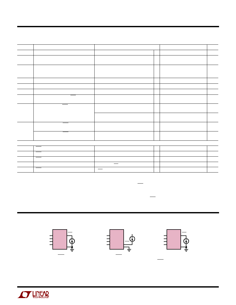
TEST CIRCUITS
V1
V2
V3
V4
2900 F01
LTC2900-1
RST
I
SOURCE
1
µ
A
V1
V2
V3
V4
2900 F02
LTC2900-1
RST
I
SINK
2.5mA,
100
µ
A
V1
V2
V3
V4
2900 F03
LTC2900-2
RST
I
SOURCE
200
µ
A
Figure 1. RST V
OH
Test
Figure 2. RST V
OL
Test
Figure 3. Active Pull-Up
RST V
OH
Test
the quiescent current, programming (transient) current and reference load
current.
Note 5: The RST output pin on the LTC2900-1 has an internal pull-up to V2
of typically 6
µ
A. However, an external pull-up resistor may be used when
faster rise times are required or for V
OH
voltages greater than V2.
Note 6: The push-pull RST output pin on the LTC2900-2 is
actively pulled up
to V2.
SYMBOL
PARAMETER
CONDITIONS
MIN
TYP
MAX
UNITS
I
V2
V2 Input Current
V2 = 3.3V
q
0.8
2
µ
A
I
V3
V3 Input Current
V3 = 2.5V
q
0.52
1.2
µ
A
V3 = 0.55V (ADJ Mode)
q
15
15
nA
I
V4
V4 Input Current
V4 = 1.8V
q
0.34
0.8
µ
A
V4 = 0.55V (ADJ Mode)
q
15
15
nA
V4 = 0.05V (ADJ Mode)
q
15
15
nA
I
CRT(UP)
CRT Pull-Up Current
V
CRT
= 0V
q
1.4
2
2.6
µ
A
I
CRT(DN)
CRT Pull-Down Current
V
CRT
= 1.3V
q
10
20
30
µ
A
t
RST
Reset Time-Out Period
C
RT
= 1500pF
q
5
7
9
ms
t
UV
V
X
Undervoltage Detect to RST
V
X
Less Than Reset Threshold V
RTX
150
µ
s
by More Than 1%
V
OL
Output Voltage Low RST
I
SINK
= 2.5mA; V1 = 3V, V2 = 3V;
q
0.15
0.4
V
V3, V4 = 0V; V
PG
= 0V
I
SINK
= 100
µ
A; V2 = 1V; V1, V3, V4 = 0V
q
0.05
0.3
V
I
SINK
= 100
µ
A; V1 = 1V; V2, V3, V4 = 0V
q
0.05
0.3
V
V
OH
Output Voltage High RST (LTC2900-1)
I
SOURCE
= 1
µ
A
q
V2 1
V
(Note 5)
Output Voltage High RST (LTC2900-2)
I
SOURCE
= 200
µ
A
q
0.8 · V2
V
(Note 6)
Manual Reset Pin
V
IH
PBR Input Threshold High
V
CC
= 3.3V to 5.5V
q
1.6
V
V
IL
PBR Input Threshold Low
V
CC
= 3.3V to 5.5V
q
0.4
V
t
PBW
PBR Input Pulse Width
V
CC
= 3.3V
q
150
ns
t
PBD
Manual Reset Propagation Delay
V
CC
= 3.3V, V
PBR
Falling
q
0.1
1
µ
s
I
PBR
PBR Pull-Up Current
V
PBR
= 0V
10
µ
A
4
LTC2900
2900f
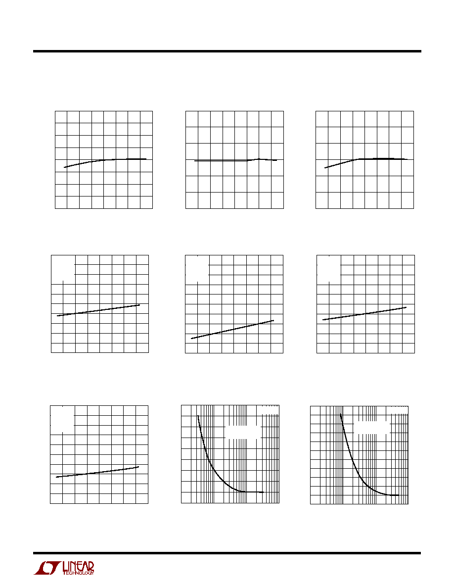
TYPICAL PERFOR A CE CHARACTERISTICS
U
W
2.5V Threshold Voltage
vs Temperature
1.8V Threshold Voltage
vs Temperature
1.5V Threshold Voltage
vs Temperature
TEMPERATURE (
°
C)
60
THRESHOLD VOLTAGE, V
RT25
(V)
2.3750
2.3675
2.3600
2.3525
2.3450
2.3375
2.3300
2.3225
2.3150
2.3075
2.3000
20
20
40
2900 G04
40
0
60
80
100
TEMPERATURE (
°
C)
60
1.655
THRESHOLD VOLTAGE, V
RT18
(V)
1.665
1.675
1.685
1.695
20
20
60
100
2900 G05
1.705
1.660
1.670
1.680
1.690
1.700
1.710
40
0
40
80
TEMPERATURE (
°
C)
60
THRESHOLD VOLTAGE, V
RT15
(V)
1.425
1.420
1.415
1.410
1.405
1.400
1.395
1.390
1.385
1.380
20
20
40
2900 G06
40
0
60
80
100
5V Threshold Voltage
vs Temperature
3.3V Threshold Voltage
vs Temperature
3V Threshold Voltage
vs Temperature
TEMPERATURE (
°
C)
60
THESHOLD VOLTAGE, V
RT50
(V)
4.675
4.700
4.750
4.725
0
40
100
2900 G01
4.650
4.625
4.600
40 20
20
60
80
TEMPERATURE (
°
C)
60
THRESHOLD VOLTAGE, V
RT33
(V)
3.135
3.125
3.115
3.105
3.095
3.085
3.075
3.065
3.055
3.045
3.035
20
20
40
2900 G02
40
0
60
80
100
TEMPERATURE (
°
C)
60
THRESHOLD VOLTAGE, V
RT30
(V)
2.850
2.840
2.830
2.820
2.810
2.800
2.790
2.780
2.770
2.760
20
20
40
2900 G03
40
0
60
80
100
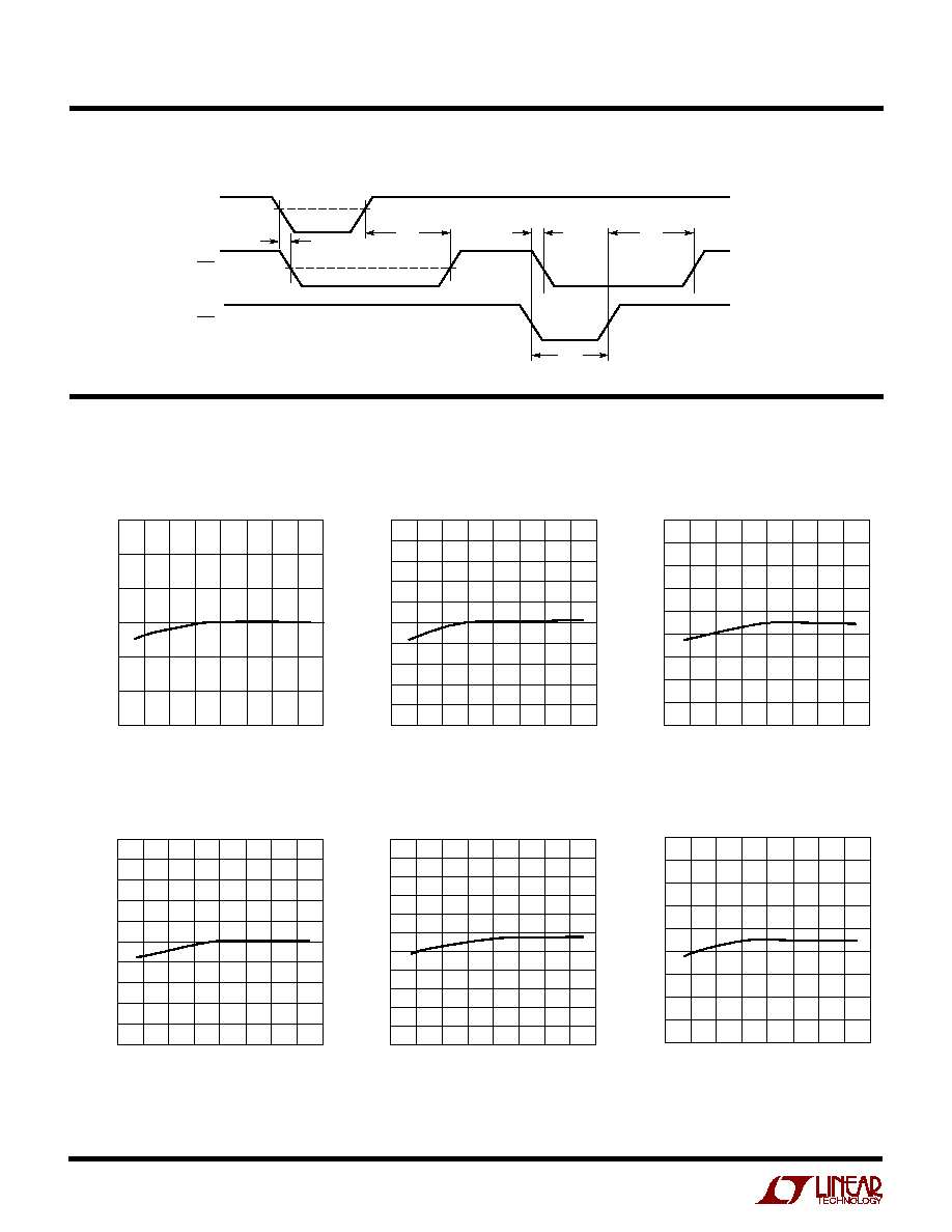
TI I G DIAGRA
U
W
W
Monitor Timing
t
RST
t
RST
t
PBW
2900 TD
V
RTX
V
X
RST
PBR
t
UV
1.5V
t
PBD
5
LTC2900
2900f
TYPICAL PERFOR A CE CHARACTERISTICS
U
W
Typical Transient Duration
vs Comparator Overdrive (V1, V2)
RESET COMPARATOR OVERDRIVE VOLTAGE (% OF V
RTX
)
0.1
250
TYPICAL TRANSIENT DURATION (
µ
s)
300
350
400
450
1
10
100
2900 G13
200
150
50
0
100
RESET OCCURS
ABOVE CURVE
T
A
= 25
°
C
RESET COMPARATOR OVERDRIVE VOLTAGE (% OF V
RTX
)
0.1
80
TYPICAL TRANSIENT DURATION (
µ
s)
100
120
140
160
1
10
100
2900 G20
60
40
20
0
200
180
220
T
A
= 25
°
C
RESET OCCURS
ABOVE CURVE
Typical Transient Duration
vs Comparator Overdrive (V3, V4)
I
V4
vs Temperature
TEMPERATURE (
°
C)
60
0
I
V4
(
µ
A)
0.1
0.3
0.4
0.5
1.0
0.7
20
20
40
2900 G12
0.2
0.8
0.9
0.6
40
0
60
80
100
V1 = 5V
V2 = 3.3V
V3 = 2.5V
V4 = 1.8V
I
V1
vs Temperature
TEMPERATURE (
°
C)
60
0
I
V1
(
µ
A)
10
30
40
50
100
70
20
20
40
2900 G09
20
80
90
60
40
0
60
80
100
V1 = 5V
V2 = 3.3V
V3 = 2.5V
V4 = 1.8V
I
V2
vs Temperature
I
V3
vs Temperature
TEMPERATURE (
°
C)
60
0.5
I
V2
(
µ
A)
0.6
0.8
0.9
1.0
1.5
1.2
20
20
40
2900 G10
0.7
1.3
1.4
1.1
40
0
60
80
100
V1 = 5V
V2 = 3.3V
V3 = 2.5V
V4 = 1.8V
TEMPERATURE (
°
C)
60
0.1
I
V3
(
µ
A)
0.2
0.4
0.5
0.6
1.1
0.8
20
20
40
2900 G11
0.3
0.9
1.0
0.7
40
0
60
80
100
V1 = 5V
V2 = 3.3V
V3 = 2.5V
V4 = 1.8V
ADJ Threshold Voltage
vs Temperature
ADJ Threshold Voltage
vs Temperature
TEMPERATURE (
°
C)
60
THRESHOLD VOLTAGE, V
RTA
(V)
0.508
0.506
0.504
0.502
0.500
0.498
0.496
0.494
0.492
20
20
40
2900 G07
40
0
60
80
100
TEMPERATURE (
°
C)
60
THRESHOLD VOLTAGE, V
RTAN
(V)
0.018
0.012
0.006
0
0.006
0.012
0.018
20
20
40
2900 G08
40
0
60
80
100
TEMPERATURE (
°
C)
60
V
REF
(V)
1.228
1.222
1.216
1.210
1.204
1.198
1.192
20
20
40
2900 G21
40
0
60
80
100
V
REF
vs Temperature