Äîêóìåíòàöèÿ è îïèñàíèÿ www.docs.chipfind.ru
LTC2904/LTC2905
1
sn29045 29045fs
FEATURES
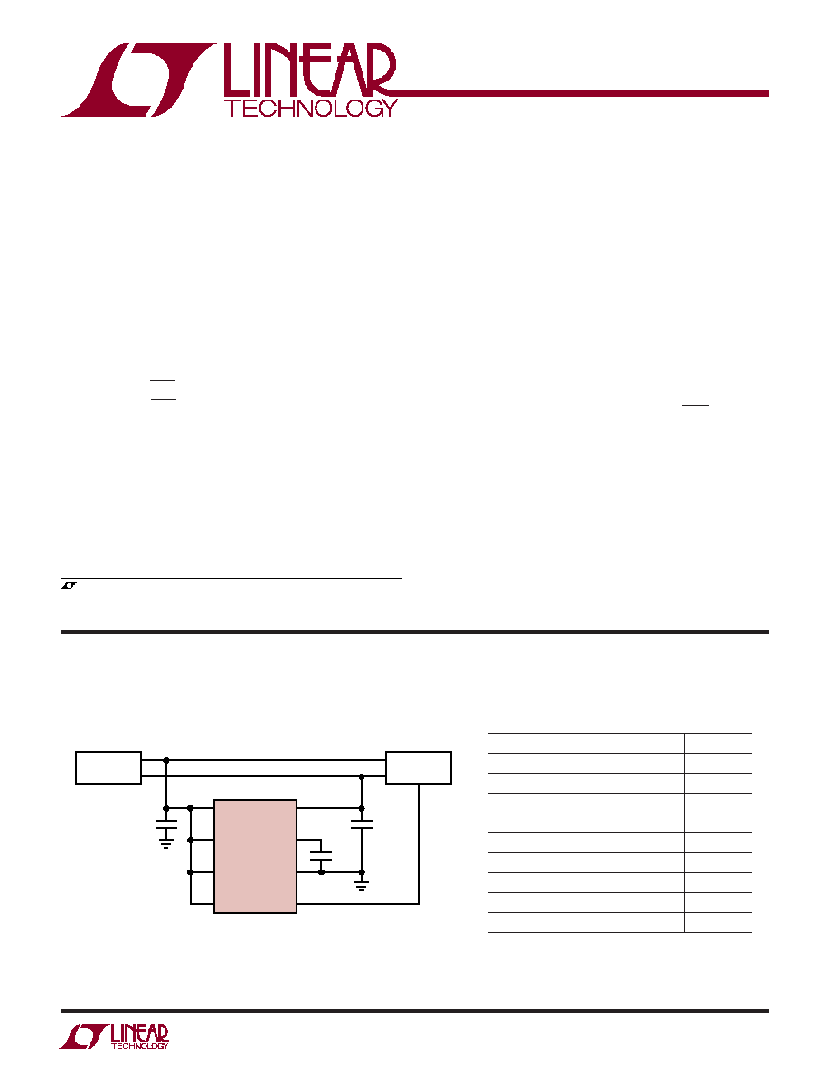
TYPICAL APPLICATIO
U
DESCRIPTIO
U
Monitors Two Inputs Simultaneously
Nine Threshold Combinations
Three Supply Tolerances (5%, 7.5%, 10%)
Guaranteed Threshold Accuracy: ±1.5% of
Monitored Voltage Over Temperature
Internal V
CC
Auto Select
Power Supply Glitch Immunity
200ms Reset Time Delay (LTC2904 Only)
Adjustable Reset Time Delay (LTC2905 Only)
Open Drain RST Output
Guaranteed RST for V1 1V or V2 1V
Low Profile (1mm) SOT-23 (ThinSOT
TM
) and Plastic
(3mm x 2mm) DFN Packages
Desktop and Notebook Computers
Handheld Devices
Network Servers
Core, I/O Monitor
Precision Dual Supply Monitors
with Pin-Selectable Thresholds
The LTC
®
2904/LTC2905 are dual supply monitors in-
tended for systems with two supply voltages. The dual
supply monitors have a common reset output with delay
(200ms for the LTC2904 and adjustable using an external
capacitor for the LTC2905). This product provides a
precise, space-conscious and micropower solution for
supply monitoring.
The LTC2904/LTC2905 feature a tight 1.5% threshold
accuracy over the whole operating temperature range,
and glitch immunity to ensure reliable reset operation
without false triggering. The open drain RST output is
guaranteed to be in the correct state for inputs down to 1V.
The LTC2904/LTC2905 also feature three programming
input pins, which program the threshold and tolerance
level without requiring any external components. These
three programming pins provide a total of 27 different
voltage level and tolerance combinations, eliminating
the need to have different parts for development and
implementation of different systems with different voltage
levels requiring monitoring function.
, LTC and LT are registered trademarks of Linear Technology Corporation.
V1
S1
S2
TOL
V2
TMR
GND
RST
LTC2905
22nF
0.1µF
0.1µF
DC/DC
CONVERTER
SYSTEM
LOGIC
29045 TA01
3.3V
5V
5V, 3.3V Dual Supply Monitor with 5% Tolerance
Table 1. Voltage Threshold Programming
V1
V2
S1
S2
5.0
3.3
V1
V1
3.3
2.5
Open
GND
3.3
1.8
V1
Open
3.3
1.5
Open
V1
3.3
1.2
Open
Open
2.5
1.8
GND
GND
2.5
1.5
GND
Open
2.5
1.2
GND
V1
2.5
1.0
V1
GND
APPLICATIO S
U
ThinSOT is a trademark of Linear Technology Corporation.
LTC2904/LTC2905
2
sn29045 29045fs
Terminal Voltages
V1, V2 ..................................................... 0.3V to 7V
S1, S2, TOL .............................. 0.3V to (V
CC
+0.3V)
RST ......................................................... 0.3V to 7V
RST (LTC2904) ....................................... 0.3V to 7V
TMR (LTC2905) ...................................... 0.3V to 7V
ORDER PART
NUMBER
DDB8 PART MARKING
T
JMAX
= 125°C,
JA
= 250°C/W
LBCZ
LBDB
LTAJF
LBCY
ABSOLUTE AXI U
RATI GS
W
W
W
U
PACKAGE/ORDER I FOR ATIO
U
U
W
(Note 1, 2)
ELECTRICAL CHARACTERISTICS
The
denotes the specifications which apply over the full operating
temperature range, otherwise specifications are at T
A
= 25°C. V1 = 2.5V, V2 = 1V, S1 = TOL = V1, S2 = 0V, unless otherwise noted.
(Notes 2, 3, 4)
SYMBOL
PARAMETER
CONDITIONS
MIN
TYP
MAX
UNITS
V
RT50
5V, 5% Reset Threshold
V1 Input Threshold
4.600
4.675
4.750
V
5V, 7.5% Reset Threshold
4.475
4.550
4.625
V
5V, 10% Reset Threshold
4.350
4.425
4.500
V
V
RT33
3.3V, 5% Reset Threshold
V1, V2 Input Threshold
3.036
3.086
3.135
V
3.3V, 7.5% Reset Threshold
2.954
3.003
3.053
V
3.3V, 10% Reset Threshold
2.871
2.921
2.970
V
V
RT25
2.5V, 5% Reset Threshold
V1, V2 Input Threshold
2.300
2.338
2.375
V
2.5V, 7.5% Reset Threshold
2.238
2.275
2.313
V
2.5V, 10% Reset Threshold
2.175
2.213
2.250
V
V
RT18
1.8V, 5% Reset Threshold
V2 Input Threshold
1.656
1.683
1.710
V
1.8V, 7.5% Reset Threshold
1.611
1.638
1.665
V
1.8V, 10% Reset Threshold
1.566
1.593
1.620
V
V
RT15
1.5V, 5% Reset Threshold
V2 Input Threshold
1.380
1.403
1.425
V
1.5V, 7.5% Reset Threshold
1.343
1.365
1.388
V
1.5V, 10% Reset Threshold
1.305
1.328
1.350
V
V
RT12
1.2V, 5% Reset Threshold
V2 Input Threshold
1.104
1.122
1.140
V
1.2V, 7.5% Reset Threshold
1.074
1.092
1.110
V
1.2V, 10% Reset Threshold
1.044
1.062
1.080
V
V
RT10
1V, 5% Reset Threshold
V2 Input Threshold
0.920
0.935
0.950
V
1V, 7.5% Reset Threshold
0.895
0.910
0.925
V
1V, 10% Reset Threshold
0.870
0.885
0.900
V
Consult LTC Marketing for parts specified with wider operating temperature ranges.
Operating Temperature Range
LTC2904C/LTC2905C ................................ 0°C to 70°C
LTC2904I/LTC2905I ..............................40°C to 85°C
Storage Temperature Range ..................65°C to 150°C
Lead Temperature (Soldering, 10 sec).................. 300°C
ORDER PART
NUMBER
TS8 PART MARKING
LTC2904CDDB
LTC2904IDDB
LTC2905CDDB
LTC2905IDDB
LTC2904CTS8
LTC2904ITS8
LTC2905CTS8
LTC2905ITS8
LTBCJ
LTBCK
LTAJD
LTAJE
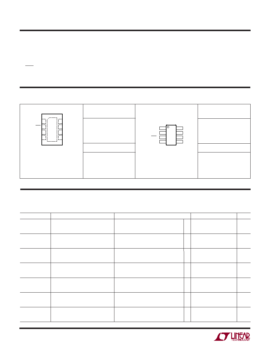
TOP VIEW
DDB8 PACKAGE
8-LEAD (3mm × 2mm) PLASTIC DFN
EXPOSED PAD IS GND (PIN 9),
MUST BE SOLDERED TO PCB
5
6
7
8
4
3
2
1
GND
RST
RST/TMR*
V2
TOL
S1
S2
V1
9
V2 1
RST/TMR* 2
RST 3
GND 4
8 V1
7 S2
6 S1
5 TOL
TOP VIEW
TS8 PACKAGE
8-LEAD PLASTIC TSOT-23
T
JMAX
= 125°C,
JA
= 250°C/W
* RST FOR LTC2904
TMR FOR LTC2905
* RST FOR LTC2904
TMR FOR LTC2905
LTC2904/LTC2905
3
sn29045 29045fs
ELECTRICAL CHARACTERISTICS
The
denotes the specifications which apply over the full operating
temperature range, otherwise specifications are at T
A
= 25°C. V1 = 2.5V, V2 = 1V, S1 = TOL = V1, S2 = 0V, unless otherwise noted.
(Notes 2, 3)
Note 1: Absolute Maximum Ratings are those values beyond which the life
of a device may be impaired.
Note 2: The greater of V1, V2 is the internal supply voltage (V
CC
).
Note 3: All currents into pins are positive; all voltages are referenced to
GND unless otherwise noted.
Note 4: For reset thresholds test conditions refer to the voltage threshold
programming table in the Applications Information section.
Note 5: The output pins RST and RST have an internal pull-up to V
CC
of
typically 6µA. However, an external pull-up resistor may be used when
faster rise time is required or for V
OH
voltages greater than V
CC
.
Note 6: The input current to the three-state input pins are the pull-up and
the pull-down current when the pins are either set to V1 or GND
respectively. In the open state, the maximum leakage current to V1 or GND
permissible is 10µA.
SYMBOL
PARAMETER
CONDITIONS
MIN
TYP
MAX
UNITS
V
CCMIN
Minimum Internal Operating Voltage (Note 2) RST in Correct Logic State
1
V
I
V1
V1 Input Current
Includes Input Current to Three-State Pins
65
130
µA
I
V2
V2 Input Current
0.4
1.0
µA
I
TMR(UP)
TMR Pull-Up Current
(LTC2905)
V
TMR
= 0V
1.5
2.1
2.7
µA
I
TMR(DOWN)
TMR Pull-Down Current
(LTC2905)
V
TMR
= 1.4V
1.5
2.1
2.7
µA
t
RST
Reset Time-Out Period
(LTC2904)
140
200
260
ms
t
RST
Reset Time-Out Period
(LTC2905)
C
TMR
= 22nF
140
200
260
ms
t
UV
Vx Undervoltage Detect to
Vx Less than Reset Threshold V
RTX
150
µs
RST or RST
by More than 1%
V
OL
Output Voltage Low RST, RST
I = 2.5mA
0.15
0.4
V
I = 100µA; V1 = 1V (RST Only)
0.05
0.3
V
V
OH
Output Voltage High RST, RST
I = 1µA
V
CC
1
V
(Notes 2, 5)
Three-State Inputs S1, S2, TOL
V
IL
Low Level Input Voltage
0.4
V
V
IH
High Level Input Voltage
1.4
V
V
Z
Pin Voltage when Left in Open State
I = 10µA
0.7
V
I = 0µA
0.9
V
I = 10µA
1.1
V
I
VPG
Programming Input Current (Note 6)
±25
µA

LTC2904/LTC2905
4
sn29045 29045fs
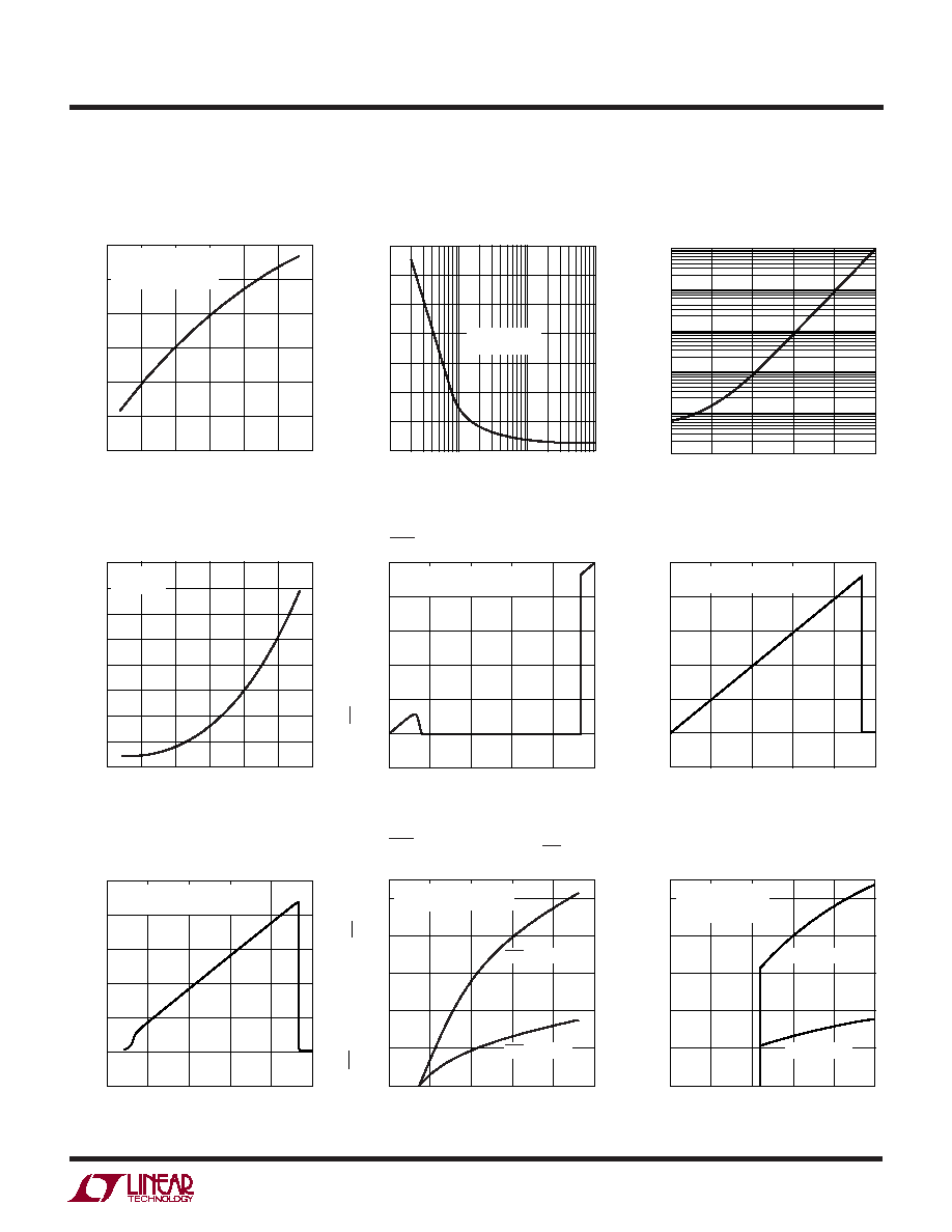
TEMPERATURE (°C)
THRESHOLD VOLTAGE, V
RT50
(V)
29045 G01
TEMPERATURE (°C)
TEMPERATURE (°C)
TEMPERATURE (°C)
TEMPERATURE (°C)
TEMPERATURE (°C)
TEMPERATURE (°C)
TEMPERATURE (°C)
TEMPERATURE (°C)
THRESHOLD VOLTAGE, V
RT33
(V)
3.120
3.070
3.020
2.970
2.920
2.870
29045 G02
THRESHOLD VOLTAGE, V
RT25
(V)
29045 G03
2.375
2.325
2.275
2.225
2.175
THRESHOLD VOLTAGE, V
RT18
(V)
29045 G04
1.705
1.685
1.665
1.645
1.625
1.605
1.585
1.565
THRESHOLD VOLTAGE, V
RT15
(V)
29045 G05
1.425
1.405
1.385
1.365
1.345
1.325
1.305
THRESHOLD VOLTAGE, V
RT12
(V)
1.135
1.125
1.115
1.105
1.095
1.085
1.075
1.065
1.055
1.045
29045 G06
THRESHOLD VOLTAGE, V
RT10
(V)
29045 G07
0.950
0.940
0.930
0.920
0.910
0.900
0.890
0.880
0.870
4.75
4.70
4.65
4.60
4.55
4.50
4.45
4.40
4.35
I
V1
(
µ
A)
21.5
21.0
20.5
20.0
19.5
19.0
29045 G08
I
V2
(
µ
A)
29045 G09
1.8
1.7
1.6
1.5
1.4
1.3
1.2
50
100
25
75
25
0
50
50
100
25
75
25
0
50
50
100
25
75
25
0
50
50
100
25
75
25
0
50
50
100
25
75
25
0
50
50
100
25
75
25
0
50
50
100
25
75
25
0
50
50
100
25
75
25
0
50
50
100
25
75
25
0
50
5%
7.5%
10%
5%
7.5%
10%
5%
7.5%
10%
5%
7.5%
10%
5%
7.5%
10%
5%
7.5%
10%
5%
7.5%
10%
V1 = 5V
V2 = 3.3V
S1 = S2 = TOL = 1.4V
V1 = 5V
V2 = 3.3V
S1 = S2 = TOL = 1.4V
5V Threshold Voltage vs
Temperature
3.3V Threshold Voltage vs
Temperature
2.5V Threshold Voltage vs
Temperature
1.8V Threshold Voltage vs
Temperature
1.5V Threshold Voltage vs
Temperature
1.2V Threshold Voltage vs
Temperature
1V Threshold Voltage vs
Temperature
I
V1
vs Temperature
I
V2
vs Temperature
TYPICAL PERFOR A CE CHARACTERISTICS
U
W
Specifications are at T
A
= 25°C unless otherwise noted.
LTC2904/LTC2905
5
sn29045 29045fs
TEMPERATURE (°C)
I
V2
(
µ
A)
29045 G10
20.0
19.5
19.0
18.5
18.0
17.5
17.0
COMPARATOR OVERDRIVE VOLTAGE (% OF V
RTX
)
0.1
TYPICAL TRANSIENT DURATION (
µ
s)
700
600
500
400
300
200
100
0
1
10
100
29045 G11
RESET OCCURS
ABOVE CURVE
C
TMR
(FARAD)
10p
100p
1n
10n
100n
1µ
RESET TIME OUT PERIOD, t
RST
(ms)
29045 G12
10000
1000
100
10
1
0.1
TEMPERATURE (°C)
RESET TIME-OUT PERIOD, t
RST
(ms)
29045 G13
235
230
225
220
215
210
205
200
195
V1 (V)
0
RST OUTPUT VOLTAGE (V)
5
4
3
2
1
0
1
1
2
3
4
29045 G14
5
V2 = S1 = S2 = TOL = V1
10k PULL-UP RESISTOR
V1 (V)
0
RST OUTPUT VOLTAGE (V)
5
4
3
2
1
0
1
1
2
3
4
29045 G15
5
V2 = S1 = S2 = TOL = V1
10k PULL-UP RESISTOR
SUPPLY VOLTAGE, V
CC
(V)
0
RST PULL-DOWN CURRENT, I
RST
(mA)
5
4
3
2
1
0
4
29045 G17
1
2
3
5
RST AT 150mV
RST AT 50mV
V1 (V)
0
RST OUTPUT VOLTAGE (V)
5
4
3
2
1
0
1
1
2
3
4
29045 G16
5
V2 = S1 = S2 = TOL = V1
10pF CAPACITOR AT RST
SUPPLY VOLTAGE, V
CC
(V)
0
RST PULL-DOWN CURRENT, I
RST
(mA)
5
4
3
2
1
0
4
29045 G18
1
2
3
5
RST AT 150mV
RST AT 50mV
S1 = V2 = V1
TOL = S2 = GND
NO PULL-UP R
V2 = S1 = S2 = TOL = V1
NO PULL-UP R
50
100
25
75
25
0
50
50
100
25
75
25
0
50
CRT = 22nF
(FILM)
V1 = 2.5V
V2 = 3.3V
S1 = S2 = TOL = 1.4V
TYPICAL PERFOR A CE CHARACTERISTICS
U
W
I
V2
vs Temperature
Typical Transient Duration vs
Comparator Overdrive (V1, V2)
Reset Time Out Period (t
RST
)
vs Capacitance (C
TMR
)
Reset Time-Out Period (t
RST
)
vs Temperature
RST Output Voltage vs V1
RST Output Voltage vs V1
RST Output Voltage vs V1
RST Pull-Down Current (I
RST
)
vs Supply Voltage (V
CC
)
RST Pull-Down Current (I
RST
)
vs Supply Voltage (V
CC
)
Specifications are at T
A
= 25°C unless otherwise noted.