 | –≠–ª–µ–∫—Ç—Ä–æ–Ω–Ω—ã–π –∫–æ–º–ø–æ–Ω–µ–Ω—Ç: LTC2951 | –°–∫–∞—á–∞—Ç—å:  PDF PDF  ZIP ZIP |

LTC2951
1
2951f
EN
2V/DIV
PB
25ms/DIV
2951 TA01b
128ms
Push Button On/Off
Controller
The LTC
Æ
2951 is a micropower, wide input voltage range
push button ON/OFF controller. The part contains a push
button input which controls the toggling of an open drain
enable output. The push button turn OFF debounce time
is externally programmable, while the turn ON debounce
time is fi xed at 128ms. A simple microprocessor interface
allows for proper system housekeeping prior to power
down. Under system fault conditions, an adjustable KILL
timeout delay ensures proper power down.
The LTC2951 operates over a 2.7V to 26V input voltage
range to accommodate a variety of input power supplies.
Very low quiescent current (6µA typical) makes the
LTC2951 ideally suited for battery powered applications.
Two versions of the part are available to accommodate
either positive or negative enable polarities. The parts
are available in 8-pin 3mm ◊ 2mm DFN and ThinSOT
packages.
Portable Instrumentation Meters
Blade Servers
Portable Customer Service PDA
Desktop and Notebook Computers
Adjustable Push Button Debounce and Delay
Timers
Low Supply Current: 6µA
Wide Operating Voltage Range: 2.7V to 26V
EN Output (LTC2951-1) Allows DC/DC Converter
Control
EN Output (LTC2951-2) Allows Circuit Breaker
Control
Simple Interface Allows Graceful µP Shut Down
High Input Voltage PB Pin with Internal Pull Up
Resistor
±10kV ESD HBM on PB Input
Accurate 0.6V Threshold on KILL Comparator Input
8-Pin 3mm ◊ 2mm DFN and ThinSOT
TM
Packages
V
IN
SHDN
V
IN
V
OUT
EN
INT
KILL
INT
KILL
LTC2951-1
KILLT
OFFT
DC/DC
BUCK
µP/µC
3V ≠ 26V
*OPTIONAL
R1
10k
2951 TA01
C
KILLT
*
0.033
µF
C
OFFT
*
0.033
µF
PB
GND
V
IN
, LTC and LT are registered trademarks of Linear Technology Corporation. ThinSOT is
a trademark of Linear Technology Corporation. All other trademarks are the property of
their respective owners.
APPLICATIO S
U
FEATURES
DESCRIPTIO
U
TYPICAL APPLICATIO
U
Turn On Debounce

LTC2951
2
2951f
Supply Voltage (V
IN
) ..................................≠ 0.3V to 33V
Input Voltages
PB ............................................................≠ 6V to 33V
KILLT ....................................................≠ 0.3V to 2.7V
OFFT .....................................................≠ 0.3V to 2.7V
KILL .........................................................≠ 0.3V to 7V
Output Voltages
INT .........................................................≠ 0.3V to 10V
EN/EN ....................................................≠ 0.3V to 10V
(Note 1)
Operating Temperature Range
LTC2951C-1 .............................................. 0∞C to 70∞C
LTC2951C-2 .............................................. 0∞C to 70∞C
LTC2951I-1 .......................................... ≠ 40∞C to 85∞C
LTC2951I-2 .......................................... ≠ 40∞C to 85∞C
Storage Temperature Range
DFN Package ..................................... ≠ 65∞C to 125∞C
TSOT-23 ............................................ ≠ 65∞C to 150∞C
Lead Temperature (Soldering, 10 sec) .................. 300∞C
ORDER PART
NUMBER
DDB PART*
MARKING
T
JMAX
= 125∞C,
JA
= 165∞C/W
EXPOSED PAD (PIN 9) UNCONNECTED
Consult LTC Marketing for parts specifi ed with wider operating temperature ranges. *The temperature grade is identifi ed by a label on the shipping container.
LBTB
LBTD
LBTB
LBTD
T
JMAX
= 125∞C,
JA
= 140∞C/W
ORDER PART
NUMBER
TS8 PART*
MARKING
LTBTC
LTBTF
LTBTC
LTBTF
LTC2951CDDB-1
LTC2951CDDB-2
LTC2951IDDB-1
LTC2951IDDB-2
LTC2951CTS8-1
LTC2951CTS8-2
LTC2951ITS8-1
LTC2951ITS8-2
V
IN
1
PB 2
KILLT 3
GND 4
8 KILL
7 OFFT
6 EN/EN
5 INT
TOP VIEW
TS8 PACKAGE
8-LEAD PLASTIC TSOT-23
TOP VIEW
DDB8 PACKAGE
8-LEAD (3mm
◊ 2mm) PLASTIC DFN
5
6
7
8
9
4
3
2
1
INT
EN/EN
OFFT
KILL
GND
KILLT
PB
V
IN
The
denotes the specifi cations which apply over the full operating
temperature range, otherwise specifi cations are at T
A
= 25∞C. V
IN
= 2.7V to 26.4V, unless otherwise noted. (Note 2)
SYMBOL PARAMETER
CONDITIONS
MIN
TYP
MAX
UNITS
V
IN
Supply Voltage Range
Steady State Operation
2.7
26.4
V
I
IN
V
IN
Supply Current
System Power On
6
12
µA
V
UVL
V
IN
Undervoltage Lockout
V
IN
Falling
2.2 2.3 2.4
V
V
UVL(HYST)
V
IN
Undervoltage Lockout Hysteresis
50
300 600
mV
ABSOLUTE AXI U
RATI GS
W
W
W
U
PACKAGE/ORDER I FOR ATIO
U
U
W
ELECTRICAL CHARACTERISTICS

LTC2951
3
2951f
The
denotes the specifi cations which apply over the full operating
temperature range, otherwise specifi cations are at T
A
= 25∞C. V
IN
= 2.7V to 26.4V, unless otherwise noted. (Note 2)
SYMBOL
PARAMETER
CONDITIONS
MIN
TYP
MAX
UNITS
Push Button Pin (PB)
V
PB(MIN, MAX)
PB Voltage Range
Single-Ended
≠1
26.4
V
I
PB
PB Input Current
2.5V < V
PB
< 26.4V
V
PB
= 1V
V
PB
= 0.6V
≠1
≠ 3
≠6
≠ 9
±1
≠12
≠ 15
µA
µA
µA
V
PB(VTH)
PB Input Threshold
PB Falling
0.6
0.8
1
V
V
PB(VOC)
PB Open Circuit Voltage
I
PB
= ≠ 1µA
1
1.6
2
V
Timing Pins (KILLT, OFFT)
I
KILLT, OFFT(PU)
KILLT/OFFT Pull Up Current
V
KILLT, OFFT
= 0V
≠2.4
≠3
≠3.6
µA
I
KILLT, OFFT(PD)
KILLT/OFFT Pull Down Current
V
KILLT, OFFT
= 1.3V
2.4
3
3.6
µA
t
DB, ON
Turn On Debounce Time
PB Falling Enable Asserted
100
128
163
ms
t
DB, OFF
Internal Turn Off Debounce Time
OFFT Pin Float, PB Falling INT Falling
26
32
41
ms
t
OFFT
Additional Adjustable Turn Off Time C
OFFT
= 1500pF
9
11.5
13.5
ms
µP Handshake Pins (INT, KILL)
I
INT(LKG)
INT Leakage Current
V
INT
= 3V
±1
µA
V
INT(VOL)
INT Output Voltage Low
I
INT
= 3mA
0.11
0.4
V
V
KILL(TH)
KILL Input Threshold Voltage
KILL Falling
0.57
0.6
0.63
V
V
KILL(HYST)
KILL Input Threshold Hysteresis
10
30
50
mV
I
KILL(LKG)
KILL Leakage Current
V
KILL
= 0.6V
±0.1
µA
t
KILL(PW)
KILL Minimum Pulse Width
30
µs
t
KILL(PD)
KILL Propagation Delay
KILL Falling Enable Released
30
µs
t
KILL, ON BLANK
KILL Turn On Blanking (Note 3)
KILL = Low, Enable Asserted Enable
Released
400
512
650
ms
t
KILL, OFF DELAY
Internal KILL Turn Off Delay
(Note 4)
KILLT Pin Float, KILL = High, INT Asserted
Enable Released
100
128
163
ms
t
KILL, OFF DELAY,
ADDITIONAL
Additional Adjustable KILL Turn Off
Delay (Note 4)
C
KILLT
= 1500pF
9
11.5
13.5
ms
t
EN/EN, Lock Out
EN/EN Lock Out Time (Note 5)
Enable Released Enable Asserted
200
256
325
ms
I
EN/EN(LKG)
EN/EN Leakage Current
V
EN/
EN
= 1V, Sink Current Off
±0.1
µA
V
EN/EN(VOL)
EN/EN Voltage Output Low
I
EN/
EN
= 3mA
0.11
0.4
V
Note 1: Absolute Maximum Ratings are those values beyond which the life
of a device may be impaired.
Note 2: All currents into pins are positive; all voltages are referenced to
GND unless otherwise noted.
Note 3: The KILL turn on blanking timer period is the waiting period
immediately after the enable output is asserted. This blanking time allows
suffi cient time for the DC/DC converter and the µP to perform power up
tasks. The KILL and PB inputs are ignored during this period. If KILL
remains low at the end of this time period, the enable output is released,
thus turning off system power. This time delay does not include t
DB, ON
.
Note 4: The internal KILL turn off delay (t
KILL
,
OFF DELAY
) is the default
delay from the initiation of a power off sequence (INT falling, KILL = high),
to the release of the enable output. The additional, adjustable KILL turn
off delay (t
KILL
,
OFF DELAY, ADDITIONAL
) uses an optional external capacitor
(C
KILLT
) to provide extra delay from INT falling to the release of the enable
output. If the KILL input switches low at any time during KILL turn off
delay, enable is released, thus turning off system power.
Note 5: The enable lock out time is designed to allow an application to
properly power down such that the next power up sequence starts from a
consistent powered down confi guration. PB is ignored during this lock out
time. This time delay does not include t
DB, ON
.
ELECTRICAL CHARACTERISTICS

LTC2951
4
2951f
TYPICAL PERFOR A CE CHARACTERISTICS
U
W
TEMPERATURE (
∞C)
≠50
I
VIN
(
µ
A)
10
8
6
4
2
0
≠25
0
25
50
2951 G01
75
100
0
5
10
15
20
25
30
TEMPERATURE (
∞C)
≠50
≠25
0
25
50
75
100
V
IN
(V)
I
VIN
(
µ
A)
10
8
6
4
2
0
2951 G02
2951 G03
KILLT PULL-DOWN CURRENT (
µ
A)
1
t
KILL, OFF DELAY
+ t
KILL, OFF DELAY, ADDITIONAL
(ms)
100
1000
1000
2951 G04
10
10
100
10000
2951 G05
V
IN
(V)
0
t
DB, OFF
(ms)
5
10
15
20
2951 G06
25
30
2951 G07
2951 G08
V
IN
= 26.4V
V
IN
= 3.3V
V
IN
= 2.7V
T
A
= 25
∞C
V
IN
(V)
0
0
t
KILL, OFF DELAY
(ms)
40
80
120
160
200
5
10
15
20
25
30
T
A
= 25
∞C
KILLT EXTERNAL CAPACITOR (nF)
1
t
DB, OFF
+ t
OFFT
(ms)
100
1000
1000
10
10
100
10000
T
A
= 25
∞C
V
IN
= 3.3V
OFFT EXTERNAL CAPACITOR (nF)
≠3.4
≠3.2
≠3.0
≠2.8
≠2.6
V
IN
= 26.4V
V
IN
= 2.7V
TEMPERATURE (
∞C)
≠50
≠25
0
25
50
75
100
OFFT PULL-DOWN CURRENT (
µ
A)
≠3.4
≠3.2
≠3.0
≠2.8
≠2.6
V
IN
= 26.4V
V
IN
= 2.7V
50
40
30
20
10
0
T
A
= 25
∞C
2951 G14
V
IN
(V)
0
0
t
DB, ON
(ms)
40
80
120
160
200
5
10
15
20
25
30
T
A
= 25
∞C
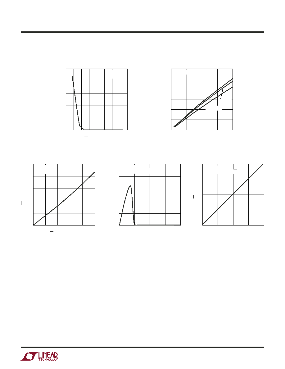
Supply Current vs Temperature
KILL Turn Off Delay vs KILLT
External Capacitor
Supply Current vs Supply Voltage
KILLT Pull-Down Current vs
Temperature
Internal Default Turn Off
Debounce Time (t
DB, OFF
) vs V
IN
Turn Off Debounce Time (t
DB, OFF
+ t
OFFT
) vs OFFT External Capacitor
OFFT Pull-Down Current vs
Temperature
Internal Default KILL Turn Off
Delay (t
KILL, OFF DELAY
) vs V
IN
Turn On Debounce Time
(t
DB, ON
) vs V
IN
LTC2951
5
2951f
EN (V)
PB CURRENT (
µ
A)
2951 G09
2951 G10
EN/EN CURRENT LOAD (mA)
0
EN/EN VOLTAGE (mV)
500
400
300
200
100
0
8
2951 G11
2
4
6
10
2951 G13
V
IN
(V)
≠10
0
10
20
30
≠5
5
15
25
≠250
≠200
≠150
≠100
≠50
0
PB VOLTAGE (V)
T
A
= 25
∞C
V
IN
= 3.3V
0
0
50
100
150
200
250
300
5
10
15
20
V
IN
= 3.3V
T
A
= 25
∞C
PB VOLTAGE (mV)
EXTERNAL PB RESISTANCE TO GROUND (k
)
T
A
= ≠45
∞C
T
A
= 100
∞C
T
A
= 25
∞C
V
IN
= 3.3V
0
4
1
2
3
4
3
2
1
0
T
A
= 25
∞C
100k PULL-UP FROM EN TO V
IN
V
IN
(V)
0
EN (V)
4
2951 G12
1
2
3
T
A
= 25
∞C
100k PULL-UP FROM EN TO V
IN
1.0
0.8
0.6
0.4
0.2
0
TYPICAL PERFOR A CE CHARACTERISTICS
U
W
PB Current vs PB Voltage
PB Voltage vs External PB
Resistance to Ground
EN/EN V
OL
vs Current Load
EN (LTC2951-2) Voltage vs V
IN
EN (LTC2951-1) Voltage vs V
IN