 | ÐлекÑÑоннÑй компоненÑ: LTC3201 | СкаÑаÑÑ:  PDF PDF  ZIP ZIP |
3201f.pm6
LTC3201
1
3201f
APPLICATIO S
U
TYPICAL APPLICATIO
U
FEATURES
DESCRIPTIO
U
The LTC
®
3201 is an ultralow noise, constant frequency,
charge pump DC/DC converter specifically designed for
powering white LEDs. The part produces a low noise
boosted supply capable of supplying 100mA of output
current. LED current is regulated for accurate and stable
backlighting. A 3-bit DAC provides output current adjust
for brightness control.
Low external parts count (one small flying capacitor and
three small bypass capacitors) and small MSOP-10 pack-
age size make the LTC3201 ideally suited for space con-
strained applications. An input noise filter further reduces
input noise, thus enabling direct connection to the battery.
High switching frequency enables the use of small external
capacitors.
The LTC3201 contains overtemperature protection and
can survive an indefinite output short to GND. Internal
soft-start circuitry also prevents excessive inrush current
on start-up. A low current shutdown feature disconnects
the load from V
IN
and reduces quiescent current to less
than 1
µ
A.
s
White LED Backlighting
s
Programmable Boost Current Source
s
Input Noise Filter Minimizes Supply Noise
s
Constant Frequency Operation
s
3-Bit LED Current Control
s
No Inductors
s
Low Shutdown Current: I
IN
< 1
µ
A
s
Output Current: 100mA
s
V
IN
Range: 2.7V to 4.5V
s
1.8MHz Switching Frequency
s
Soft-Start Limits Inrush Current at Turn-On
s
Short-Circuit and Overtemperature Protected
s
Available in 10-Pin MSOP Package
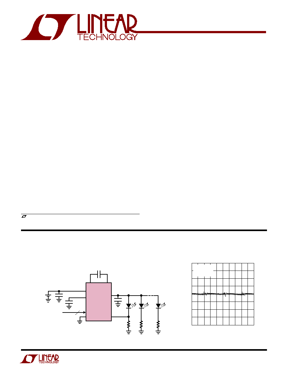
100mA Ultralow Noise
Charge Pump LED Supply
with Output Current Adjust
Ultralow Noise White LED Driver
with Adjustable Current Control
Input Current Ripple
, LTC and LT are registered trademarks of Linear Technology Corporation.
LTC3201
V
IN
CM
CP
V
OUT
D0-D2
FILTER
GND
FB
1
µ
F
1
µ
F
0.22
µ
F
0.22
µ
F
56
56
56
UP TO
6-WHITE LEDs
Li ION
LED
CURRENT
ADJUST
3
3201 TA01a
+
· · ·
3201 TA01b
50mA/DIV
I
OUT
= 100mA
I
IN
= 205mA
V
IN
= 3.6V
100ns/DIV
LTC3201
2
3201f
ABSOLUTE AXI U
RATI GS
W
W
W
U
PACKAGE/ORDER I FOR ATIO
U
U
W
(Note 1)
ELECTRICAL CHARACTERISTICS
The
q
denotes the specifications which apply over the full operating
temperature range, otherwise specifications are at T
A
= 25
°
C. V
IN
= 3.6V, C
FILTER
= C
FLY
= 0.22
µ
F, C
IN
= C
OUT
= 1
µ
F,
t
MIN
to t
MAX
unless otherwise noted.
V
IN
, V
FILTER
, V
OUT
, CP, CM to GND .............. 0.3V to 6V
D0, D1, D2, FB to GND ................. 0.3V to (V
IN
+ 0.3V)
V
OUT
Short-Circuit Duration ............................. Indefinite
I
OUT ......................................................................................
150mA
Operating Temperature Range (Note 2) ...40
°
C to 85
°
C
Storage Temperature Range ................. 65
°
C to 150
°
C
Lead Temperature (Soldering, 10 sec).................. 300
°
C
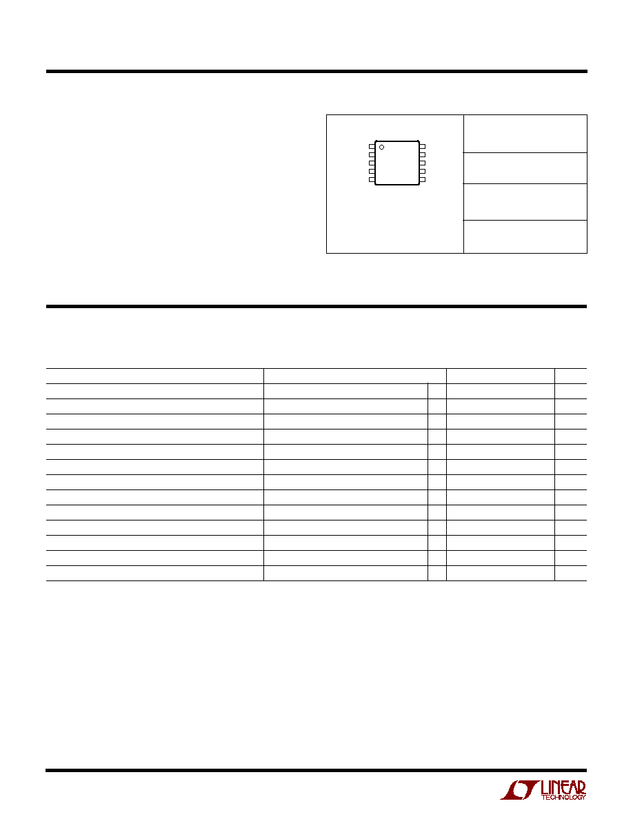
ORDER PART
NUMBER
MS PART
MARKING
T
JMAX
= 150
°
C
JA
= 130
°
C/W (1 LAYER BOARD)
JA
= 100
°
C/W (4 LAYER BOARD)
Consult LTC Marketing for parts specified with wider operating temperature ranges.
LTC3201EMS
PARAMETER
CONDITIONS
MIN
TYP
MAX
UNITS
V
IN
Operating Voltage
q
2.7
4.5
V
V
IN
Operating Current
I
OUT
= 0mA
q
4
6.5
mA
V
IN
Shutdown Current
D0, D1, D2 = 0V, V
OUT
= 0V
q
1
µ
A
Open-Loop Output Impedance
I
OUT
= 100mA
8
Input Current Ripple
I
IN
= 200mA
30
mA
P-P
Output Ripple
I
OUT
= 100mA, C
OUT
= 1
µ
F
30
mV
P-P
V
FB
Regulation Voltage
D0 = D1 = D2 = V
IN
q
0.57
0.63
0.66
V
V
FB
DAC Step Size
90
mV
Switching Frequency
Oscillator Free Running
1.4
1.8
MHz
D0 to D2 Input Threshold
q
0.4
1.1
V
D0 to D2 Input Current
q
1
1
µ
A
V
OUT
Short-Circuit Current
V
OUT
= 0V
150
mA
V
OUT
Turn-On Time
I
OUT
= 0mA
1
ms
LTVB
1
2
3
4
5
V
OUT
CP
FILTER
CM
GND
10
9
8
7
6
FB
V
IN
D2
D1
D0
TOP VIEW
MS PACKAGE
10-LEAD PLASTIC MSOP
Note 1: Absolute Maximum Ratings are those values beyond which the life
of a device may be impaired.
Note 2: The LTC3201E is guaranteed to meet performance specifications
from 0
°
C to 70
°
C. Specifications over the 40
°
C to 85
°
C operating
temperature range are assured by design, characterization and correlation
with statistical process controls.
LTC3201
3
3201f
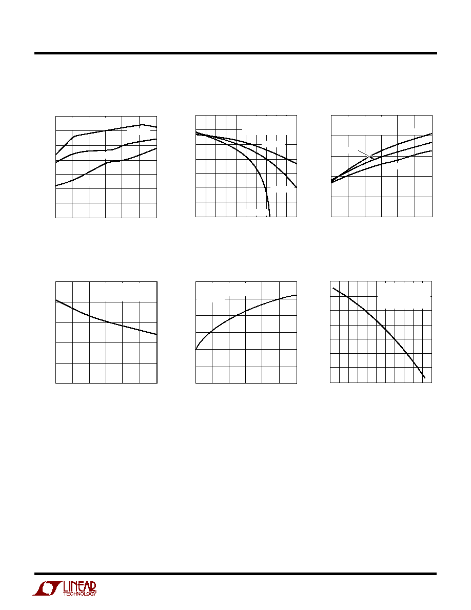
TYPICAL PERFOR A CE CHARACTERISTICS
U
W
SUPPLY VOLTAGE (V)
2.7
0.640
0.635
0.630
0.625
0.620
0.615
0.610
0.605
3.6
4.2
3201 G01
3.0
3.3
3.9
4.5
FEEDBACK VOLTAGE (V)
C
FLY
= C
FILTER
= O.22
µ
F
C
IN
= C
OUT
= 1
µ
F
T
A
= 85
°
C
T
A
= 40
°
C
T
A
= 25
°
C
LOAD CURRENT (mA)
0
4.15
4.10
4.05
4.00
3.95
3.90
3.85
3.80
3201 G02
20 40 60 80 100 120 140 160 180 200
OUTPUT VOLTAGE (V)
C
FLY
= C
FILTER
= O.22
µ
F
C
IN
= C
OUT
= 1
µ
F
T
A
= 25
°
C
V
IN
= 4.5V
V
IN
= 3.2V
V
IN
= 2.7V
SUPPLY VOLTAGE (V)
2.7
OSCILLATOR FREQUENCY (MHz)
2.2
2.0
1.8
1.6
1.4
1.2
3.3
3.9
4.2
3201 G03
3.0
3.6
4.5
C
FLY
= C
FILTER
= O.22
µ
F
C
IN
= C
OUT
= 1
µ
F
V
OUT
= 4V
T
A
= 85
°
C
T
A
= 40
°
C
T
A
= 25
°
C
SUPPLY VOLTAGE (V)
2.7
SHORT-CIRCUIT CURRENT (mA)
250
200
150
100
50
0
3.3
3.9
4.2
3201 G04
3.0
3.6
4.5
C
FLY
= C
FILTER
= O.22
µ
F
C
IN
= C
OUT
= 1
µ
F
T
A
= 25
°
C
FEEDBACK VOLTAGE (V)
0.620
0.615
0.610
0.605
0.600
0.595
0.590
C
FLY
= C
FILTER
= O.22
µ
F
C
IN
= C
OUT
= 1
µ
F
T
A
= 25
°
C
SUPPLY VOLTAGE (V)
2.7
3.3
3.9
4.2
3201 G05
3.0
3.6
4.5
Feedback Voltage vs Supply
Voltage
Oscillator Frequency vs Supply
Voltage
Feedback Voltage
vs Supply Voltage
I
OUT
= 100mA, V
OUT
= 4V
Output Voltage vs Load Current
Short-Circuit Current vs Supply
Voltage
Feedback Voltage vs I
OUT
I
OUT
(mA)
0
V
FB
(V)
0.64
0.62
0.60
0.58
0.56
0.54
0.52
0.50
20
3201 G06
40 60 80 100 120 140 160 180 200 220
C
FLY
= C
FILTER
= 0.22
µ
F
C
IN
= C
OUT
= 1
µ
F
T
A
= 25
°
C
V
IN
= 3.6V
LTC3201
4
3201f
U
U
U
PI FU CTIO S
V
OUT
(Pin 1): Charge Pump Output. Bypass with a 1
µ
F
ceramic capacitor to GND.
CP (Pin 2): Flying Capacitor Positive Terminal.
FILTER (Pin 3): Input Noise Filter Terminal. Bypass with a
0.22
µ
F high resonant frequency ceramic capacitor to
GND. Place filter capacitor less than 1/8" from device.
CM (Pin 4): Flying Capacitor Negative Terminal.
GND (Pin 5): Ground. Connect to a ground plane for best
performance.
D0 (Pin 6): Current Control DAC LSB Input.
D1 (Pin 7): Current Control DAC Bit 1 Input.
D2 (Pin 8): Current Control DAC MSB Input. Inputs D0 to
D2 program a 3-bit DAC output which is used as the
internal reference voltage. The DAC output reference volt-
age is used to regulate amount of current flowing through
the LEDs. An internal control loop adjusts the charge
pump output such that the voltage drop across an external
sense resistor connected from FB to GND equals the
internal DAC output reference voltage. See Truth Table in
Applications Information section for internal reference
settings vs DAC code. When D0 to D2 are low, the part
enters a low current shutdown mode and the load is
disconnected from V
IN
.
V
IN
(Pin 9): Input Voltage. V
IN
may be between 2.7V and
4.5V. Bypass V
IN
with a 1
µ
F low ESR capacitor to ground.
FB (Pin 10): Charge Pump Feedback Input. This pin acts
as a sense pin for I
OUT
. Connect a sense resistor between
FB and GND to set the output current. I
OUT
will be adjusted
until V
FB
= internal DAC output reference.
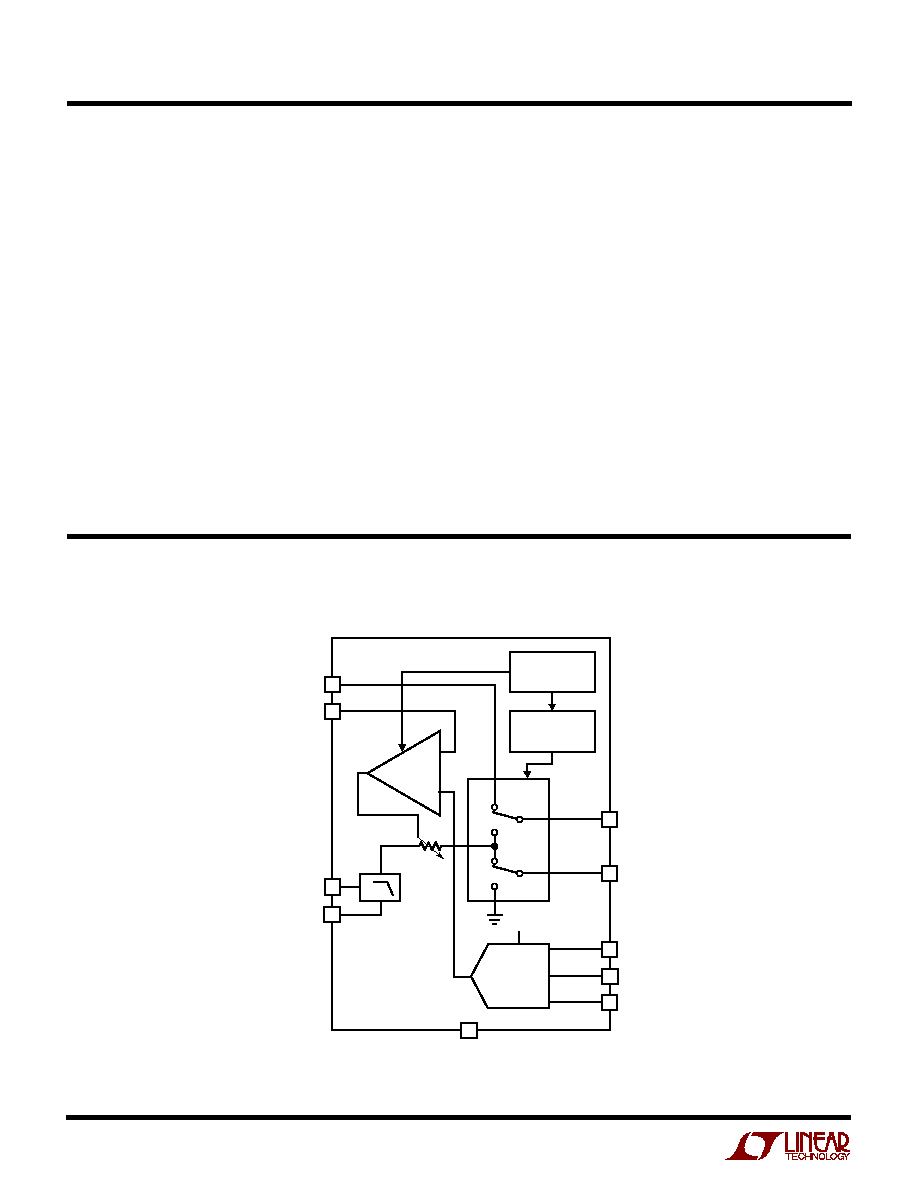
SI PLIFIED
W
BLOCK DIAGRA
W
+
3201 BD
CHARGE
PUMP
3-BIT
DAC
LPF
3
1
10
9
5
2
4
8
7
6
SOFT-START
AND
SWITCH CONTROL
1.8MHz
OSCILLATOR
GND
FILTER
V
IN
V
OUT
FB
CP
CM
D1
D2
D0
1.2V
LTC3201
5
3201f
APPLICATIO S I FOR ATIO
W
U
U
U
Operation (Refer to Simplified Block Diagram)
The LTC3201 is a switched capacitor boost charge pump
especially designed to drive white LEDs in backlighting
applications. The LTC3201's internal regulation loop
maintains constant LED output current by monitoring the
voltage at the FB pin. The device has a novel internal filter
that, along with an external 0.22
µ
F capacitor, significantly
reduces input current ripple. An internal 7-state DAC
allows the user to lower the regulation voltage at the FB
pin, thus lowering the LED current. To regulate the output
current, the user places a sense resistor between FB and
GND. The white LED is then placed between V
OUT
and FB.
The value at the FB pin is then compared to the output of
the DAC. The charge pump output voltage is then changed
to equalize the DAC output and the FB pin. The value of the
sense resistor determines the maximum value of the
output current.
When the charge pump is enabled, a two-phase
nonoverlapping clock activates the charge pump switches.
The flying capacitor is charged to V
IN
on phase one of the
clock. On phase two of the clock, it is stacked in series with
V
IN
and connected to V
OUT
. This sequence of charging and
discharging the flying capacitor continues at a free run-
ning frequency of 1.8MHz (typ) until the FB pin voltage
reaches the value of the DAC.
In shutdown mode all circuitry is turned off and the
LTC3201 draws only leakage current (<1
µ
A) from the V
IN
supply. Furthermore, V
OUT
is disconnected from V
IN
. The
LTC3201 is in shutdown when a logic low is applied to all
three D0:D2 pins. Note that if V
OUT
floats to >1.5V,
shutdown current will increase to 10
µ
A max. In normal
operation, the quiescent supply current of the LTC3201
will be slightly higher if any of the D0:D2 pins is driven high
with a signal that is below V
IN
than if it is driven all the way
to V
IN
. Since the D0:D2 pins are high impedance CMOS
inputs, they should never be allowed to float.
Input Current Ripple
The LTC3201 is designed to minimize the current ripple at
V
IN
. Typical charge pump boost converters draw large
amounts of current from V
IN
during both phase 1 and
phase 2 of the clocking. If there is a large nonoverlap time
between the two phases, the current being drawn from V
IN
can go down to zero during this time. At the full load of
100mA at the output, this means that the input could
potentially go from 200mA down to 0mA during the
nonoverlap time. The LTC3201 mitigates this problem by
minimizing the nonoverlap time, using a high (1.8MHz)
frequency clock, and employing a novel noise FILTER
network. The noise filter consists of internal circuitry plus
external capacitors at the FILTER and V
IN
pins. The filter
capacitor serves to cancel the higher frequency compo-
nents of the noise, while the V
IN
capacitor cancels out the
lower frequency components. The recommended values
are 0.22
µ
F for the FILTER capacitor and 1
µ
F for the V
IN
capacitor. Note that these capacitors must be of the highest
possible resonant frequencies. See Layout Considerations.
3-Bit DAC for Output Current Control
Digital pins D0, D1, D2 are used to control the output
current level. D0 = D1 = D2 = V
IN
allows the user to program
an output LED current that is equal to 0.63V/R
SENSE
, where
R
SENSE
is the resistor connected to any single LED and
connected between FB and ground. Due to the finite
transconductance of the regulation loop, for a given diode
setting, the voltage at the FB Pin will decrease as output
current increases. All LEDs subsequently connected in
parallel should then have similar currents. The mismatch-
ing of the LED V
F
and the mismatching of the sense
resistors will cause a differential current error between
LEDs connected to the same output. Once the sense
resistor is selected, the user can then control the voltage
applied across that resistor by changing the digital values
at D0:D2. This in turn controls the current into the LED.
Note that there are only 7 available current states. The 8th
is reserved to shutdown. This is the all 0s code. Refer to
Table below.
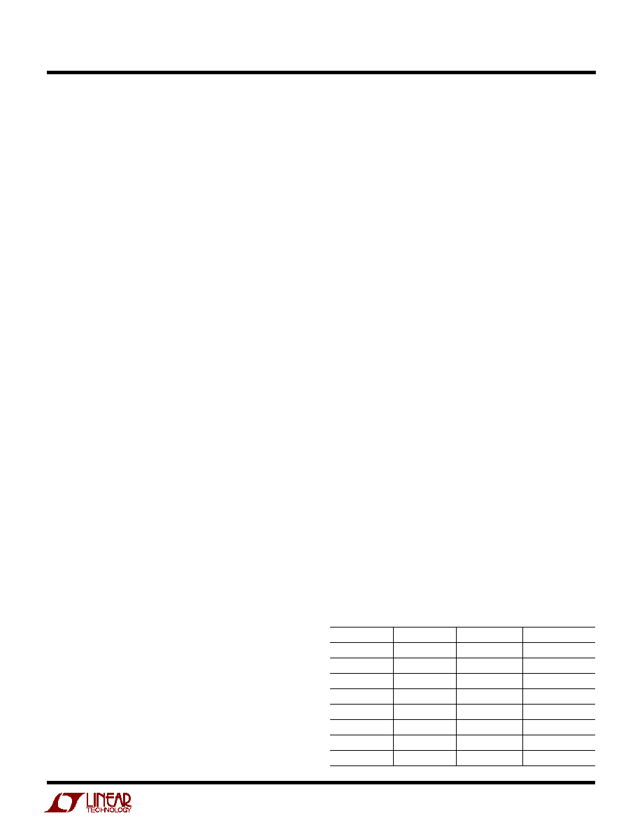
D0
D1
D2
FB
HIGH
HIGH
HIGH
0.63V
HIGH
HIGH
LOW
0.54V
HIGH
LOW
HIGH
0.45V
HIGH
LOW
LOW
0.36V
LOW
HIGH
HIGH
0.27V
LOW
HIGH
LOW
0.18V
LOW
LOW
HIGH
0.09V
LOW
LOW
LOW
Shutdown