Äîêóìåíòàöèÿ è îïèñàíèÿ www.docs.chipfind.ru
1
LTC3403
3403f
APPLICATIO S
U
TYPICAL APPLICATIO
U
s
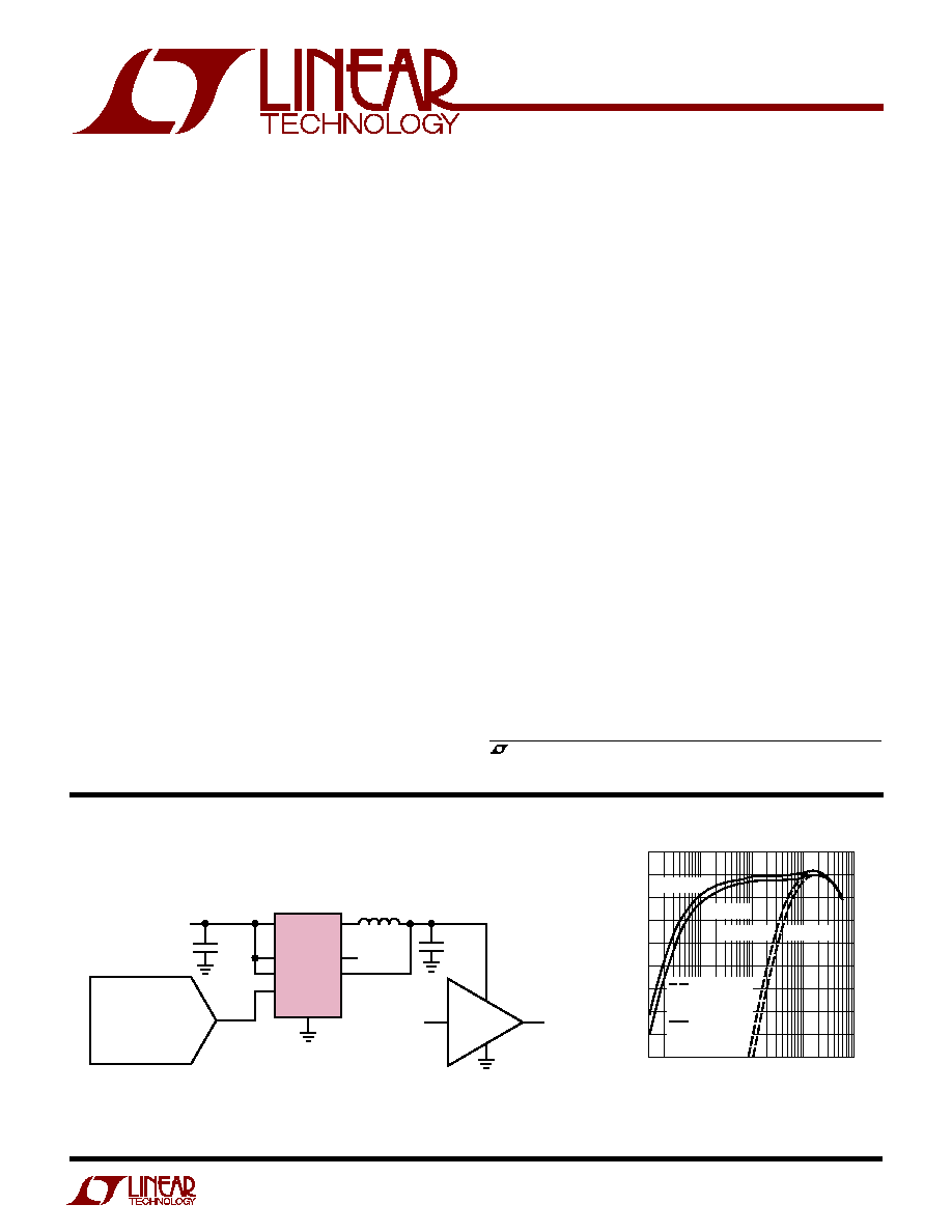
WCDMA Cell Phone Power Amplifiers
s
Wireless Modems
Figure 1a. WCDMA Transmitter Power Supply
Figure 1b. Efficiency vs Output Current
, LTC and LT are registered trademarks of Linear Technology Corporation.
Burst Mode is a registered trademark of Linear Technology Corporation.
V
IN
C
IN
10
µ
F
CER
V
IN
2.7V
TO 5V
*
**
LTC3403
RUN
REF
2.2
µ
H*
3403 F01a
MURATA LQH32CN2R2M11
TAIYO YUDEN JMK212BJ475MG
TAIYO YUDEN JMK212BJ106MN
3
SW
MODE
GDR
V
OUT
GND
C
OUT
**
4.7
µ
F
CER
V
OUT
3
×
V
REF
600mA
WCDMA
RF PA
OUTPUT
PROGRAMMING
DAC
OUTPUT CURRENT (mA)
60
EFFICIENCY (%)
70
75
85
95
0.1
10
100
1000
3403 F01b
50
1
80
65
55
90
V
IN
= 3.6V
V
IN
= 3.6V
V
IN
= 4.2V
V
IN
= 4.2V
FORCED
CONTINUOUS
MODE
Burst Mode
OPERATION
V
OUT
= 1.8V
1.5MHz, 600mA
Synchronous Step-Down
Regulator with Bypass Transistor
DESCRIPTIO
U
FEATURES
s
Dynamically Adjustable Output from 0.3V to 3.5V
s
Very Low Quiescent Current: Only 20
µ
A
During Operation
s
600mA Output Current
s
Internal P-Channel MOSFET Bypass Transistor
s
High Efficiency: Up to 96%
s
1.5MHz Constant Frequency Operation
s
No Schottky Diode Required
s
Low Dropout Operation: 100% Duty Cycle
s
2.5V to 5V Input Voltage Range
s
Drives Optional External P-Channel MOSFET
s
Shutdown Mode Draws < 1
µ
A Supply Current
s
Current Mode Operation for Excellent Line and
Load Transient Response
s
Overtemperature Protected
s
Available in 8-Lead 3mm
×
3mm DFN Package
The LTC
®
3403 is a high efficiency monolithic synchro-
nous buck regulator optimized for WCDMA power ampli-
fier applications. The output voltage can be dynamically
programmed from 0.3V to 3.5V. At V
OUT
> 3.6V an internal
bypass P-channel MOSFET connects V
OUT
directly to V
IN
,
eliminating power loss through the inductor. Selectable
forced continuous mode enables fast V
OUT
response to the
controlling input.
Supply current is only 20
µ
A in Burst Mode
®
operation and
drops to <1
µ
A in shutdown. The 2.5V to 5V input voltage
range makes the LTC3403 ideally suited for single Li-Ion
battery-powered applications. 100% duty cycle provides
low dropout operation, extending battery life in portable
systems.
Switching frequency is internally set at 1.5MHz, allowing
the use of small surface mount inductors and capacitors.
The internal synchronous switch increases efficiency and
eliminates the need for an external Schottky diode.
The LTC3403 is available in a low profile 8-lead 3mm
×
3mm DFN package.
2
LTC3403
3403f
SYMBOL
PARAMETER
CONDITIONS
MIN
TYP
MAX
UNITS
V
OUT
Regulated Output Voltage
V
REF
= 1.1V, MODE = V
IN
q
3.23
3.3
3.37
V
V
REF
= 0.1V, MODE = V
IN
q
0.25
0.3
0.35
V
V
OUT
Output Voltage Line Regulation
V
IN
= 2.5V to 5V
q
0.1
0.4
%/V
I
PK
Peak Inductor Current
V
IN
= 3V, V
REF
= 0.9V
0.70
1
1.25
A
V
LOADREG
Output Voltage Load Regulation
0.7
%
V
IN
Input Voltage Range
q
2.5
5
V
I
S
Input DC Operating Current
Burst Mode Operation
MODE = 0V, SW = Open
20
35
µ
A
Forced Continuous Mode Operation
MODE = V
IN
, SW = Open
1.5
2.5
mA
Shutdown
V
RUN
= 0V, V
IN
= 4.2V
0.1
1
µ
A
f
OSC
Oscillator Frequency
V
REF
0.25V
q
1.2
1.5
1.8
MHz
V
REF
0.1V
550
700
850
kHz
V
REF
Bypass PFET Turn-Off Threshold
V
REF
=
1.167
1.2
V
Bypass PFET Turn-On Threshold
V
REF
=
1.21
1.26
V
R
PFET
R
DS(ON)
of P-Channel FET
I
SW
= 160mA, Wafer Level
0.3
0.4
I
SW
= 160mA, DD Package
0.4
R
NFET
R
DS(ON)
of N-Channel FET
I
SW
= 160mA, Wafer Level
0.3
0.4
I
SW
= 160mA, DD Package
0.4
R
BYPASS
R
DS(ON)
of Bypass P-Channel FET
I
OUT
= 100mA, V
IN
= 3V, Wafer Level
0.15
0.18
I
OUT
= 100mA, V
IN
= 3V, DD Package (Note 4)
0.20
I
LSW
SW Leakage
V
RUN
= 0V, V
SW
= 0V or 5V, V
IN
= 5V
±
0.01
±
1
µ
A
I
LBYP
Bypass PFET Leakage
V
OUT
= 0V, V
IN
= 5V, V
REF
= 0V
±
0.01
±
1
µ
A
V
RUN
RUN Threshold
q
0.3
1
1.5
V
I
RUN
RUN Input Current
V
RUN
= 2.5V or 0V
q
±
0.01
±
1
µ
A
V
MODE
MODE Threshold
q
0.3
1.5
2
V
I
MODE
MODE Input Current
q
±
0.01
±
1
µ
A
I
REF
REF Input Current
q
±
0.01
±
1
µ
A
Input Supply Voltage (< 300
µ
s) .................. 0.3V to 6V
Input Supply Voltage (DC) ....................... 0.3V to 5.5V
RUN, REF, MODE, V
OUT
, GDR Voltages ..... 0.3V to V
IN
SW Voltage .................................. 0.3V to (V
IN
+ 0.3V)
P-Channel Switch Source Current (DC) ............. 800mA
N-Channel Switch Sink Current (DC) ................. 800mA
Peak SW Sink and Source Current ........................ 1.3A
Bypass P-Channel FET Source Current ...................... 1A
Operating Temperature Range (Note 2) .. 40
°
C to 85
°
C
Junction Temperature (Note 3) ............................ 125
°
C
Storage Temperature Range ................ 65
°
C to 150
°
C
(DD Package) .................................... 65
°
C to 125
°
C
Consult LTC Marketing for parts specified with wider operating temperature ranges.
ABSOLUTE AXI U RATI GS
W
W
W
U
PACKAGE/ORDER I FOR ATIO
U
U
W
(Note 1)
LTC3403EDD
ORDER PART
NUMBER
DD PART MARKING
LAAX
T
JMAX
= 125
°
C,
JA
= 43
°
C/ W,
JC
= 3
°
C/ W
The
q
denotes specifications which apply over the full operating temperature range, otherwise specifications are T
A
= 25
°
C.
V
IN
= 3.6V unless otherwise specified.
ELECTRICAL CHARACTERISTICS
8
7
6
5
1
2
3
4
V
OUT
REF
MODE
RUN
GDR
V
IN
GND
SW
TOP VIEW
DD PACKAGE
8-LEAD (3mm
×
3mm) PLASTIC DFN
EXPOSED PAD IS GND (PIN 9)
MUST BE SOLDERED TO PCB
9
3
LTC3403
3403f
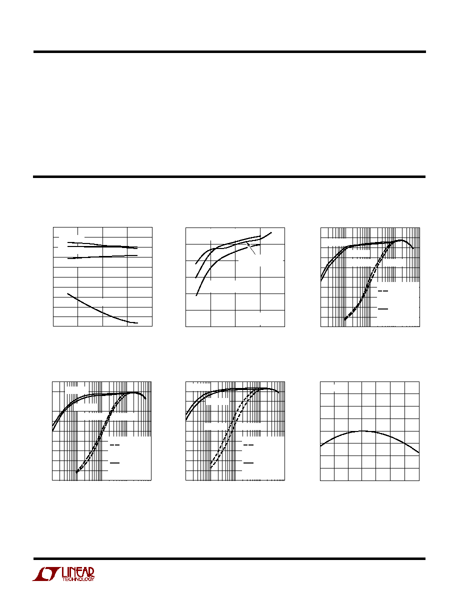
TYPICAL PERFOR A CE CHARACTERISTICS
U
W
Efficiency vs V
IN
Efficiency vs Output Current
Efficiency vs Output Current
Efficiency vs Output Current
Oscillator Frequency
vs Temperature
(From Figure 1a)
OUTPUT CURRENT (mA)
30
EFFICIENCY (%)
90
100
20
10
80
50
70
60
40
0.1
10
100
1000
3403 G02
0
1
V
IN
= 3.6V
V
IN
= 3.6V
V
IN
= 4.2V
V
IN
= 4.2V
T
A
= 25
°
C
FORCED
CONTINUOUS
MODE
Burst Mode
OPERATION
V
OUT
= 1.2V
OUTPUT CURRENT (mA)
30
EFFICIENCY (%)
90
100
20
10
80
50
70
60
40
0.1
10
100
1000
3403 G03
0
1
V
IN
= 3.6V
V
IN
= 3.6V
V
IN
= 4.2V
V
IN
= 4.2V
T
A
= 25
°
C
FORCED
CONTINUOUS
MODE
Burst Mode
OPERATION
V
OUT
= 1.5V
TEMPERATURE (
°
C)
50
FREQUENCY (MHz)
1.70
1.65
1.60
1.55
1.50
1.45
1.40
1.35
1.30
25
75
25
0
50
100
125
V
IN
= 3.6V
3403 G05
V
IN
(V)
2.5
EFFICIENCY (%)
55
50
65
70
75
100
85
3.0
3.5
3403 G01
60
90
95
80
4.0
4.5
I
L
= 300mA
I
L
= 600mA
I
L
= 100mA
I
L
= 10mA
OUTPUT CURRENT (mA)
30
EFFICIENCY (%)
90
100
20
10
80
50
70
60
40
0.1
10
100
1000
3403 G04
0
1
V
IN
= 3.6V
V
IN
= 3.6V
V
IN
= 4.2V
V
IN
= 4.2V
T
A
= 25
°
C
FORCED
CONTINUOUS
MODE
Burst Mode
OPERATION
V
OUT
= 2.5V
Note 1: Absolute Maximum Ratings are those values beyond which the life
of a device may be impaired.
Note 2: The LTC3403E is guaranteed to meet performance specifications
from 0
°
C to 70
°
C. Specifications over the 40
°
C to 85
°
C operating
temperature range are assured by design, characterization and correlation
with statistical process controls.
Note 3: T
J
is calculated from the ambient temperature T
A
and power
dissipation P
D
according to the following formula:
LTC3403: T
J
= T
A
+ (P
D
)(43
°
C/W)
Note 4: When V
REF
> 1.2V and V
REF
x3 > V
IN
, the P-channel FET will be on
in parallel with the bypass PFET reducing the overall R
DS(ON)
.
Note 5: This IC includes overtemperature protection that is intended to
protect the device during momentary overload conditions. Junction
temperature will exceed 125
°
C when overtemperature protection is active.
Continuous operation above the specified maximum operating junction
temperature may impair device reliability.
ELECTRICAL CHARACTERISTICS
V
OUT
(V)
0
EFFICIENCY (%)
100
90
80
70
60
50
40
1
2
3
4
3403 GO1a
T
A
= 25
°
C
V
IN
= 3.6V
100mA BURST
MODE 0PERATION
600mA FORCED
CONTINUOUS MODE
100mA FORCED
CONTINUOUS MODE
Efficiency vs V
OUT
4
LTC3403
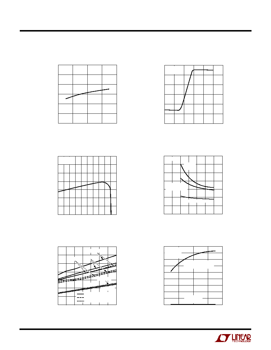
3403f
Output Voltage vs Load Current
R
DS(ON)
vs Input Voltage
LOAD CURRENT (mA)
0
OUTPUT VOLTAGE (V)
1.844
1.834
1.824
1.814
1.804
1.794
1.784
1.774
100
500
700
3403 G07
400
900 1000
200 300
600
800
T
A
= 25
°
C
V
IN
= 3.6V
INPUT VOLTAGE (V)
1
0
0.4
0.5
0.7
4
6
3403 G08
0.3
0.2
2
3
5
7
0.1
0
0.6
R
DS(ON)
(
)
MAIN
SWITCH
SYNCHRONOUS
SWITCH
BYPASS SWITCH
T
A
= 25
°
C
R
DS(ON)
vs Temperature
TEMPERATURE (
°
C)
50
0.4
0.5
0.7
25
75
3403 G09
0.3
0.2
25
0
50
100
125
0.1
0
0.6
R
DS(ON)
(
)
MAIN SWITCH
SYNCHRONOUS SWITCH
BYPASS SWITCH
V
IN
= 2.7V
V
IN
= 3.6V
V
IN
= 3V
V
IN
= 4.2V
V
IN
= 4.2V
V
IN
= 3.6V
Oscillator Frequency
vs Supply Voltage
SUPPLY VOLTAGE (V)
2
OSCILLATOR FREQUENCY (MHz)
1.8
1.7
1.6
1.5
1.4
1.3
1.2
3
4
5
6
3403 G06
T
A
= 25
°
C
Dynamic Supply Current
vs Supply Voltage
SUPPLY VOLTAGE (V)
2
DYNAMIC SUPPLY CURRENT (
µ
A)
2500
3000
3500
6
3403 G10
2000
1500
0
3
4
5
1000
500
4500
4000
T
A
= 25
°
C
V
OUT
= 1.8V
I
LOAD
= 0A
FORCED CONTINUOUS
MODE
Burst Mode
OPERATION
(From Figure 1a)
V
OUT
(V)
0
FREQUENCY (kHz)
1600
1400
1200
1000
800
600
400
0.2
0.4
0.6
0.8
3403 F06a
1.0
1.2
T
A
= 25
°
C
V
IN
= 3.6V
TYPICAL PERFOR A CE CHARACTERISTICS
U
W
Frequency vs V
OUT
5
LTC3403
3403f
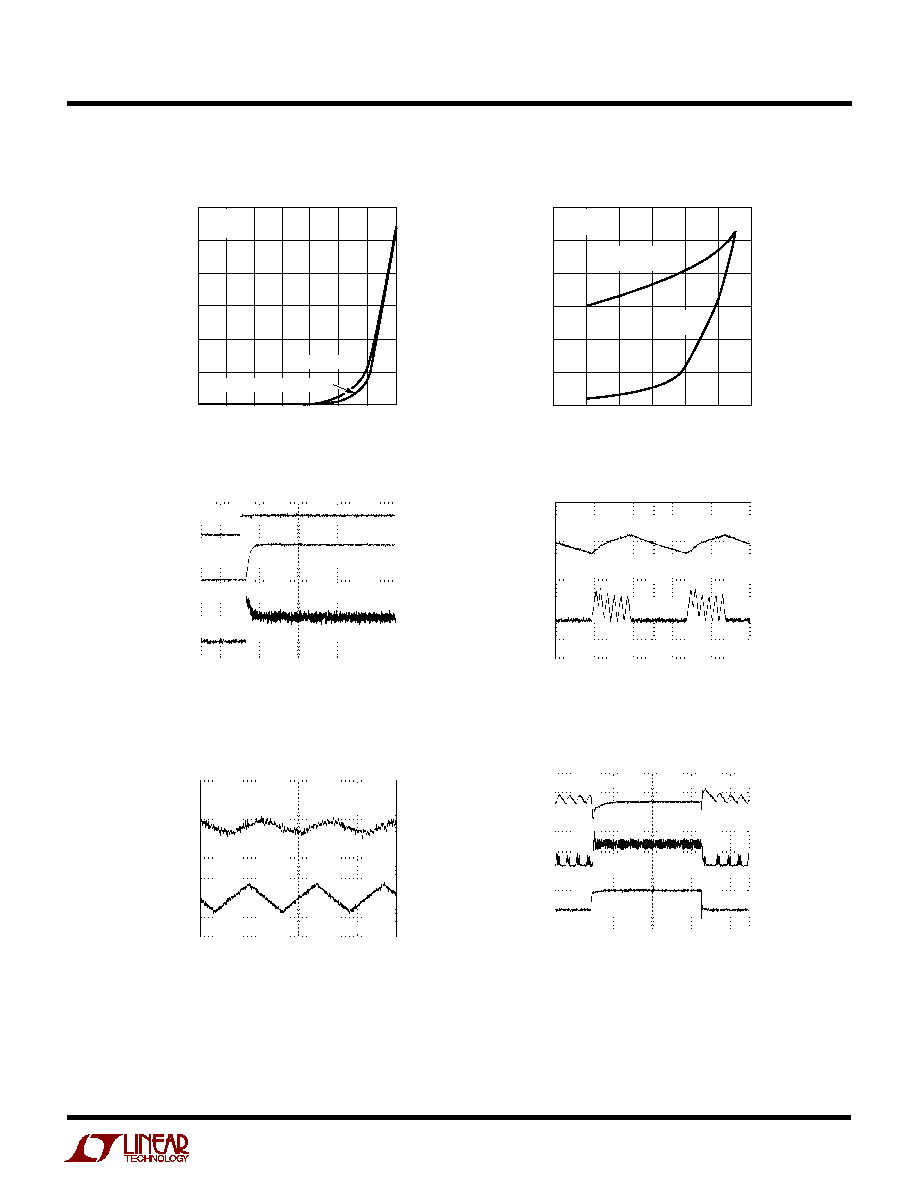
Switch Leakage vs Temperature
Switch Leakage vs Input Voltage
TEMPERATURE (
°
C)
50
SWITCH LEAKAGE (nA)
200
250
300
25
75
3403 G11
150
100
25
0
50
100
125
50
0
V
IN
= 5.5V
RUN = 0V
MAIN SWITCH
SYNCHRONOUS SWITCH
INPUT VOLTAGE (V)
0
0
SWITCH LEAKAGE (pA)
20
40
60
80
120
1
2
3
4
3403 G12
5
6
100
T
A
= 25
°
C
RUN = 0V
SYNCHRONOUS
SWITCH
MAIN
SWITCH
RUN
2V/DIV
V
OUT
1V/DIV
I
L
500mA/DIV
40
µ
s/DIV
V
IN
= 3.6V
V
REF
= 0.6V
R
LOAD
= 3
MODE = 3.6V, FORCED CONTINUOUS MODE
3403 G13
Start-Up from Shutdown
Burst Mode Operation
Load Step Response
V
IN
= 3.6V
V
REF
= 0.6V
I
LOAD
= 60mA
MODE = 0V
V
OUT
0.1V/DIV
I
L
200mA/DIV
2
µ
s/DIV
3403 G14
V
OUT
10mV/DIV
I
L
200mA/DIV
200ns/DIV
V
IN
= 3.6V
V
REF
= 0.6V
I
LOAD
= 0A
MODE = 3.6V
3403 G15
V
OUT
200mV/DIV
I
L
500mA/DIV
I
LOAD
500mA/DIV
20
µ
s/DIV
V
IN
= 3.6V
V
REF
= 0.6V
I
LOAD
= 50mA TO 600mA
MODE = 0V, Burst Mode OPERATION
3403 G16
Forced Continuous Mode
TYPICAL PERFOR A CE CHARACTERISTICS
U
W
(From Figure 1a)