 | –≠–ª–µ–∫—Ç—Ä–æ–Ω–Ω—ã–π –∫–æ–º–ø–æ–Ω–µ–Ω—Ç: LTC3404 | –°–∫–∞—á–∞—Ç—å:  PDF PDF  ZIP ZIP |
1
LTC3409
3409f
Cellular Phones
Digital Cameras
MP3 Players
High Efficiency Step-Down Converter
600mA Low V
IN
Buck
Regulator in 3mm ◊ 3mm DFN
1.6V to 5.5V Input Voltage Range
Internal Soft-Start
Selectable 1.7MHz or 2.6MHz Constant Frequency
Operation
Internal Oscillator can be Synchronizable to an
External Clock, 1MHz to 3MHz Range
High Efficiency: Up to 95%
Very Low Quiescent Current: Only 65µA During
Burst Mode
Æ
Operation
600mA Output Current (V
IN
= 1.8V, V
OUT
= 1.2V)
750mA Peak Inductor Current
No Schottky Diode Required
Low Dropout Operation: 100% Duty Cycle
0.613V Reference Voltage
Stable with Ceramic Capacitors
Shutdown Mode Draws <1µA Supply Current
Current Mode Operation for Excellent Line and Load
Transient Response
Overtemperature Protection
Available in a Low Profile (0.75mm) 8-Lead
(3mm ◊ 3mm) DFN Package
Burst Mode Efficiency, 1.8V
OUT
FEATURES
DESCRIPTIO
U
APPLICATIO S
U
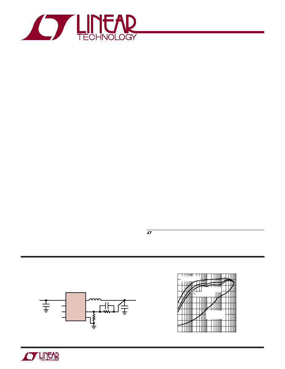
TYPICAL APPLICATIO
U
The LTC
Æ
3409 is a high efficiency, monolithic synchro-
nous buck regulator using a constant frequency, current
mode architecture. The output voltage is adjusted via an
external resistor divider.
Fixed switching frequencies of 1.7MHz and 2.6MHz are
supported. Alternatively, an internal PLL will synchronize
to an external clock in the frequency range of 1MHz to
3MHz. This range of switching frequencies allows the use
of small surface mount inductors and capacitors, includ-
ing ceramics.
Supply current during Burst Mode operation is only 65µA
dropping to <1µA in shutdown. The 1.6V to 5.5V input
voltage range makes the LTC3409 ideally suited for single
cell Li-Ion, Li-Metal and 2-cell alkaline, NiCd or NiMH
battery-powered applications. 100% duty cycle capability
provides low dropout operation, extending battery life in
portable systems. Burst Mode operation can be user-
enabled, increasing efficiency at light loads, further ex-
tending battery life.
The internal synchronous switch increases efficiency and
eliminates the need for an external Schottky diode. Inter-
nal soft-start offers controlled output voltage rise time at
start-up without the need for external components.
V
IN
RUN
MODE
SYNC
SW
V
FB
GND
LTC3409
2.2µH*
V
OUT
1.8V
255k
4.7µF
CER
V
IN
1.8V TO 5.5V
133k
*SUMIDA CDRH2D18/LD
3409 TA01
10pF
10µF
CER
, LTC and LT are registered trademarks of Linear Technology Corporation.
Burst Mode is a registered trademark of Linear Technology Corporation.
All other trademarks are the property of their respective owners.
Protected by U.S. Patents, including 5481178, 6580258, 6304066, 6127815,
6498466, 6611131.
LOAD CURRENT (mA)
30
EFFICIENCY (%)
POWER LOSS (W)
90
100
20
10
80
50
70
60
40
0.1
10
100
1000
3409 TA01b
0
1.0
0.1
0
1
2.5V
IN
, BURST
4.2V
IN
, BURST
3.6V
IN
, BURST
POWER LOST
3.6V
IN
, BURST

2
LTC3409
3409f
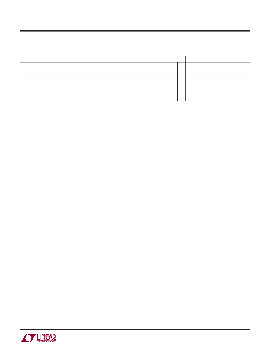
SYMBOL
PARAMETER
CONDITIONS
MIN
TYP
MAX
UNITS
V
RUN
RUN Threshold
0.3
0.65
1.1
V
I
RUN
RUN Leakage Current
0.01
1
µA
V
MODE
MODE Threshold
0.3
0.65
1.1
V
I
MODE
MODE Leakage Current
0.01
1
µA
V
SYNCTH
SYNC Threshold
0.3
0.65
1.1
V
I
SYNC
SYNC Leakage Current
0.01
1
µA
V
FB
Regulated Feedback Voltage
(Note 4) T
A
= 25∞C
0.6007
0.6130
0.6252
V
(Note 4) 0∞C T
A
85∞C
0.5992
0.6130
0.6268
V
(Note 4) ≠40∞C T
A
85∞C
0.5977
0.6130
0.6283
V
I
VFB
Feedback Current
±30
nA
V
OVL
V
FBOVL
Overvoltage Lockout
V
OVL
= V
FBOVL
≠ V
FB
(Note 6)
35
61
85
mV
V
FB
Reference Voltage Line Regulation
(Note 4)
0.04
0.4
%/V
V
OUT
Output Voltage Line Regulation
I
OUT
= 100mA, 1.6V < V
IN
< 5.5V
0.04
0.4
%/V
I
PK
Peak Inductor Current
V
IN
= 2.2V, V
FB
= 0.5V or V
OUT
= 90%,
0.75
1
1.3
A
Duty Cycle < 35%
V
LOADREG
Output Voltage Load Regulation
0.5
%
V
IN
Input Voltage Range
1.6
5.5
V
I
S
Input DC Bias Current
(Note 5)
Active Mode
V
OUT
= 90%, I
LOAD
= 0A
350
475
µA
Sleep Mode
V
OUT
= 103%, I
LOAD
= 0A
65
120
µA
Shutdown
V
RUN
= 0V, V
IN
= 5.5V
0.1
5
µA
f
OSC
Nominal Oscillator Frequency
SYNC = GND
0.9
1.7
2.1
MHz
SYNC = V
IN
1.8
2.6
3.0
MHz
SYNC TH
SYNC Threshold
When SYNC Input is Toggling (Note 7)
0.63
V
SYNC f
MIN
Minimum SYNC Pin Frequency
1
MHz
SYNC f
MAX
Maximum SYNC Pin Frequency
3
MHz
SYNC PW
Minimum SYNC Pulse Width
100
ns
t
SS
Soft-Start Period
RUN
1
ms
Input Supply Voltage .................................. ≠ 0.3V to 6V
RUN, V
FB
, MODE, SYNC Voltages . ≠ 0.3V to (V
IN
+ 0.3V)
SW Voltage ................................... ≠ 0.3V to (V
IN
+ 0.3V)
Operating Temperature Range (Note 2) .. ≠ 40∞C to 85∞C
Junction Temperature (Note 3) ............................ 125∞C
Storage Temperature Range ................ ≠ 65∞C to 125∞C
Consult LTC Marketing for parts specified with wider operating temperature ranges.
ABSOLUTE AXI U RATI GS
W
W
W
U
PACKAGE/ORDER I FOR ATIO
U
U
W
(Note 1)
LTC3409EDD
ORDER PART
NUMBER
DD PART MARKING
LBNM
T
JMAX
= 125∞C,
JA
= 43∞C/ W
EXPOSED PAD (PIN 9) IS GND
MUST BE SOLDERED TO PCB
The
denotes specifications which apply over the full operating temperature range, otherwise specifications are T
A
= 25∞C.
V
IN
= 2.2V unless otherwise specified.
ELECTRICAL CHARACTERISTICS
TOP VIEW
9
DD PACKAGE
8-LEAD (3mm ◊ 3mm) PLASTIC DFN
5
6
7
8
4
3
2
1
V
FB
GND
V
IN
V
IN
SYNC
RUN
SW
MODE
3
LTC3409
3409f
SYMBOL
PARAMETER
CONDITIONS
MIN
TYP
MAX
UNITS
SYNC t
O
SYNC Timeout
Delay from Removal of EXT CLK Until Fixed
30
µs
Frequency Operation Begins (Note 7)
R
PFET
R
DS(ON)
of P-Channel FET
I
SW
= 100mA, Wafer Level
0.33
I
SW
= 100mA, DD Package
0.35
R
NFET
R
DS(ON)
of N-Channel FET
I
SW
= 100mA, Wafer Level
0.22
I
SW
= 100mA, DD Package
0.25
I
LSW
SW Leakage
V
RUN
= 0V, V
SW
= 0V or 5V, V
IN
= 5V
±0.1
±3
µA
The
denotes specifications which apply over the full operating temperature range, otherwise specifications are T
A
= 25∞C.
V
IN
= 2.2V unless otherwise specified.
ELECTRICAL CHARACTERISTICS
Note 1: Absolute Maximum Ratings are those values beyond which the life
of a device may be impaired.
Note 2: The LTC3409E is guaranteed to meet performance specifications
from 0∞C to 70∞C. Specifications over the ≠40∞C to 85∞C operating
temperature range are assured by design, characterization and correlation
with statistical process controls.
Note 3: T
J
is calculated from the ambient temperature T
A
and power
dissipation P
D
according to the following formula:
LTC3409: T
J
= T
A
+ (P
D
)(43∞C/W)
This IC includes overtemperature protection that is intended to protect the
device during momentary overload conditions. Overtemperature protection
becomes active at a junction temperature greater than the maximum
operating junction temperature. Continuous operation above the specified
maximum operating junction temperature may impair device reliability.
Note 4: The LTC3409 is tested in a proprietary test mode that connects
V
FB
to the output of the error amplifier.
Note 5: Dynamic supply current is higher due to the gate charge being
delivered at the switching frequency.
Note 6: V
OVL
is the amount V
FB
must exceed the regulated feedback
voltage.
Note 7: Determined by design, not production tested.
4
LTC3409
3409f
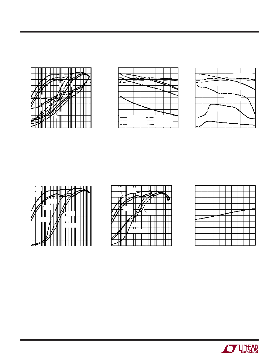
TYPICAL PERFOR A CE CHARACTERISTICS
U
W
Efficiency/Power Lost
vs Load Current, V
OUT
= 1.8V
Efficiency vs Input Voltage
V
OUT
= 1.2V, Pulse Skip
LOAD CURRENT (mA)
30
EFFICIENCY (%)
POWER LOSS (mW)
90
100
20
10
80
50
70
60
40
0.1
10
100
1000
3409 G01
0
0.1
1.0
1: 2.5V
IN
, BURST
2: 3.6V
IN
, BURST
3: 4.2V
IN
, BURST
4: 2.5V
IN
, PULSE SKIP
5: 3.6V
IN
, PULSE SKIP
6: 4.2V
IN
, PULSE SKIP
7: POWER LOST, 2.5V
IN
, BURST
8: POWER LOST, 2.5V
IN
, PULSE SKIP
9: POWER LOST, 3.6V
IN
, BURST
10: POWER LOST, 3.6V
IN
, PULSE SKIP
11: POWER LOST, 4.2V
IN
, BURST
12: POWER LOST, 4.2V
IN
, PULSE SKIP
0
1
1
2
3
6
9
5
4
12
8
7
10
11
INPUT VOLTAGE (V)
1.5
0
EFFICIENCY (%)
10
30
40
50
100
70
2.5
3.5
3409 G02
20
80
90
60
4.5
5.5
I
OUT
= 0.1mA
I
OUT
= 1mA
I
OUT
= 10mA
I
OUT
= 100mA
I
OUT
= 600mA
I
OUT
= 800mA
Efficiency vs Input Voltage
V
OUT
= 1.2V, Burst Mode Operation
INPUT VOLTAGE (V)
1.5
0
EFFICIENCY (%)
10
30
40
50
100
70
2.5
3.5
3409 G03
20
80
90
60
4.5
5.5
I
OUT
= 0.1mA
I
OUT
= 1mA
I
OUT
= 100mA
I
OUT
= 10mA
I
OUT
= 600mA
I
OUT
= 800mA
Efficiency vs Load Current
V
OUT
= 2.5V
Efficiency vs Load Current
V
OUT
= 1.2V
Reference Voltage
vs Temperature
LOAD CURRENT (mA)
30
EFFICIENCY (%)
90
100
20
10
80
50
70
60
40
0.1
10
100
1000
3409 G04
0
1
PULSE SKIP
BURST
2.7V
IN
2.7V
IN
4.2V
IN
4.2V
IN
3.6V
IN
3.6V
IN
LOAD CURRENT (mA)
30
EFFICIENCY (%)
90
100
20
10
80
50
70
60
40
0.1
10
100
1000
3409 G05
0
1
PULSE SKIP
BURST
1.6V
IN
1.6V
IN
3.1V
IN
3.1V
IN
2.5V
IN
2.5V
IN
TEMPERATURE (∞C)
≠50
REFERENCE VOLTAGE (V)
0.616
0.618
110
1011 G06
0.615
0.614
0.613
0.612
0.611
0.610
0.609
0.608
0.617
≠10
≠30
30
10
70 90
130
50
150
(From Typical Application on the front page except for the resistive divider resistor values)

5
LTC3409
3409f
Oscillator Frequency
vs Temperature
TEMPERATURE (∞C)
≠50
OSCILLATOR FREQUENCY (MHz)
2.10
2.40
2.70
2.60
2.50
2.20
2.30
1.90
2.00
1.60
1.70
1.30
1.40
25
75
125
100
3409 G07
1.80
1.50
1.20
≠25
0
50
V
IN
= 1.6V
V
IN
= 1.6V
V
IN
= 2.7V
V
IN
= 2.7V
OSC 2.6MHz
OSC 1.7MHz
V
IN
= 4.2V
V
IN
= 4.2V
INPUT VOLTAGE (V)
1.5
OSCILLATOR FREQUENCY SHIFT (%)
≠2
0
2
f
LOW
1.7MHz
f
HIGH
2.6MHz
5.5
3409 G08
≠4
≠6
≠10
2.5
3.5
4.5
≠8
6
4
LOAD CURRENT (mA)
0
1.18
OUTPUT VOLTAGE (V)
1.19
1.20
1.21
1.22
100 200 300 400
3409 G09
500 600 700 800 900
1.2V
OUT
BURST
1.2V
OUT
PULSE
SKIP
Oscillator Frequency Shift
vs Input Voltage
Output Voltage vs Load Current
V
IN
= 1.6V
R
DS(ON)
vs Input Voltage
Dynamic Supply Current
vs Input Voltage
INPUT VOLTAGE (V)
1.5
0
R
DS(0N)
(
)
0.050
0.150
0.200
0.250
3.5
5.5
0.450
3409 G10
0.100
2.5
4.5
0.300
0.350
0.400
MAIN
SWITCH
SYNCHRONOUS
SWITCH
R
DS(ON)
vs Input Temperature
TEMPERATURE (∞C)
≠50
0.35
0.40
1.6V
1.6V
2.7V
2.7V
4.2V
4.2V
0.50
0.55
25
75
3409 G11
0.30
0.25
≠25
0
50
100
125
0.20
0.15
0.10
0.45
R
DS(ON)
(
)
SYNCHRONOUS SWITCH
MAIN SWITCH
INPUT VOLTAGE (V)
1.5
0
DYNAMIC SUPPLY CURRENT, PULSE SKIP (
µ
A)
DYNAMIC SUPPLY CURRENT, BURST/SLEEP (
µ
A)
1000
3000
4000
5000
6000
2.5
3.5
4
6
3409 G12
2000
2
3
4.5
5
5.5
0
20
60
80
100
40
120
PULSE
SKIP
BURST/SLEEP
V
FB
= V
IN
V
FB
= 0
V
OUT
= 1.5V
I
OUT
= 0
V
OUT
= 1.5V
I
OUT
= 0
Dynamic Supply Current vs
Temperature, V
IN
= 3.6V,
V
OUT
= 1.5V, 0 Load
Switch Leakage vs Temperature
V
IN
= 5.5V
TEMPERATURE (∞C)
≠50
SWITCH LEAKAGE (nA)
4000
5000
6000
25
75
3409 G14
3000
2000
≠25
0
50
100
125
1000
0
MAIN SWITCH
V
IN
= 5.5V
SYNCHRONOUS SWITCH
Switch Leakage vs Input Voltage
INPUT VOLTAGE (V)
0
SWITCH LEAKAGE (nA)
25
30
35
8
3409 G15
20
15
0
2
4
6
10
5
45
40
MAIN SWITCH
SYNCHRONOUS
SWITCH
TEMPERATURE (∞C)
≠50
0
DYNAMIC SUPLLY CURRENT (
µ
A)
50
150
200
250
500
350
0
50
75
3409 G13
100
400
450
300
≠25
25
100
125
PULSE SKIP
BURST
TYPICAL PERFOR A CE CHARACTERISTICS
U
W
(From Typical Application on the front page except for the resistive divider resistor values)