 | –≠–ª–µ–∫—Ç—Ä–æ–Ω–Ω—ã–π –∫–æ–º–ø–æ–Ω–µ–Ω—Ç: LTC3406 | –°–∫–∞—á–∞—Ç—å:  PDF PDF  ZIP ZIP |
LTC3455
1
3455f
APPLICATIO S
U
FEATURES
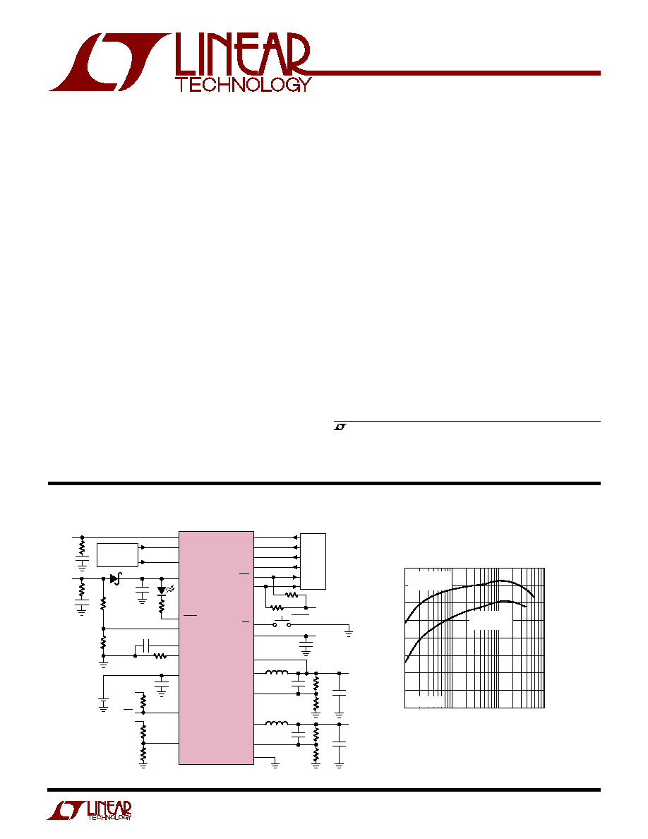
TYPICAL APPLICATIO
U
DESCRIPTIO
U
LOAD CURRENT (mA)
60
EFFICIENCY (%)
80
75
70
65
85
90
95
100
3455 TA01b
V
BAT
= 3.6V
SWITCHER 1
V
OUT1
= 1.8V
SWITCHER 2
V
OUT2
= 3.3V
1
10
100
1000
The LTC
Æ
3455 is a complete power management solution
for a variety of portable applications. The device contains
two synchronous step-down DC/DC converters, a USB
power controller, a full-featured Li-Ion battery charger, a
Hot Swap output, a low-battery indicator, and numerous
internal protection features. The LTC3455 provides a
small, simple solution for obtaining power from three
different power sources: a single-cell Li-Ion battery, a USB
port, and a wall adapter. Current drawn from the USB bus
is accurately limited under all conditions. Whenever a USB
or a wall adapter is present, the battery charger is enabled
and all internal power for the device is drawn from the
appropriate external power source. All outputs are dis-
charged to ground during shutdown to provide complete
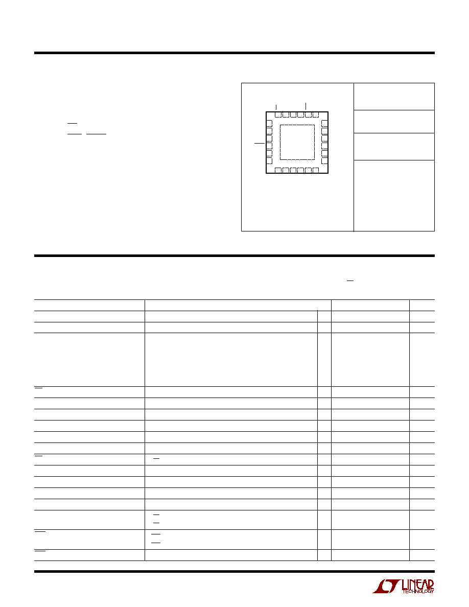
output disconnect. The device is available in a
4mm
◊
4mm 24-pin exposed-pad QFN package.
s
Handheld Computers
s
Digital Cameras
s
MP3 Players
, LTC and LT are registered trademarks of Linear Technology Corporation.
s
Seamless Transition between Input Power Sources:
Li-Ion Battery, USB, and 5V Wall Adapter
s
Accurate USB Current Limiting (500mA/100mA)
s
Two High Efficiency DC/DC Converters: Up to 96%
s
Thermal Regulation Maximizes Battery Charge
Rate without Risk of Overheating*
s
Full-Featured Li-Ion Battery Charger
s
Hot SwapTM Output for SDIO and Memory Cards
s
Pin-Selectable Burst Mode
Æ
Operation
s
Output Disconnect: All Outputs Discharged to
Ground During Shutdown
s
Available in a 4mm
◊
4mm
◊
0.8mm 24-Pin
QFN Package
Efficiency
Hot Swap is a trademark of Linear Technology Corporation.
Burst Mode is a registered trademark of Linear Technology Corporation.
*U.S. Patent 6,522,118
11
10
13
14
1
1
µ
F
1
µ
F
10
µ
F
4.7
µ
F
WALL 5V
3.3V, HS
8
6
5
9
1
4.7
µ
F
USB 5V
4
2
3
18
12
249k
4.7
µ
H
80.6k
10pF
10
µ
F
3.3V
0.5A
1
7
100k
4.7
µ
H
80.6k
10pF
10
µ
F
1.8V
0.4A
16
17
LBO
24
23
20
21
19
22
15
0.1
µ
F
1k
806k
1M
1.8V
V
BAT
2.49M
1M
2.49k
1M
1.8V
25
3455 TA01a
µ
C
USB
CONTROLLER
SINGLE
CELL Li-ION
3.3V TO 4.2V
1.24k
3.32k
ON/OFF
+
WALLFB
HSI
HSO
V
MAX
USB
SUSPEND
USBHP
SW2
FB2
SW1
FB1
TIMER
PROG
AI
AO
V
BAT
ON
GND
CHRG
PBSTAT
RST
MODE
LTC3455
ON2
PWRON
HSON
Dual DC/DC Converter
with USB Power Manager
and Li-Ion Battery Charger
LTC3455
2
3455f
V
BAT
, V
MAX
, USB Voltages ...........................≠ 0.3V to 6V
SW1, SW2 Voltages .................... ≠ 0.3V to (V
MAX
+0.3V)
TIMER Voltage ............................. ≠ 0.3V to (V
MAX
+0.3V)
PWRON, ON, ON2, HSON Voltages .............≠ 0.3V to 6V
PBSTAT, RST, CHRG, AO Voltages .............. ≠ 0.3V to 6V
HSI, HSO Voltages .......................................≠ 0.3V to 6V
MODE, USBHP, SUSPEND Voltages ............≠ 0.3V to 6V
WALLFB, AI, PROG Voltages .......................≠ 0.3V to 2V
FB1, FB2 Voltages ........................................≠ 0.3V to 2V
Junction Temperature ........................................... 125
∞
C
Operating Temperature Range (Note 2) .. ≠ 40
∞
C to 85
∞
C
Storage Temperature Range ................. ≠ 65
∞
C to 125
∞
C
ORDER PART
NUMBER
UF PART
MARKING
T
JMAX
= 125
∞
C,
JA
= 36
∞
C/W,
JC
= 2.5
∞
C/W
EXPOSED PAD (PIN 25) IS GND
MUST BE SOLDERED TO PCB
Consult LTC Marketing for parts specified with wider operating temperature ranges.
3455
LTC3455EUF
ABSOLUTE AXI U
RATI GS
W
W
W
U
PACKAGE/ORDER I FOR ATIO
U
U
W
(Note 1)
ELECTRICAL CHARACTERISTICS
The
q
denotes the specifications which apply over the full operating
temperature range, otherwise specifications are at T
A
= 25
∞
C. V
BAT
= 3.6V, V
MAX
= 3.6V, V
PWRON
= 2V, V
ON
is open, V
ON2
= 0V,
V
USB
= 0V, V
WALLFB
= 0V unless otherwise noted.
PARAMETER
CONDITIONS
MIN
TYP
MAX
UNITS
Battery Undervoltage Lockout Voltage
V
BAT
Rising
2.9
3.0
3.2
V
Battery Undervoltage Lockout Hysteresis
450
mV
V
BAT
Pin Quiescent Current (Note 3)
Burst Mode,
Battery Powered
V
ON2
= V
MODE
= 1V, Not Switching
110
160
µ
A
PWM Mode, Battery Powered
V
ON2
= 1V, V
MODE
= 0V, Not Switching
500
800
µ
A
USB Powered
V
USB
= 5V, Charger Off
10
20
µ
A
Wall Powered
V
WALL
= 1.5V, V
MAX
= 4.5V, Charger Off
10
20
µ
A
Shutdown
V
PWRON
= 0V, V
MAX
= 0V
2
4
µ
A
ON Pin Threshold
0.8
1.0
V
PWRON Pin Threshold
0.8
1.0
V
ON2 Pin Threshold
0.8
1.0
V
MODE Pin Threshold
0.8
1.0
V
WALLFB Pin Threshold Voltage
WALLFB Rising
q
1.20
1.23
1.26
V
WALLFB Pin Hysteresis
60
mV
ON Pin Pullup Current
V
ON
= 1V
2.5
µ
A
PWRON Pin Pulldown Current
V
PWRON
= 1V
2.5
µ
A
ON2 Pin Pulldown Current
V
ON2
= 1V
2.5
µ
A
MODE Pin Pullup Current
V
MODE
= 1V
2.5
µ
A
WALLFB Pin Input Bias Current
V
WALLFB
= 1.35V
q
±
1
±
30
nA
PBSTAT Pin Low Voltage
V
ON
= 0V, I
PBSTAT
= 100
µ
A
0.02
0.10
V
V
ON
= 0V, I
PBSTAT
= 1mA
0.20
0.35
V
RST Pin Low Voltage
I
RST
= 100
µ
A
0.02
0.10
V
I
RST
= 1mA
0.20
0.35
V
RST Pulse Duration
After FB1 and FB2 in Regulation
200
ms
24
25
23 22 21 20 19
7
8
9
TOP VIEW
UF PACKAGE
24-LEAD (4mm
◊
4mm) PLASTIC QFN
10 11 12
6
5
4
3
2
1
13
14
15
16
17
18
FB1
PROG
TIMER
CHRG
USBHP
SUSPEND
FB2
AO
AI
HSON
HSO
HSI
ON
PBSTAT
PWRON
MODE
RST
ON2
SW1
USB
V
BAT
V
MAX
WALLFB
SW2
LTC3455
3
3455f
ELECTRICAL CHARACTERISTICS
The
q
denotes the specifications which apply over the full operating
temperature range, otherwise specifications are at T
A
= 25
∞
C. V
BAT
= 3.6V, V
MAX
= 3.6V, V
PWRON
= 2V, V
ON
is open, V
ON2
= 0V,
V
USB
= 0V, V
WALLFB
= 0V unless otherwise noted.
PARAMETER
CONDITIONS
MIN
TYP
MAX
UNITS
Battery-V
MAX
PMOS
V
MAX
PMOS Switch On-Resistance
0.15
V
MAX
Switch Current Limit
2.5
4.0
A
V
MAX
Switch Current Limit at Startup
With V
MAX
Rising, V
MAX
= 3V, V
BAT
= 3.6V
0.4
0.9
A
Gain Block
AI Pin Threshold Voltage
q
0.784
0.805
0.826
V
AI Pin/FB2 Pin Voltage Difference
V
FB2
≠ V
AI
≠8
0
8
mV
AI Pin Input Bias Current
V
AI
= 0.85V
q
±
1
±
25
nA
AO Pin Sink Current
V
AI
= 0.6V, V
AO
= 1.5V
1.0
1.8
2.5
mA
AO Pin Voltage
V
AI
= 0.6V, I
AO
= 1mA
0.8
1.2
V
Switching Regulators
FB1, FB2 Voltage
q
0.784
0.805
0.826
V
FB1, FB2 Voltage Line Regulation
V
MAX
= 3V to 5V
0.01
%/V
FB1, FB2 Voltage Burst Mode Hysteresis
V
MODE
= 2V
8
mV
FB1, FB2 Pin Input Bias Current
V
FB1
= V
FB2
= 0.85V
q
±
1
±
25
nA
Switching Frequency
Both Switchers
1.2
1.5
1.8
MHz
PMOS Switch On-Resistance
Both Switchers
0.35
NMOS Switch On-Resistance
Both Switchers
0.45
PMOS Switch Current Limit
Switcher 1
450
600
850
mA
Switcher 2
700
900
1200
mA
USB Power Manager
USB Undervoltage Lockout Voltage
From Low to High
3.75
3.90
4.10
V
USB Undervoltage Lockout Hysteresis
150
mV
USB Minimum Voltage to Charge Battery
4.0
V
USB PMOS Switch On-Resistance
V
USB
= 5V
0.5
USB Current Limit
V
USB
= 5V, V
USBHP
= 2V
q
440
475
500
mA
V
USB
= 5V, V
USBHP
= 0V
q
60
80
100
mA
USB Suspend Mode Bias Current
V
USB
= 5V, V
SUSPEND
= 2V
4
20
µ
A
SUSPEND Pin Threshold
0.8
1.1
V
USBHP Pin Threshold
0.8
1.1
V
SUSPEND Pin Pulldown Current
V
SUSPEND
= 0.5V
2.5
µ
A
USBHP Pin Pulldown Current
V
USBHP
= 0.5V
2.5
µ
A
Hot Swap Output
Hot Swap PMOS Switch On-Resistance
V
HSI
= 3.3V
0.9
Hot Swap PMOS Switch Current Limit
V
HSI
= 3.3V, V
HSO
= 2.5V
120
160
mA
HSON Pin Threshold
0.8
1.1
V
HSON Pin Pulldown Current
2.5
µ
A
LTC3455
4
3455f
ELECTRICAL CHARACTERISTICS
The
q
denotes the specifications which apply over the full operating
temperature range, otherwise specifications are at T
A
= 25
∞
C. V
BAT
= 3.6V, V
MAX
= 3.6V, V
PWRON
= 2V, V
ON
is open, V
ON
= 0V,
V
USB
= 0V, V
WALLFB
= 0V unless otherwise noted.
Note 1: Absolute Maximum Ratings are those values beyond which the life
of a device may be impaired.
Note 2: The LTC3455 is guaranteed to meet specified performance from
0
∞
C to 70
∞
C and is designed, characterized and expected to meet these
extended temperature limits, but is not tested at ≠40
∞
C and 85
∞
C
Note 3: Quiescent current is pulled from the V
BAT
pin when neither USB or
wall power is present, and from the V
MAX
pin when either USB or Wall
power is present.
PARAMETER
CONDITIONS
MIN
TYP
MAX
UNITS
Battery Charger
Regulated Charger V
BAT
Voltage
0
∞
C
T
A
85
∞
C
4.158
4.200
4.242
V
Charger Current Limit (USB Powered)
R
PROG
=2.49k
, V
USBHP
= 2V, V
USB
= 5V, 0
∞
C
T
A
85
∞
C
400
470
mA
R
PROG
=2.49k
, V
USBHP
= 0V, V
USB
= 5V, 0
∞
C
T
A
85
∞
C
50
90
mA
Charger Current Limit (Wall Powered)
R
PROG
=2.49k
, V
MAX
= 4.5V, 0
∞
C
T
A
85
∞
C
425
500
575
mA
Recharge Battery Voltage Threshold
V
BAT(REGULATED)
≠ V
RECHARGE
150
mV
Trickle Charge Trip Threshold
Battery Voltage Rising
2.85
V
Trickle Charge Trip Hysteresis
60
mV
Trickle Charge Current
R
PROG
=2.49k
, V
BAT
= 2V
65
mA
PROG Pin Current
Internal Pull-Up Current, No R
PROG
2
µ
A
PROG Pin Voltage
R
PROG
=2.49k
1.23
V
CHRG Pin Output Low Voltage
I
CHRG
= 5mA
0.75
V
Timer Accuracy
C
TIMER
= 0.1
µ
F
±
10
%
Junction Temperature in
105
∞
C
Constant Temperature Mode
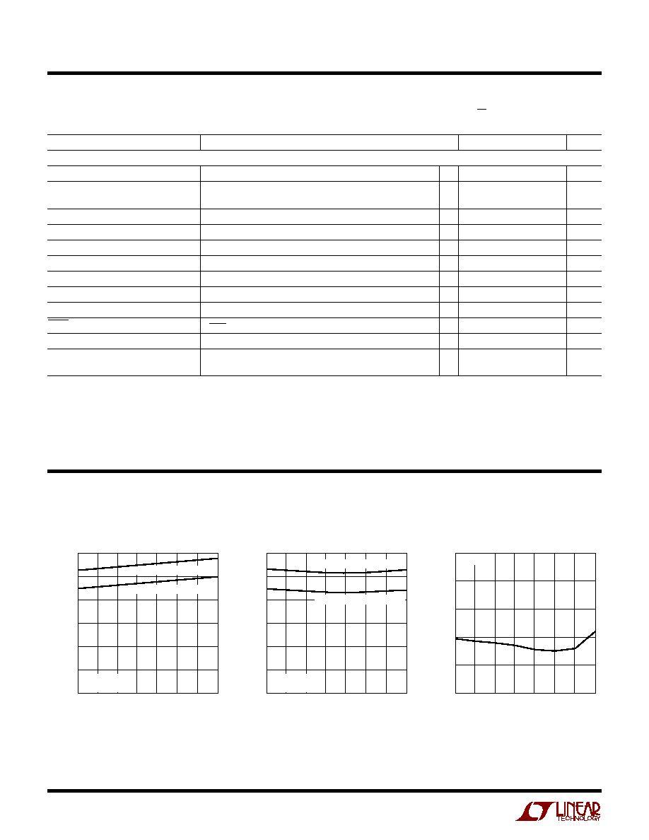
TYPICAL PERFOR A CE CHARACTERISTICS
U
W
Burst Mode Quiescent Current
PWM Mode Quiescent Current
Shutdown Quiescent Current
TEMPERATURE (
∞
C)
≠50
QUIESCENT CURRENT (
µ
A)
120
100
80
60
40
20
0
25
75
3455 G01
≠25
0
50
100
125
V
BAT
= 3.6V
NOT SWITCHING
BOTH SWITCHERS ENABLED
ONLY SWITCHER 1 ENABLED
TEMPERATURE (
∞
C)
≠50
QUIESCENT CURRENT (
µ
A)
600
500
400
300
200
100
0
25
75
3455 G02
≠25
0
50
100
125
BOTH SWITCHERS ENABLED
ONLY SWITCHER 1 ENABLED
V
BAT
= 3.6V
NOT SWITCHING
TEMPERATURE (
∞
C)
≠50
QUIESCENT CURRENT (
µ
A)
5
4
3
2
1
0
25
75
3455 G03
≠25
0
50
100
125
V
BAT
= 3.6V
LTC3455
5
3455f
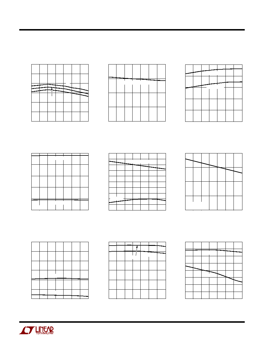
TYPICAL PERFOR A CE CHARACTERISTICS
U
W
Feedback Pins (FB1, FB2)
and AI Pin Voltage
Switching Regulator Oscillator
Frequency
Switching Regulator Current Limit
USB Pin Current Limit
V
MAX
Pin Current Limit
HSO Pin Current Limit
Battery Undervoltage Lockout
USB Undervoltage Lockout
WALLFB Trip Voltage
TEMPERATURE (
∞
C)
≠50
USB PIN CURRENT (mA)
500
400
300
200
100
0
25
75
3455 G07
≠25
0
50
100
125
USBHP = 2V
USBHP = 0V
V
USB
= 5V
TEMPERATURE (
∞
C)
≠50
HSO PIN CURRENT LIMIT (mA)
200
150
100
50
0
25
75
3455 G09
≠25
0
50
100
125
V
HSI
= 3.3V
V
HSO
= 2.5V
TEMPERATURE (
∞
C)
≠50
SWITCHING FREQUENCY (MHz)
2.0
1.5
1.0
0.5
0
25
75
3455 G05
≠25
0
50
100
125
FOR BOTH SWITCHERS
TEMPERATURE (
∞
C)
≠50
CURRENT LIMIT (mA)
1000
800
600
400
200
0
25
75
3455 G06
≠25
0
50
100
125
SWITCHER 1
SWITCHER 2
TEMPERATURE (
∞
C)
≠50
VOLTAGE (mV)
815
810
805
800
795
790
785
25
75
3455 G04
≠25
0
50
100
125
FB1
AI
FB2
TEMPERATURE (
∞
C)
≠50
V
MAX
CURRENT LIMIT (A)
5.0
0.5
1.0
1.5
2.0
2.5
3.0
3.5
4.0
4.5
0
25
75
3455 G08
≠25
0
50
100
125
STARTUP
NORMAL OPERATION
TEMPERATURE (
∞
C)
≠50
BATTERY UVLO (V)
4.00
3.75
3.50
3.25
3.00
2.75
2.50
25
75
3455 G10
≠25
0
50
100
125
FALLING
RISING
TEMPERATURE (
∞
C)
≠50
USB UVLO (V)
4.00
3.75
3.50
3.25
3.00
2.75
2.50
25
75
3455 G11
≠25
0
50
100
125
FALLING
RISING
TEMPERATURE (
∞
C)
≠50
WALLFB TRIP VOLTAGE (V)
1.26
1.24
1.22
1.20
1.18
1.16
1.14
1.12
1.10
25
75
3455 G12
≠25
0
50
100
125
FALLING
RISING