3532f.indd
LTC3532
1
3532f
Micropower Synchronous
Buck-Boost DC/DC Converter
The LTC
®
3532 is a high effi ciency, fi xed frequency, buck-
boost DC/DC converter that operates from input voltages
above, below or equal to the output voltage. The topology
incorporated in the IC provides a continuous transfer
function through all operating modes, making the product
ideal for single lithium-ion, multicell alkaline or NiMH ap-
plications where the output voltage is within the battery
voltage range.
The device includes two 0.36
N-channel MOSFET
switches and two 0.42
P-channel switches. Switching
frequencies up to 2MHz are programmed with an external
resistor. Quiescent current is only 35
A in Burst Mode
operation, maximizing battery life in portable applica-
tions. Automatic Burst Mode operation allows the user
to program the load current for Burst Mode operation or
to control it manually.
Other features include a 1
A shutdown, soft-start control,
thermal shutdown, and peak current limit. The LTC3532 is
available in a low profi le (0.75mm) 10-lead (3mm
× 3mm)
DFN and 10-lead MSOP packages.
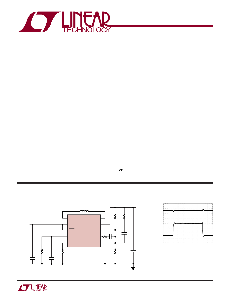
Miniature Hard Disk Drive Power Supply
MP3 Players
Handheld Instruments
Digital Cameras
Handheld Terminals
Single Inductor
Regulated Output with Input Voltages Above, Below
or Equal to the Output
Wide V
IN
Range: 2.4V to 5.5V
V
OUT
Range: 2.4V to 5.25V
Up to 500mA Peak Output Current
Synchronous Rectifi cation: Up to 95% Effi ciency
Manual or Programmable Automatic Burst Mode
®
Operation
Output Disconnect in Shutdown
Programmable Oscillator: 300kHz to 2MHz
Pin Compatible with LTC3440
Small Thermally Enhanced 10-Lead (3mm
× 3mm)
DFN and 10-Lead MSOP Packages
Miniature Hard Disk Drive Power Supply
APPLICATIO S
U
FEATURES
DESCRIPTIO
U
TYPICAL APPLICATIO
U
, LTC and LT are registered trademarks of Linear Technology Corporation.
BurstMode is a registered trademark of Linear Technology Corporation.
All other trademarks are the property of their respective owners.
SW1
V
IN
SHDN/SS
BURST
R
T
SW2
V
OUT
FB
V
C
GND
LTC3532
3532 TA01
43.2k
0.01
µF
200k
4.7
µF
V
IN
Li-Ion
2.5V TO 4.2V
4.7
µH
V
OUT
3.3V
100mA
TO 500mA
(PEAK)
10
µF
33pF
1k
340k
12.1k
220pF
200k
V
OUT
200mV/DIV
I
LOAD
100mA/DIV
100
µs/DIV
V
IN
= 3V
V
OUT
= 3.3V
I
LOAD
= 50mA TO 300mA
3532 TA01b
LTC3532
2
3532f
BURST, V
IN
, V
OUT
, V
C
, FB
..................................
0.3V to 6V
R
T
..................................................................... 0V to 5V
S
H
D
N/SS ..................................................... 0.3V to 6V
SW1, SW2
DC ............................................................ 0.3V to 6V
Pulsed < 100ns ........................................ 0.3V to 7V
(Note 1)
The
denotes the specifi cations which apply over the full operating
temperature range, otherwise specifi cations are at T
A
= 25°C. V
IN
= V
OUT
= 3.6V, R
T
= 64.9k, unless otherwise specifi ed.
PARAMETER
CONDITIONS
MIN
TYP
MAX
UNITS
Input Start-Up Voltage
2.3
2.4
V
Input Operating Range
2.4
5.5
V
Output Voltage Adjust Range
2.4
5.25
V
Feedback Voltage
1.19
1.22
1.25
V
Feedback Input Current
V
FB
= 1.22V
1
50
nA
Quiescent Current, Burst Mode Operation
BURST = 0V
35
60
µA
Quiescent Current, Shutdown
S
H
D
N = 0V, Not Including Switch Leakage, V
OUT
= 0V
0.1
1
µA
Quiescent Current, Active
V
C
= 0V, MODE/SYNC = 0V, BURST = V
IN
(Note 3)
600
1000
µA
NMOS Switch Leakage
Switches B and C
0.1
5
µA
PMOS Switch Leakage
Switches A and D
0.1
10
µA
NMOS Switch On Resistance
Switches B and C
0.36
PMOS Switch On Resistance
Switches A and D
0.42
Input Current Limit
0.8
1.1
1.45
A
ELECTRICAL CHARACTERISTICS
ABSOLUTE AXI U
RATI GS
W
W
W
U
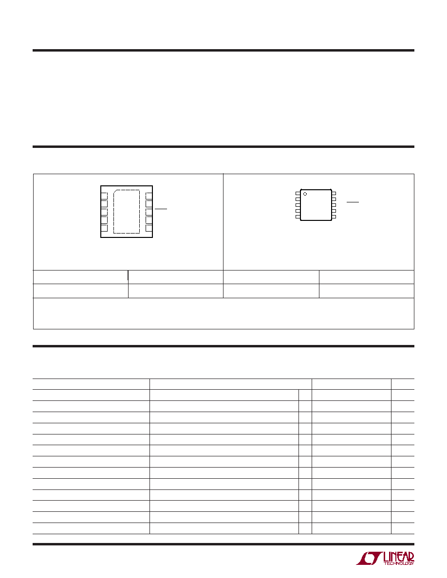
ORDER PART NUMBER
DD PART MARKING
Consult LTC Marketing for parts specifi ed with wider operating temperature ranges.
LBXR
LTC3532EDD
PACKAGE/ORDER I FOR ATIO
U
U
W
T
JMAX
= 125°C,
JA
= 43°C/W
EXPOSED PAD (PIN 11) IS GND, MUST BE CONNECTED TO PCB
ORDER PART NUMBER
MS PART MARKING
LTBXS
LTC3532EMS
Order Options Tape and Reel: Add #TR
Lead Free: Add #PBF Lead Free Tape and Reel: Add #TRPBF
Lead Free Part Marking:
http://www.linear.com/leadfree/
T
JMAX
= 125°C
JA
= 130°C/W 1 LAYER BOARD
JA
= 100°C/W 4 LAYER BOARD
JC
= 45°C/W
Operating Temperature Range (Note 2) ... 40°C to 85°C
Storage Temperature Range
DD ..................................................... 65°C to 125°C
MSOP ................................................ 65°C to 150°C
Lead Temperature (Soldering,10 sec)
MSOP
............................................................... 300°C
TOP VIEW
DD PACKAGE
10-LEAD (3mm
× 3mm) PLASTIC DFN
10
9
6
7
8
4
5
3
2
1
V
C
FB
SHDN/SS
V
IN
V
OUT
R
T
BURST
SW1
SW2
GND
11
1
2
3
4
5
R
T
BURST
SW1
SW2
GND
10
9
8
7
6
V
C
FB
SHDN/SS
V
IN
V
OUT
TOP VIEW
MS PACKAGE
10-LEAD PLASTIC MSOP
LTC3532
3
3532f
The
denotes the specifi cations which apply over the full operating
temperature range, otherwise specifi cations are at T
A
= 25°C. V
IN
= V
OUT
= 3.6V, R
T
= 64.9k, unless otherwise specifi ed.
ELECTRICAL CHARACTERISTICS
PARAMETER
CONDITIONS
MIN
TYP
MAX
UNITS
Maximum Duty Cycle
Boost (% Switch C On)
Buck (% Switch A On)
70
100
88
%
%
Minimum Duty Cycle
0
%
Frequency Accuracy
575
740
885
kHz
Burst Threshold (Falling)
0.88
V
Burst Threshold (Rising)
1.12
V
Burst Current Ratio
Ratio of I
OUT
to I
BURST
8000
Error Amp AVOL
90
dB
Error Amp Source Current
V
C
= 1.4V
15
µA
Error Amp Sink Current
V
C
= 2V
310
µA
SHDN/SS Threshold
When IC is Enabled
When EA is at Maximum Boost Duty Cycle
0.4
1
2.2
1.5
V
V
SHDN/SS Input Current
V
SHDN
= 5.5V
0.01
1
µA
Note 1: Stresses beyond those listed under Absolute Maximum Ratings
may cause permanent damage to the device. Exposure to any Absolute
Maximum Rating condition for extended periods may affect device
reliability and lifetime.
Note 2: The LTC3532E is guaranteed to meet performance specifications
from 0°C to 70°C. Specifications over the 40°C to 85°C operating
temperature range are assured by design, characterization and correlations
with statistical process controls.
Note 3: Current measurements are performed when the outputs are not
switching.
Note 4: This IC includes overtemperature protection that is intended
to protect the device during momentary overload conditions. Junction
temperature will exceed 125°C when overtemperature protection is active.
Continuous operation above the specified maximum operating junction
temperature may result in device degradation or failure.
Effi ciency and Power Loss
vs Load Autoburst Mode
Effi ciency and Power Loss
vs Load
Fixed Frequency and Burst Mode
Quiescent Current vs V
IN
TYPICAL PERFOR A CE CHARACTERISTICS
U
W
T
A
= 25°C, unless otherwise specifi ed.
LOAD CURRENT (mA)
60
EFFICIENCY (%)
POWER LOSS (mW)
80
100
50
70
90
0.1
10
100
1000
3532 G01
40
1
10
1000
0.1
100
0.01
1
POWER LOSS
V
OUT
= 3.3V
EFFICIENCY
3V
3.6V
4.2V
LOAD CURRENT (mA)
60
EFFICIENCY (%)
POWER LOSS (mW)
80
100
50
70
90
0.1
10
100
1000
3532 G02
40
1
1000
100
10
1
0.1
BURST EFFICIENCY
FIXED FREQUENCY
EFFICIENCY
FIXED FREQUENCY
POWER LOSS
BURST
POWER LOSS
V
IN
(V)
2.5
0
V
IN
QUIESCENT CURRENT (mA)
0.5
1.0
1.5
2.0
2.5
3.0
3.5
4.5
5.5
3532 G03
V
IN
QUIESCENT CURRENT BURST MODE (
µ
A)
75
80
70
65
55
50
45
60
40
BURST MODE
2000kHz
1000kHz
500kHz
1500kHz
NOT SWITCHING
LTC3532
4
3532f
TEMPERATURE (
°C)
V
IN
= 3.6V
55
FREQUENCY (MHz)
1000
1050
1100
95
3532 G07
950
900
800
5
45
850
1200
1150
TEMPERATURE (
°C)
55
1.196
FEEDBACK VOLTAGE (V)
1.201
1.211
1.216
1.221
45
1.241
3532 G08
1.206
5
95
1.226
1.231
1.236
V
OUT
200mV/DIV
I
LOAD
100mA/DIV
100
µs/DIV
C
OUT
= 10
µF
V
IN
= 3.6V
V
OUT
= 3.3V
3535 G09
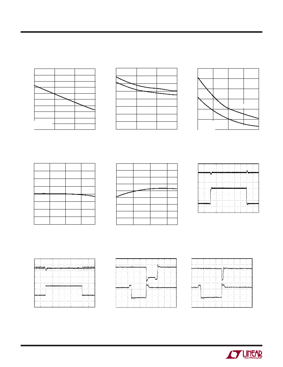
Effi ciency vs Frequency
Peak Current Clamp and Limit
vs V
IN
Automatic Burst Threshold
vs R
BURST
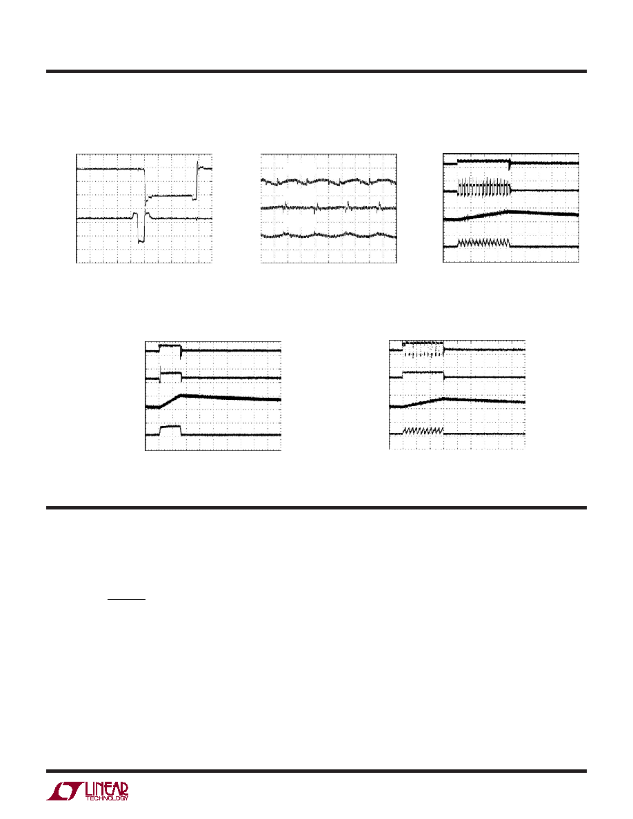
Burst Mode to Fixed Frequency
Transition
Switch Pins in Buck-Boost Mode
Switch Pins Before Entering
Boost Mode
TYPICAL PERFOR A CE CHARACTERISTICS
U
W
Frequency vs Temperature
Feedback Voltage vs Temperature
Load Transient Response in
Fixed Frequency Mode
T
A
= 25°C, unless otherwise specifi ed.
FREQUENCY (kHz)
500
80
EFFICIENCY (%)
84
86
88
90
92
94
1000
1500
3532 G04
96
98
100
82
2000
V
IN
= 3.6V
V
OUT
= 3.3V
V
IN
(V)
2.4
INPUT CURRENT (A)
0.8
1.0
1.2
5.4
3532 G05
0.6
0.4
0
3.4
4.4
0.2
1.6
1.4
V
OUT
= 3.3V
I
CLAMP
I
LIMIT
BURST RESISTOR (k
)
150
10
LOAD CURRENT (mA)
20
30
40
50
60
70
250
350
450
550
3532 G06
LEAVE BURST
ENTER BURST
V
OUT
= 3.3V
V
IN
= 3.6V
SW1
2V/DIV
SW2
2V/DIV
40ns/DIV
V
IN
= 3.3V
V
OUT
= 3.3V
I
LOAD
= 100mA
3532 G11
SW1
2V/DIV
SW2
2V/DIV
40ns/DIV
V
IN
= 2.9V
V
OUT
= 3.3V
I
LOAD
= 100mA
3532 G12
V
OUT
200mV/DIV
BURST PIN
2V/DIV
400
µs/DIV
C
OUT
= 22
µF
V
IN
= 3.6V
V
OUT
= 3.3V
3532 G10
LTC3532
5
3532f
SW2
5V/DIV
SW1
5V/DIV
INDUCTOR
CURRENT
500mA/DIV
V
OUT
100mV/DIV
4
µs/DIV
V
IN
= 4.2V
V
OUT
= 3.3V
I
LOAD
= 20mA
C
OUT
= 22
µF
3535 G17
SW2
5V/DIV
SW1
5V/DIV
INDUCTOR
CURRENT
500mA/DIV
V
OUT
100mV/DIV
4
µs/DIV
V
IN
= 3.75V
V
OUT
= 3.3V
I
LOAD
= 20mA
C
OUT
= 22
µF
340612 G16
PI FU CTIO S
U
U
U
RT (Pin 1): Timing Resistor to Program the Oscillator
Frequency. The programming range is 300kHz to 2MHz.
f kHz
R k
T
(
)
,
(
)
=
48 000
BURST (Pin 2): Used to Set the Automatic Burst Mode Op-
eration Threshold. Place a resistor and capacitor in parallel
from this pin to ground. See the Applications Information
section for component value selection. For manual control,
ground the pin to force Burst Mode operation, connect to
V
OUT
to force fi xed frequency mode.
SW1 (Pin 3): Switch Pin Where the Internal Switches A
and B are Connected. Connect inductor from SW1 to SW2.
An optional Schottky diode can be connected from SW1
to ground. Minimize trace length to minimize EMI.
SW2 (Pin 4): Switch Pin Where the Internal Switches C
and D are Connected. For applications with output voltages
over 4.3V, a Schottky diode is required from SW2 to V
OUT
to ensure SW2 does not exhibit excess voltage.
GND (Pin 5): Signal and Power Ground for the IC.
V
OUT
(Pin 6): Output of the Synchronous Rectifi er. A fi lter
capacitor is placed from V
OUT
to GND.
V
IN
(Pin 7): Input Supply Pin. Supplies current to the
inductor through SW1 and supplies internal V
CC
for the
IC. A ceramic bypass capacitor as close to the V
IN
pin and
GND (Pin 5) is required.
Switch Pins Before Entering
Buck Mode
Output Ripple at 100mA Load
Burst Mode, Boost
TYPICAL PERFOR A CE CHARACTERISTICS
U
W
T
A
= 25°C, unless otherwise specifi ed.
Burst Mode, Buck-Boost
Burst Mode, Buck
SW1
2VDIV
SW2
2VDIV
40ns/DIV
V
IN
= 4V
VOUT = 3.3V
I
LOAD
= 100mA
3535 G13
V
OUT
50mV/DIV
V
OUT
50mV/DIV
V
OUT
50mV/DIV
400ns/DIV
V
OUT
= 3.6V
I
OUT
= 100mA
C
OUT
= 10
µF
3535 G14
V
IN
= 2.4V
V
IN
= 3.6V
V
IN
= 4.5V
SW1
5V/DIV
SW2
5V/DIV
INDUCTOR
CURRENT
500mA/DIV
V
OUT
100mV/DIV
4
µs/DIV
V
IN
= 2.4V
V
OUT
= 3.3V
I
LOAD
= 20mA
C
OUT
= 22
µF
3535 G15