 | ÐлекÑÑоннÑй компоненÑ: LTC3703EG | СкаÑаÑÑ:  PDF PDF  ZIP ZIP |
Äîêóìåíòàöèÿ è îïèñàíèÿ www.docs.chipfind.ru
LTC3703
1
3703f
APPLICATIO S
U
DESCRIPTIO
U
FEATURES
TYPICAL APPLICATIO
U
, LTC and LT are registered trademarks of Linear Technology Corporation.
s
High Voltage Operation: Up to 100V
s
Large 1
Gate Drivers
s
No Current Sense Resistor Required
s
Step-Up or Step-Down DC/DC Converter
s
Dual N-Channel MOSFET Synchronous Drive
s
Excellent Transient Response and DC Line Regulation
s
Programmable Constant Frequency: 100kHz to
600kHz
s
±
1% Reference Accuracy
s
Synchronizable up to 600kHz
s
Selectable Pulse Skip Mode Operation
s
Low Shutdown Current: 50
µ
A Typ
s
Programmable Current Limit
s
Undervoltage Lockout
s
Programmable Soft-Start
s
16-Pin Narrow SSOP and 28-Pin SSOP Packages
The LTC
®
3703 is a synchronous step-down switching
regulator controller that can directly step-down voltages
from up to 100V, making it ideal for telecom and automo-
tive applications. The LTC3703 drives external N-channel
MOSFETs using a constant frequency (up to 600kHz),
voltage mode architecture. The external component count
has been minimized, providing a compact overall solution
footprint.
A precise internal reference provides 1% DC accuracy. A
high bandwidth error amplifier and patented line feed
forward compensation provide very fast line and load
transient response. Strong 1
gate drivers allow the
LTC3703 to drive multiple MOSFETs for higher current
applications. The operating frequency is user program-
mable from 100kHz to 600kHz and can also be synchro-
nized to an external clock for noise-sensitive applications.
Current limit is programmable with an external resistor
and utilizes the voltage drop across the synchronous
MOSFET to eliminate the need for a current sense resistor.
Soft- start is provided by an external capacitor. Pulling the
soft-start pin low shuts down the LTC3703, reducing
supply current to 50
µ
A.
s
48V Telecom and Base Station Power Supplies
s
Networking Equipment, Servers
s
Automotive and Industrial Control
100V Synchronous
Switching Regulator
Controller
Efficiency vs Load Current
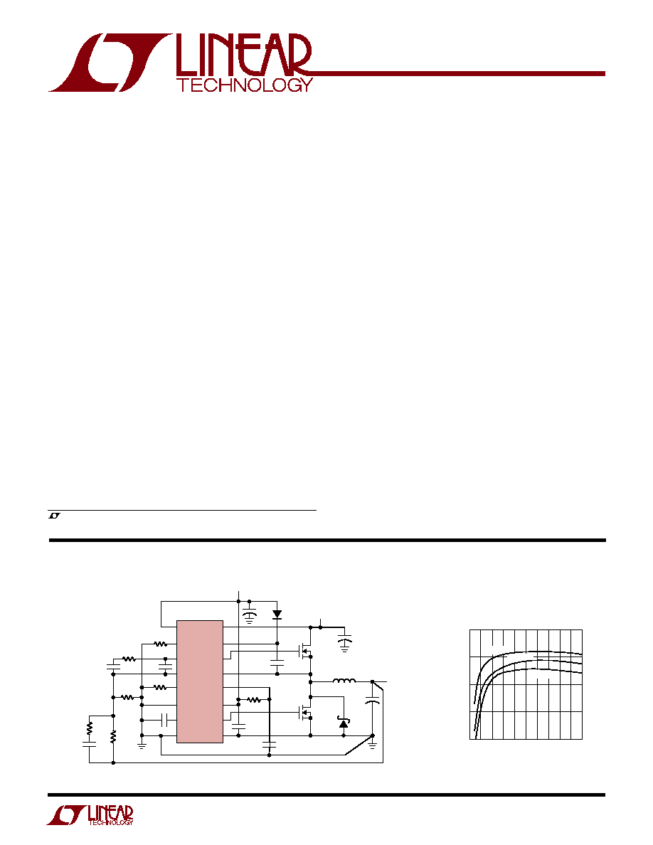
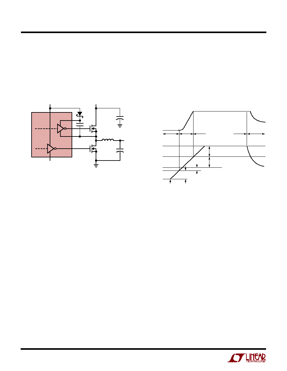
Figure 1. High Efficiency High Voltage Step-Down Converter
LTC3703
MODE/SYNC
FSET
COMP
FB
I
MAX
INV
RUN/SS
GND
V
IN
BOOST
TG
SW
VCC
DRV
CC
BG
BGRTN
22
µ
F
×
2
3300pF
1500pF
22k
330
113k
1%
8.06k
1%
10
15k
30k
0.1
µ
F
V
IN
15V TO 100V
Si7456DP
8
µ
H
MBR1100
V
OUT
12V
5A
220
µ
F
25V
×
2
BAS21
V
CC
9.3V TO 15V
0.1
µ
F
3703 F01
10
µ
F
1
µ
F
+
+
+
Si7456DP
22
µ
F
25V
15pF
LOAD (A)
0
EFFICIENCY (
%
)
100
95
90
85
80
4
3703 F01b
1
2
3
5
V
IN
= 25V
V
IN
= 50V
V
IN
= 75V
LTC3703
2
3703f
Supply Voltages
V
CC
, DRV
CC
.......................................... 0.3V to 15V
(DRV
CC
BGRTN), (BOOST SW) ...... 0.3V to 15V
BOOST ................................................ 0.3V to 115V
BGRTN ...................................................... 5V to 0V
V
IN
Voltage ............................................. 0.3V to 100V
SW Voltage ................................................ 1V to 100V
Run/SS Voltage .......................................... 0.3V to 5V
ABSOLUTE AXI U
RATI GS
W
W
W
U
(Note 1)
ELECTRICAL CHARACTERISTICS
The
q
denotes the specifications which apply over the full operating
temperature range, otherwise specifications are at T
A
= 25
°
C. V
CC
= DRV
CC
= V
BOOST
= V
IN
= 10V, V
MODE/SYNC
= V
INV
= V
SW
=
BGRTN = 0V, RUN/SS = I
MAX
= open, R
SET
= 25k, unless otherwise specified.
SYMBOL
PARAMETER
CONDITIONS
MIN
TYP
MAX
UNITS
V
CC
, DRV
CC
V
CC
, DRV
CC
Supply Voltage
q
9.3
15
V
V
IN
V
IN
Pin Voltage
q
100
V
I
CC
V
CC
Supply Current
V
FB
= 0V
q
1.7
2.5
mA
RUN/SS = 0V
50
µ
A
I
DRVCC
DRV
CC
Supply Current
(Note 5)
0
5
µ
A
RUN/SS = 0V
0
5
µ
A
I
BOOST
BOOST Supply Current
(Note 5)
q
360
500
µ
A
RUN/SS = 0V
0
5
µ
A
MODE/SYNC, INV Voltages ....................... 0.3V to 15V
f
SET
, FB, I
MAX
Voltages ............................... 0.3V to 3V
Peak Output Current <10
µ
s BG,TG ............................ 5A
Operating Temperature Range (Note 2) .. 40
°
C to 85
°
C
Junction Temperature (Notes 3, 7) ....................... 125
°
C
Storage Temperature Range ................. 65
°
C to 150
°
C
Lead Temperature (Soldering, 10 sec.)................. 300
°
C
ORDER PART
NUMBER
GN PART
MARKING
T
JMAX
= 125
°
C,
JA
= 110
°
C/W
3703
LTC3703EGN
PACKAGE/ORDER I FOR ATIO
U
U
W
Consult LTC Marketing for parts specified with wider operating temperature ranges.
ORDER PART
NUMBER
LTC3703EG
1
2
3
4
5
6
7
8
9
10
11
12
13
14
TOP VIEW
G PACKAGE
28-LEAD PLASTIC SSOP
28
27
26
25
24
23
22
21
20
19
18
17
16
15
BOOST
TG
SW
NC
NC
NC
NC
V
CC
DRV
CC
BG
NC
NC
NC
BGRTN
V
IN
NC
NC
NC
NC
MODE/SYNC
f
SET
COMP
FB
I
MAX
INV
NC
RUN/SS
GND
TOP VIEW
GN PACKAGE
16-LEAD NARROW PLASTIC SSOP
1
2
3
4
5
6
7
8
16
15
14
13
12
11
10
9
MODE/SYNC
f
SET
COMP
FB
I
MAX
INV
RUN/SS
GND
V
IN
B00ST
TG
SW
V
CC
DRV
CC
BG
BGRTN
T
JMAX
= 125
°
C,
JA
= 100
°
C/W
LTC3703
3
3703f
Note 1: Absolute Maximum Ratings are those values beyond which the life of
a device may be impaired.
Note 2: The LTC3703E is guaranteed to meet performance specifications
from 0
°
C to 70
°
C. Specifications over the 40
°
C to 85
°
C operating
temperature range are assured by design, characterization and correlation
with statistical process controls.
Note 3: T
J
is calculated from the ambient temperature T
A
and power
dissipation P
D
according to the following formula:
LTC3703: T
J
= T
A
+ (P
D
· 100
°
C/W) G Package
Note 4: The LTC3703 is tested in a feedback loop that servos V
FB
to the
reference voltage with the COMP pin forced to a voltage between 1V and 2V.
ELECTRICAL CHARACTERISTICS
The
q
denotes the specifications which apply over the full operating
temperature range, otherwise specifications are at T
A
= 25
°
C. V
CC
= DRV
CC
= V
BOOST
= V
IN
= 10V, V
MODE/SYNC
= V
INV
= V
SW
=
BGRTN = 0V, RUN/SS = I
MAX
= open, R
SET
= 25k, unless otherwise specified.
Note 5: The dynamic input supply current is higher due to the power
MOSFET gate charging being delivered at the switching frequency
(Q
G
· f
OSC
).
Note 6: Guaranteed by design. Not subject to test.
Note 7: This IC includes overtemperature protection that is intended to
protect the device during momentary overload conditions. Junction
temperature will exceed 125
°
C when overtemperature protection is active.
Continuous operation above the specified maximum operating junction
temperature may impair device reliability.
Note 8: R
DS(ON)
guaranteed by correlation to wafer level measurement.
SYMBOL
PARAMETER
CONDITIONS
MIN
TYP
MAX
UNITS
Main Control Loop
V
FB
Feedback Voltage
(Note 4)
0.792
0.800
0.808
V
q
0.788
0.812
V
V
FB, LINE
Feedback Voltage Line Regulation
9V < V
CC
< 15V (Note 4)
q
0.007
0.05
%/V
V
FB, LOAD
Feedback Voltage Load Regulation
1V < V
COMP
< 2V (Note 4)
q
0.01
0.1
%
V
MODE/SYNC
MODE/SYNC Threshold
MODE/SYNC Rising
0.75
0.8
0.87
V
V
MODE/SYNC
MODE/SYNC Hysteresis
20
mV
I
MODE/SYNC
MODE/SYNC Current
0
V
MODE/SYNC
15V
0
1
µ
A
V
INV
Invert Threshold
1
1.5
2
V
I
INV
Invert Current
0
V
INV
15V
0
1
µ
A
I
VIN
V
IN
Sense Input Current
V
IN
= 100V
100
140
µ
A
RUN/SS = 0V, V
IN
= 10V
0
1
µ
A
I
MAX
I
MAX
Source Current
V
IMAX
= 0V
10.5
12
13.5
µ
A
V
OS,
IMAX
V
IMAX
Offset Voltage
|V
SW
| V
IMAX
at I
RUN/SS
= 0
µ
A
25
10
55
mV
V
RUN/SS
Shutdown Threshold
0.7
0.9
1.2
V
I
RUN/SS
RUN/SS Source Current
RUN/SS = 0V
2.5
4
5.5
µ
A
Maximum RUN/SS Sink Current
|V
SW
| V
IMAX
> 100mV
9
17
25
µ
A
V
UV
Undervoltage Lockout
V
CC
Rising
q
8.0
8.7
9.3
V
V
CC
Falling
q
5.7
6.2
6.8
V
Oscillator
f
OSC
Oscillator Frequency
R
SET
= 25k
270
300
330
kHz
f
SYNC
External Sync Frequency Range
100
600
kHz
t
ON, MIN
Minimum On-Time
200
ns
DC
MAX
Maximum Duty Cycle
f < 200kHz
89
93
96
%
Driver
I
BG, PEAK
BG Driver Peak Source Current
1.5
2
A
R
BG, SINK
BG Driver Pull-Down R
DS, ON
(Note 8)
1
1.5
I
TG, PEAK
TG Driver Peak Source Current
1.5
2
A
R
TG, SINK
TG Driver Pull-Down R
DS, ON
(Note 8)
1
1.5
Feedback Amplifier
A
VOL
Op Amp DC Open Loop Gain
(Note 4)
74
85
dB
f
U
Op Amp Unity Gain Crossover Frequency (Note 6)
25
MHz
I
FB
FB Input Current
0
V
FB
3V
0
1
µ
A
I
COMP
COMP Sink/Source Current
±
5
±
10
mA
LTC3703
4
3703f
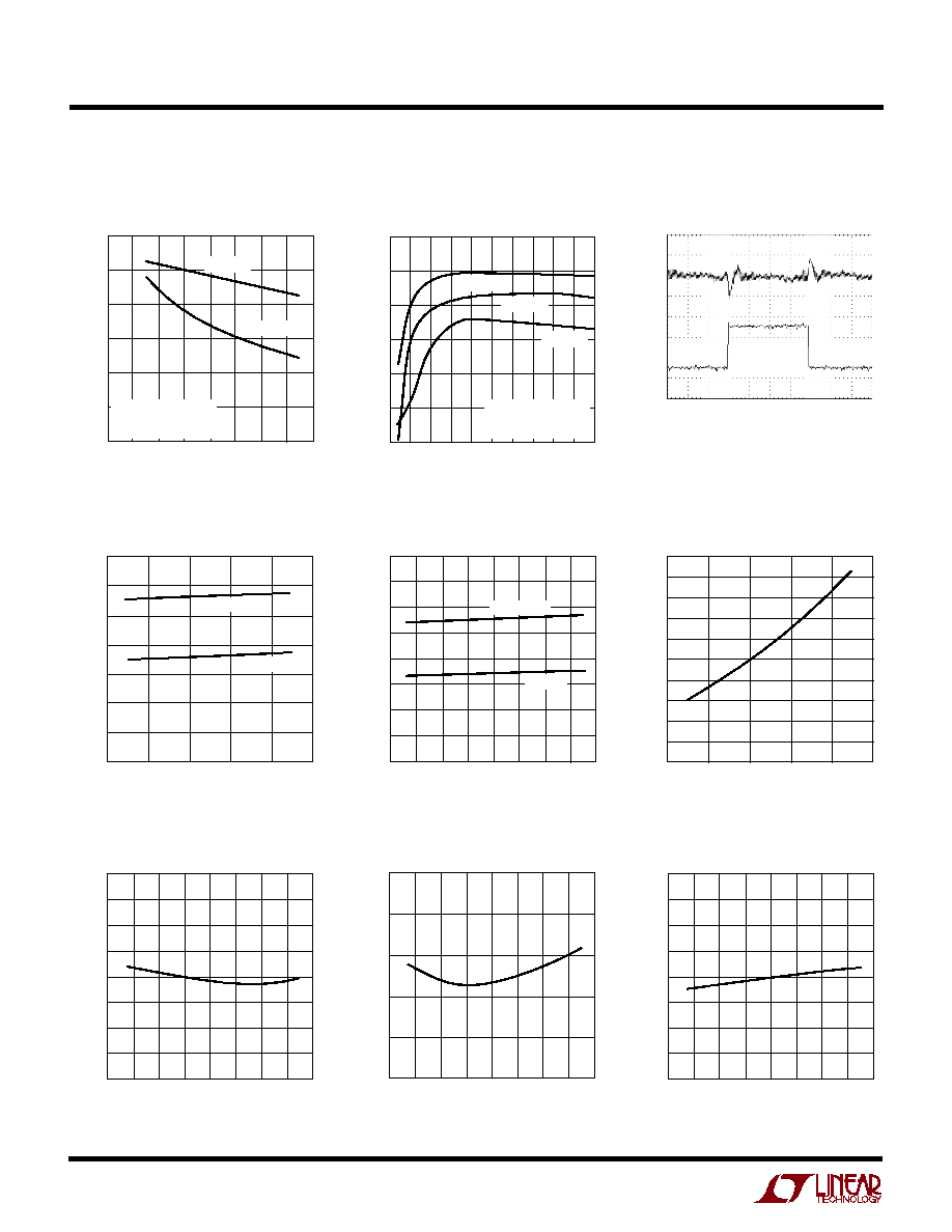
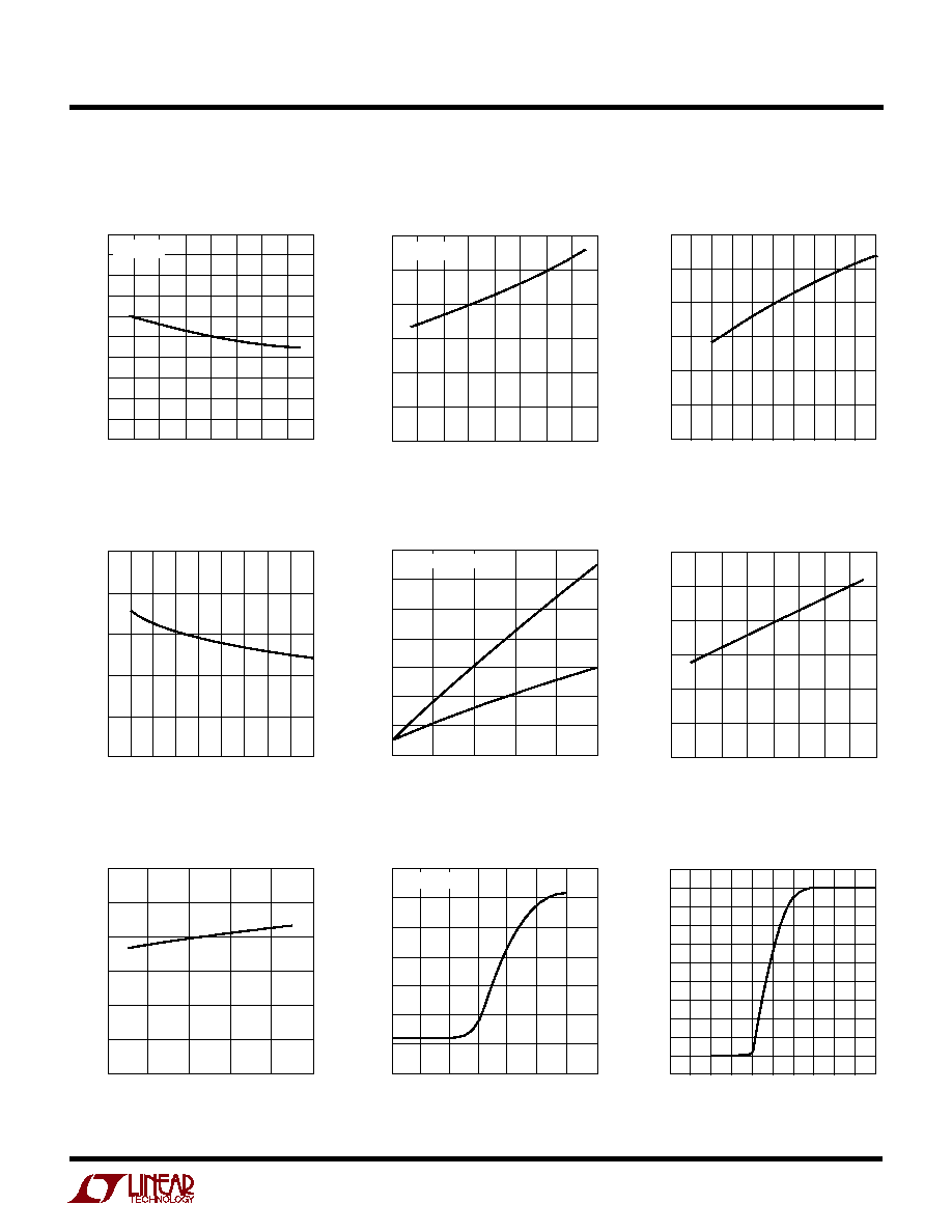
TYPICAL PERFOR A CE CHARACTERISTICS
U
W
Efficiency vs Input Voltage
Efficiency vs Load Current
Load Transient Response
V
CC
Current vs V
CC
Voltage
V
CC
Current vs Temperature
V
CC
Shut-Down Current vs V
CC
Voltage
V
CC
Shut-Down Current vs
Temperature
Reference Voltage vs
Temperature
Normalized Frequency vs
Temperature
TEMPERATURE (
°
C)
60 40 20
0
60
100
20
40
80
TEMPERATURE (
°
C)
60 40 20
0
60
100
20
40
80
60 40 20
0
20
40
60
80
100
TEMPERATURE (
°
C)
NORMALIZED FREQUENCY
3703 G09
1.20
1.15
1.10
1.05
1.00
0.95
0.90
0.85
0.80
INPUT VOLTAGE (V)
EFFICIENCY (%)
3703 G01
100
95
90
85
80
75
70
0
20
40
50
10
30
60
70
80
LOAD CURRENT (A)
0
0.5
1.5
2.5
3.5
4.5
EFFICIENCY (%)
100
95
90
85
80
75
70
1.0
2.0
3.0
4.0
3703 G02
5.0
V
CC
VOLTAGE (V)
6
3.5
3.0
2.5
2.0
1.5
1.0
0.5
0
12
3703 G04
8
10
14
16
V
CC
CURRENT (mA)
TEMPERATURE (
°
C)
60 40 20
0
V
CC
CURRENT (mA)
60
100
3703 G05
20
40
80
4
3
2
1
0
3703 G03
V
CC
VOLTAGE (V)
6
V
CC
CURRENT (
µ
A)
100
90
80
70
60
50
40
30
20
10
0
14
3703 G06
8
10
12
16
V
CC
CURRENT (
µ
A)
3703 G07
70
65
60
55
50
45
40
35
30
REFERENCE VOLTAGE (V)
0.803
0.802
0.801
0.800
0.799
0.798
3703 G08
V
OUT
= 12V
f = 300kHz
PULSE SKIP DISABLED
V
OUT
= 5V
f = 250kHz
PULSE SKIP ENABLED
I
OUT
= 0.5A
I
OUT
= 5A
V
IN
= 75V
V
IN
= 45V
V
IN
= 15V
V
OUT
50mV/DIV
I
OUT
2A/DIV
V
IN
= 50V
V
OUT
= 12V
1A TO 5A LOAD STEP
50
µ
s/DIV
V
FB
= 0V
COMP = 1.5V
V
FB
= 0V
COMP = 1.5V
T
A
= 25
°
C (unless otherwise noted).
LTC3703
5
3703f
PEAK SOURCE CURRENT (A)
3.0
2.8
2.6
2.4
2.2
2.0
1.8
1.6
1.4
1.2
1.0
3703 G10
TEMPERATURE (
°
C)
R
DS(ON)
(
)
3703 G11
1.2
1.0
0.8
0.6
0.4
0.2
0
DRV
CC
/BOOST VOLTAGE (V)
5
6
8
10
12
14
PEAK SOURCE CURRENT (A)
3.0
2.5
2.0
1.5
1.0
0.5
0
7
9
11
13
3703 G12
15
DRV
CC
/BOOST VOLTAGE (V)
6
R
DS(ON)
(
)
0.6
0.8
0.9
1.0
1.1
8
10
11
15
3703 G13
0.7
7
9
12
13
14
60 40 20
0
20
40
60
80
100
60 40 20
0
20
40
60
80
100
TEMPERATURE (
°
C)
V
CC
= 10V
V
CC
= 10V
|SW| VOLTAGE (V)
0
25
20
15
10
5
0
5
10
0.3
0.5
3703 G17
0.1
0.2
0.4
0.6
0.7
RUN/SS SINK CURRENT (
µ
A)
RUN VOLTAGE (V)
0.5
MAX DUTY CYCLE (%)
100
90
80
70
60
50
40
30
20
10
0
10
2.5
3703 G18
1.0
1.5
2.0
3.0
I
MAX
= 0.3V
GATE CAPACITANCE (pF)
0
70
60
50
40
30
20
10
0
6000
3703 G14
2000
4000
8000
10000
RISE/FALL TIME (ns)
DRVCC, BOOST = 10V
RISE
FALL
TEMPERATURE (
°
C)
RUN/SS CURRENT (
µ
A)
1573 G06
6
5
4
3
2
1
0
60
20
20
40
40
0
60
80
100
V
CC
VOLTAGE (V)
6
RUN/SS PULLUP CURRENT (
µ
A)
6
5
4
3
2
1
0
8
10
12
14
3703 G16
16
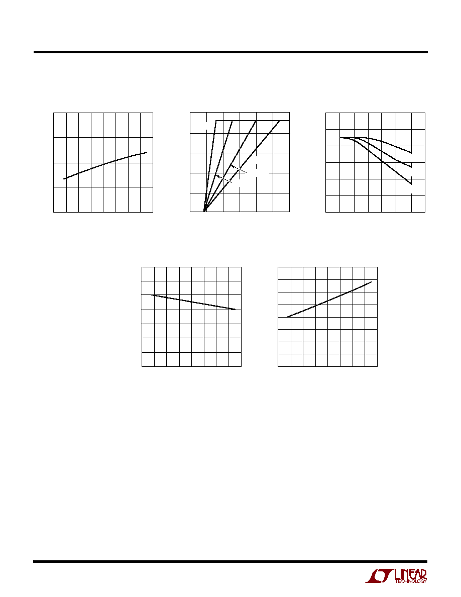
TYPICAL PERFOR A CE CHARACTERISTICS
U
W
Driver Peak Source Current vs
Temperature
Driver Pull-Down R
DS(ON)
vs
Temperature
Driver Peak Source Current vs
Supply Voltage
Rise/Fall Time vs Gate
Capacitance
RUN/SS Pull-Up Current vs
Temperature
RUN/SS Pull-Up Current vs
V
CC
Voltage
RUN/SS Sink Current vs
SW
Voltage
Max % DC vs RUN/SS Voltage
Driver Pull-Down R
DS(ON)
vs
Supply Voltage
LTC3703
6
3703f
TYPICAL PERFOR A CE CHARACTERISTICS
U
W
I
MAX
Current vs Temperature
% Duty Cycle vs COMP Voltage
Max % DC vs Frequency and
Temperature
Shutdown Threshold vs
Temperature
t
ON(MIN)
vs Temperature
I
MAX
SOURCE CURRENT (
µ
A)
13
12
11
3703 G19
FREQUENCY (kHz)
MAX DUTY CYCLE (%)
3703 G21
100
95
90
85
80
75
70
0
200
400
500
100
300
600
700
TEMPERATURE (
°
C)
SHUTDOWN THRESHOLD (V)
1.4
1.2
1.0
0.8
0.6
0.4
0.2
0
3703 G22
3703 G23
t
ON(MIN)
(ns)
160
140
120
100
80
60
40
20
0
60 40 20
0
20
40
60
80
100
TEMPERATURE (
°
C)
60 40 20
0
20
40
60
80
100
60 40 20
0
20
40
60
80
100
TEMPERATURE (
°
C)
25
°
C
45
°
C
90
°
C
COMP (V)
0.5
DUTY CYCLE (%)
100
80
60
40
20
0
0.75
1.00
1.25
1.50
3703 G20
1.75
2.00
V
IN
= 10V
V
IN
= 75V
V
IN
= 50V
V
IN
= 25V

LTC3703
7
3703f
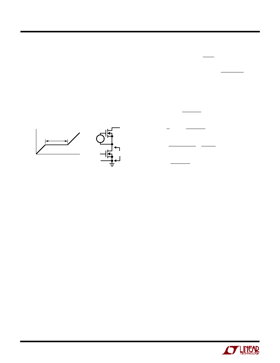
MODE/SYNC
(Pin 1): Pulse Skip Mode Enable/Sync Pin.
This multifunction pin provides Pulse Skip Mode enable/
disable control and an external clock input for synchroni-
zation of the internal oscillator. Pulling this pin below 0.8V
or to an external logic-level synchronization signal dis-
ables Pulse Skip Mode operation and forces continuous
operation. Pulling the pin above 0.8V enables Pulse Skip
Mode operation. This pin can also be connected to a
feedback resistor divider from a secondary winding on the
inductor to regulate a second output voltage.
f
SET
(Pin 2): Frequency Set. A resistor connected to this
pin sets the free running frequency of the internal oscilla-
tor. See applications section for resistor value selection
details.
COMP (Pin 3): Loop Compensation. This pin is connected
directly to the output of the internal error amplifier. An RC
network is used at the COMP pin to compensate the
feedback loop for optimal transient response.
FB (Pin 4): Feedback Input. Connect FB through a resistor
divider network to V
OUT
to set the output voltage. Also
connect the loop compensation network from COMP to
FB.
I
MAX
(Pin 5): Current Limit Set. The I
MAX
pin sets the
current limit comparator threshold. If the voltage drop
across the bottom MOSFET exceeds the magnitude of the
voltage at I
MAX
, the controller goes into current limit. The
I
MAX
pin has an internal 12
µ
A current source, allowing the
current threshold to be set with a single external resistor
to ground. See the Current Limit Programming section for
more information on choosing R
IMAX
.
INV (Pin 6): Top/Bottom Gate Invert. Pulling this pin above
2V sets the controller to operate in step-up (boost) mode
with the TG output driving the synchronous MOSFET and
the BG output driving the main switch. Below 1V, the
controller will operate in step-down (buck) mode.
RUN/SS (Pin 7): Run/Soft-Start. Pulling RUN/SS below
0.9V will shut down the LTC3703, turn off both of the
external MOSFET switches and reduce the quiescent sup-
ply current to 50
µ
A. A capacitor from RUN/SS to ground
will control the turn-on time and rate of rise of the output
voltage at power-up. An internal 4
µ
A current source pull-
up at the RUN/SS pin sets the turn-on time at approxi-
mately 750ms/
µ
F.
GND (Pin 8): Ground Pin.
BGRTN (Pin 9): Bottom Gate Return. This pin connects to
the source of the pull-down MOSFET in the BG driver and
is normally connected to ground. Connecting a negative
supply to this pin allows the synchronous MOSFET's gate
to be pulled below ground to help prevent false turn-on
during high dV/dt transitions on the SW node. See the
Applications Information section for more details.
BG (Pin 10): Bottom Gate Drive. The BG pin drives the gate
of the bottom N-channel synchronous switch MOSFET.
This pin swings from BGRTN to DRV
CC
.
DRV
CC
(Pin 11): Driver Power Supply Pin. DRV
CC
pro-
vides power to the BG output driver. This pin should be
connected to a voltage high enough to fully turn on the
external MOSFETs, normally 10V to 15V for standard
threshold MOSFETs. DRV
CC
should be bypassed to BGRTN
with a 10
µ
F, low ESR (X5R or better) ceramic capacitor.
V
CC
(Pin 12) :
Main Supply Pin. All internal circuits except
the output drivers are powered from this pin. V
CC
should
be connected to a low noise power supply voltage between
9V and 15V and should be bypassed to GND (pin 8) with
at least a 0.1
µ
F capacitor in close proximity to the LTC3703.
SW (Pin 13): Switch Node Connection to Inductor and
Bootstrap Capacitor. Voltage swing at this pin is from a
Schottky diode (external) voltage drop below ground to
V
IN
.
TG (Pin 14): Top Gate Drive. The TG pin drives the gate of
the top N-channel synchronous switch MOSFET. The TG
driver draws power from the BOOST pin and returns to the
SW pin, providing true floating drive to the top MOSFET.
BOOST (Pin 15): Top Gate Driver Supply. The BOOST pin
supplies power to the floating TG driver. The BOOST pin
should be bypassed to SW with a low ESR (X5R or better)
0.1
µ
F ceramic capacitor. An additional fast recovery
Schottky diode from DRV
CC
to BOOST will create a com-
plete floating charge-pumped supply at BOOST.
V
IN
(Pin 16):
Input Voltage Sense Pin. This pin is con-
nected to the high voltage input of the regulator and is used
by the internal feedforward compensation circuitry to
improve line regulation. This is not a supply pin.
U
U
U
PI FU CTIO S
(GN16)
LTC3703
8
3703f
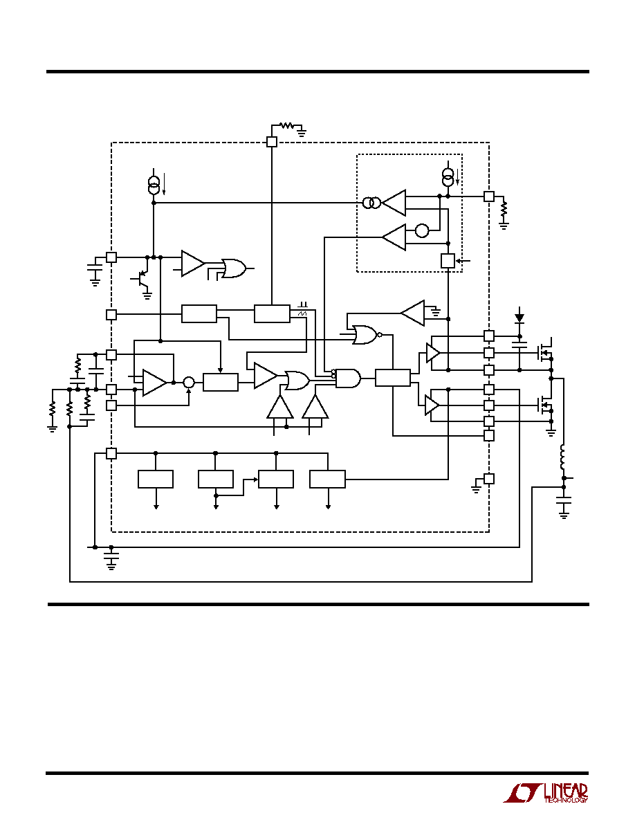
FU CTIO AL DIAGRA
U
U
W
5
1
UVSD OTSD
CHIP
SD
1V
3.2V
4
µ
A
RUN/SS
BANDGAP
SYNC
DETECT
OVER
TEMP
V
CC
UVLO
OSC
% DC
LIMIT
DRIVE
LOGIC
+
+
+
+
EXT SYNC
FORCED CONTINUOUS
÷
+
+
+
+
+
0.8V
MODE/SYNC
3
COMP
4
FB
16
15
14
13
11
10
9
6
12
V
IN
V
CC
(<15V)
INV
PWM
MIN
MAX
0.76V
0.84V
±
OVERCURRENT
12
µ
A
50mV
I
MAX
R
MAX
BOOST
TG
SW
DRV
CC
BG
BGRTN
INV
8 GND
GN16
OT SD
0.8V
REFERENCE
INTERNAL
3.2V V
CC
UV SD
2
FSET
3703 FD
REVERSE
CURRENT
FB
RSET
5
C
SS
R2
R1
V
CC
C
VCC
D
B
C
B
V
CC
V
IN
M1
M2
C
OUT
V
OUT
L1
INV
±
OPERATIO
U
The LTC3703 is a constant frequency, voltage mode
controller for DC/DC step-down converters. It is designed
to be used in a synchronous switching architecture with
two external N-channel MOSFETs. Its high operating volt-
age capability allows it to directly step down input voltages
up to 100V without the need for a step-down transformer.
For circuit operation, please refer to the Functional Dia-
gram of the IC and Figure 1. The LTC3703 uses voltage
mode control in which the duty ratio is controlled directly
by the error amplifier output and thus requires no current
sense resistor. The V
FB
pin receives the output voltage
feedback and is compared to the internal 0.8V reference by
the error amplifier, which outputs an error signal at the
COMP pin. When the load current increases, it causes a
drop in the feedback voltage relative to the reference. The
COMP voltage then rises, increasing the duty ratio until the
(Refer to Functional Diagram)
LTC3703
9
3703f
OPERATIO
U
output feedback voltage again matches the reference
voltage. In normal operation, the top MOSFET is turned on
when the RS latch is set by the on-chip oscillator and is
turned off when the PWM comparator trips and resets the
latch. The PWM comparator trips at the proper duty ratio
by comparing the error amplifier output (after being "com-
pensated" by the line feedforward multiplier) to a sawtooth
waveform generated by the oscillator. When the top
MOSFET is turned off, the bottom MOSFET is turned on
until the next cycle begins or, if Pulse Skip Mode operation
is enabled, until the inductor current reverses as deter-
mined by the reverse current comparator. MAX and MIN
comparators ensure that the output never exceed
±
5% of
nominal value by monitoring V
FB
and forcing the output
back into regulation quickly by either keeping the top
MOSFET off or forcing maximum duty cycle. The opera-
tion of its other features--fast transient response, out-
standing line regulation, strong gate drivers, short-circuit
protection, and shutdown/soft-start--are described be-
low.
Fast Transient Response
The LTC3703 uses a fast 25MHz op amp as an error
amplifier. This allows the compensation network to be
optimized for better load transient response. The high
bandwidth of the amplifier, along with high switching
frequencies and low value inductors, allow very high loop
crossover frequencies. The 800mV internal reference al-
lows regulated output voltages as low as 800mV without
external level shifting amplifiers.
Line Feedforward Compensation
The LTC3703 achieves outstanding line transient response
using a patented feedforward correction scheme. With
this circuit the duty cycle is adjusted instantaneously to
changes in input voltage, thereby avoiding unacceptable
overshoot or undershoot. It has the added advantage of
making the DC loop gain independent of input voltage.
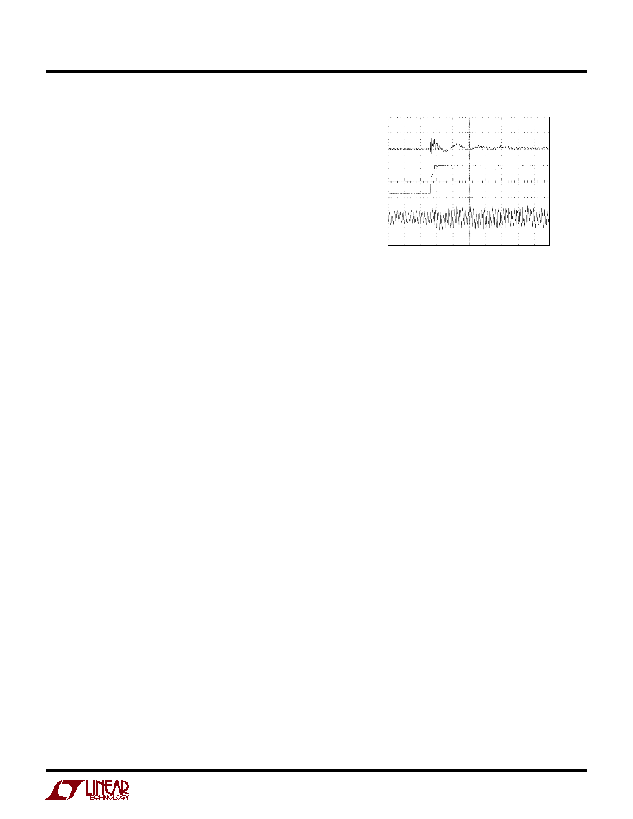
Figure 2 shows how large transient steps at the input have
little effect on the output voltage.
(Refer to Functional Diagram)
Strong Gate Drivers
The LTC3703 contains very low impedance drivers ca-
pable of supplying amps of current to slew large MOSFET
gates quickly. This minimizes transition losses and allows
paralleling MOSFETs for higher current applications. A
100V floating high side driver drives the top side MOSFET
and a low side driver drives the bottom side MOSFET (see
Figure 3). They can be powered from either a separate DC
supply or a voltage derived from the input or output
voltage (see MOSFET Driver Supplies section). The bot-
tom side driver is supplied directly from the DRV
CC
pin.
The top MOSFET drivers are biased from floating boot-
strap capacitor C
B
, which normally is recharged during
each off cycle through an external diode from DRV
CC
when
the top MOSFET turns off. In Pulse Skip Mode operation,
where it is possible that the bottom MOSFET will be off for
an extended period of time, an internal counter guarantees
that the bottom MOSFET is turned on at least once every
10 cycles for 10% of the period to refresh the bootstrap
capacitor. An undervoltage lockout keeps the LTC3703
shut down unless this voltage is above 9V.
The bottom driver has an additional feature that helps
minimize the possibility of external MOSFET shoot-thru.
When the top MOSFET turns on, the switch node dV/dt
pulls up the bottom MOSFET's internal gate through the
Miller capacitance, even when the bottom driver is holding
the gate terminal at ground. If the gate is pulled up high
enough, shoot-thru between the top side and bottom side
20
µ
s/DIV
V
OUT
50mV/DIV
V
OUT
= 12V
I
LOAD
= 1A
25V TO 60V V
IN
STEP
V
IN
20V/DIV
I
L
2A/DIV
3703 F02
Figure 2. Line Transient Performance
LTC3703
10
3703f
OPERATIO
U
MOSFETs can occur. To prevent this from occuring, the
bottom driver return is brought out as a separate pin
(BGRTN) so that a negative supply can be used to reduce
the effect of the Miller pull-up. For example, if a 2V supply
is used on BGRTN, the switch node dV/dt could pull the
gate up 2V before the V
GS
of the bottom MOSFET has more
than 0V across it.
cycle control set to 0%. As C
SS
continues to charge, the
duty cycle is gradually increased, allowing the output
voltage to rise. This soft-start scheme smoothly ramps the
output voltage to its regulated value, with no overshoot.
The RUN/SS voltage will continue ramping until it reaches
an internal 4V clamp. Then the MIN feedback comparator
is enabled and the LTC3703 is in full operation. When the
RUN/SS is low, the supply current is reduced to 50
µ
A.
CURRENT
LIMIT
NORMAL OPERATION
START-UP
0V
4V
3V
1.4V
1V
0V
POWER
DOWN MODE
MINIMUM
DUTY CYCLE
OUTPUT VOLTAGE
IN REGULATION
LTC3703
ENABLE
MIN COMPARATOR ENABLED
3703 F04
RUN/SS SOFT-STARTS
OUTPUT VOLTAGE AND
INDUCTOR CURRENT
SHUTDOWN
V
OUT
V
RUN/SS
(Refer to Functional Diagram)
BOOST
TG
SW
BG
BGRTN
DRV
CC
DRV
CC
LTC3703
MT
MB
+
+
V
IN
C
IN
V
OUT
C
OUT
D
B
C
B
L
3703 F03
0V TO 5V
Figure 4. Soft-Start Operation in Start Up and Current Limit
Figure 3. Floating TG Driver Supply and Negative BG Return
Constant Frequency
The internal oscillator can be programmed with an exter-
nal resistor connected from f
SET
to ground to run between
100kHz and 600kHz, thereby optimizing component size,
efficiency, and noise for the specific application. The
internal oscillator can also be synchronized to an external
clock applied to the MODE/SYNC pin and can lock to a
frequency in the 100kHz to 600kHz range. When locked to
an external clock, Pulse Skip Mode operation is automati-
cally disabled. Constant frequency operation brings with it
a number of benefits: Inductor and capacitor values can be
chosen for a precise operating frequency and the feedback
loop can be similarly tightly specified. Noise generated by
the circuit will always be at known frequencies.
Subharmonic oscillation and slope compensation, com-
mon headaches with constant frequency current mode
switchers, are absent in voltage mode designs like the
LTC3703.
Shutdown/Soft-Start
The main control loop is shut down by pulling RUN/SS pin
low. Releasing RUN/SS allows an internal 4
µ
A current
source to charge the soft-start capacitor C
SS
. When C
SS
reaches 1V, the main control loop is enabled with the duty
Current Limit
The LTC3703 includes an onboard current limit circuit that
limits the maximum output current to a user-programmed
level. It works by sensing the voltage drop across the
bottom MOSFET and comparing that voltage to a user-
programmed voltage at the I
MAX
pin. Since the bottom
MOSFET looks like a low value resistor during its on-time,
the voltage drop across it is proportional to the current
flowing in it. In a buck converter, the average current in the
inductor is equal to the output current. This current also
flows through the bottom MOSFET during its on-time.
Thus by watching the drain-to-source voltage when the
bottom MOSFET is on, the LTC3703 can monitor the
output current. The LTC3703 senses this voltage and
inverts it to allow it to compare the sensed voltage (which
becomes more negative as peak current increases) with a
positive voltage at the I
MAX
pin. The I
MAX
pin includes a
12
µ
A pull-up, enabling the user to set the voltage at I
MAX
with a single resistor (R
IMAX
) to ground. See the Current
Limit Programming section for R
IMAX
selection.
LTC3703
11
3703f
OPERATIO
U
For maximum protection, the LTC3703 current limit con-
sists of a steady-state limit circuit and an instantaneous
limit circuit. The steady-state limit circuit is a g
m
amplifier
that pulls a current from the RUN/SS pin proportional to
the difference between the SW and I
MAX
voltages. This
current begins to discharge the capacitor at RUN/SS,
reducing the duty cycle and controlling the output voltage
until the current regulates at the limit. Depending on the
size of the capacitor, it may take many cycles to discharge
the RUN/SS voltage enough to properly regulate the
output current. This is where the instantaneous limit
circuit comes into play. The instantaneous limit circuit is
a cycle-by-cycle comparator which monitors the bottom
MOSFET's drain voltage and keeps the top MOSFET from
turning on whenever the drain voltage is 50mV above the
programmed max drain voltage. Thus the cycle-by-cycle
comparator will keep the inductor current under control
until the g
m
amplifier gains control.
Pulse Skip Mode
The LTC3703 can operate in one of two modes selectable
with the MODE/SYNC pin--Pulse Skip Mode or forced
continuous mode. Pulse Skip Mode is selected when
increased efficiency at light loads is desired. In this mode,
the bottom MOSFET is turned off when inductor current
reverses to minimize the efficiency loss due to reverse
current flow. As the load is decreased (see Figure 6), the
duty cycle is reduced to maintain regulation until its
minimum on-time (~200ns) is reached. When the load
decreases below this point, the LTC3703 begins to skip
Figure 5. Efficiency in Pulse Skip/Forced Continuous Modes
LOAD (mA)
10
EFFICIENCY (%)
100
90
80
70
60
50
40
30
20
10
0
100
1000
10000
3703 F05
FORCED CONTINUOUS
PULSE SKIP MODE
V
IN
= 75V
V
IN
= 25V
V
IN
= 25V
V
IN
= 75V
cycles to maintain regulation. The frequency drops but
this further improves efficiency by minimizing gate charge
losses. In forced continuous mode, the bottom MOSFET is
always on when the top MOSFET is off, allowing the
inductor current to reverse at low currents. This mode is
less efficient due to resistive losses, but has the advantage
of better transient response at low currents, constant
frequency operation, and the ability to maintain regulation
when sinking current. See Figure 5 for a comparison of the
effect on efficiency at light loads for each mode. The
MODE/SYNC threshold is 0.8V
±
7.5%, allowing the MODE/
SYNC to act as a feedback pin for regulating a second
winding. If the feedback voltage drops below 0.8V, the
LTC3703 reverts to continuous operation to maintain
regulation in the secondary supply.
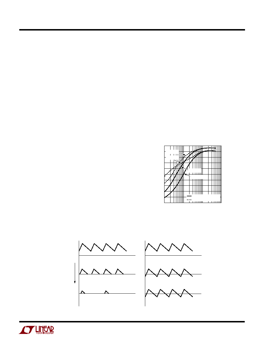
Figure 6. Comparison of Inductor Current Waveforms for Pulse Skip Mode and Forced Continuous Operation
PULSE SKIP MODE
FORCED CONTINUOUS
DECREASING
LOAD
CURRENT
3703 F06
LTC3703
12
3703f
The basic LTC3703 application circuit is shown in
Figure 1. External component selection is determined by
the input voltage and load requirements as explained in the
following sections. After the operating frequency is se-
lected, R
SET
and L can be chosen. The operating frequency
and the inductor are chosen for a desired amount of ripple
current and also to optimize efficiency and component
size. Next, the power MOSFETs and D1 are selected based
on voltage, load and efficiency requirements. C
IN
is se-
lected for its ability to handle the large RMS currents in the
converter and C
OUT
is chosen with low enough ESR to
meet the output voltage ripple and transient specifica-
tions. Finally, the loop compensation components are
chosen to meet the desired transient specifications.
Operating Frequency
The choice of operating frequency and inductor value is a
trade off between efficiency and component size. Low
frequency operation improves efficiency by reducing
MOSFET switching losses and gate charge losses. How-
ever, lower frequency operation requires more induc-
tance for a given amount of ripple current, resulting in a
larger inductor size and higher cost. If the ripple current
is allowed to increase, larger output capacitors may be
required to maintain the same output ripple. For convert-
ers with high step-down V
IN
to V
OUT
ratios, another
consideration is the minimum on-time of the LTC3703
(see the Minimum On-time Considerations section). A
final consideration for operating frequency is that in
APPLICATIO S I FOR ATIO
W
U
U
U
OPERATIO
U
noise-sensitive communications systems, it is often de-
sirable to keep the switching noise out of a sensitive
frequency band.
The LTC3703 uses a constant frequency architecture that
can be programmed over a 100kHz to 600kHz range with
a single resistor from the f
SET
pin to ground, as shown in
Figure 1. The nominal voltage on the f
SET
pin is 1.2V, and
the current that flows from this pin is used to charge and
discharge an internal oscillator capacitor. The value of
R
SET
for a given operating frequency can be chosen from
Figure 7 or from the following equation:
R
k
f kHz
SET
(
)
(
)
=
7100
25
Buck or Boost Mode Operation
The LTC3703 has the capability of operating both as a
step-down (buck) and step-up (boost) controller. In boost
mode, output voltages as high as 80V can be tightly
regulated. With the INV pin grounded, the LTC3703 oper-
ates in buck mode with TG driving the main (top side)
switch and BG driving the synchronous (bottom side)
switch. If the INV pin is pulled above 2V, the LTC3703
operates in boost mode with BG driving the main (bottom
side) switch and TG driving the synchronous (top side)
switch. Internal circuit operation is very similar regardless
of the operating mode with the following exceptions: In
boost mode, Pulse Skip Mode operation is always dis-
abled regardless of the level of the MODE/SYNC pin and
the line feedforward compensation is also disabled. The
overcurrent circuitry continues to monitor the load current
by looking at the drain voltage of the main (bottom side)
MOSFET. In boost mode, however, the peak MOSFET
current does not equal the load current but instead
I
D
= I
LOAD
/(1 D). This factor needs to be taken into
account when programming the I
MAX
voltage.
FREQUENCY (kHz)
R
SET
(k
)
1000
3703 F07
10
1
100
200
1000
800
600
400
0
Figure 7. Timing Resistor (R
SET
) Value
LTC3703
13
3703f
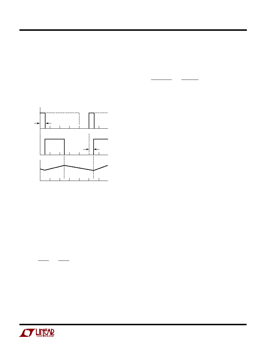
The oscillator can also be synchronized to an external
clock applied to the MODE/SYNC pin with a frequency in
the range of 100kHz to 600kHz (refer to the MODE/SYNC
Pin section for more details). In this synchronized mode,
Pulse Skip Mode operation is disabled. The clock high
level must exceed 2V for at least 25ns. As shown in
Figure 8, the top MOSFET turn-on will follow the rising
edge of the external clock by a constant delay equal to one-
tenth of the cycle period.
ripple current occurs at the highest V
IN
. To guarantee that
ripple current does not exceed a specified maximum, the
inductor in buck mode should be chosen according to:
L
V
f I
V
V
OUT
L MAX
OUT
IN MAX
(
)
(
)
1
The inductor also has an affect on low current operation
when Pulse Skip Mode operation is enabled. The fre-
quency begins to decrease when the output current drops
below the average inductor current at which the LTC3703
is operating at its t
ON(MIN)
in discontinuous mode (see
Figure 6). Lower inductance increases the peak inductor
current that occurs in each minimum on-time pulse and
thus increases the output current at which the frequency
starts decreasing.
Power MOSFET Selection
The LTC3703 requires at least two external N-channel
power MOSFETs, one for the top (main) switch and one or
more for the bottom (synchronous) switch. The number,
type and "on" resistance of all MOSFETs selected take into
account the voltage step-down ratio as well as the actual
position (main or synchronous) in which the MOSFET will
be used. A much smaller and much lower input capaci-
tance MOSFET should be used for the top MOSFET in
applications that have an output voltage that is less than
1/3 of the input voltage. In applications where V
IN
>> V
OUT
,
the top MOSFETs' "on" resistance is normally less impor-
tant for overall efficiency than its input capacitance at
operating frequencies above 300kHz. MOSFET manufac-
turers have designed special purpose devices that provide
reasonably low "on" resistance with significantly reduced
input capacitance for the main switch application in switch-
ing regulators.
Selection criteria for the power MOSFETs include the "on"
resistance R
DS(ON)
, input capacitance, breakdown voltage
and maximum output current.
The most important parameter in high voltage applica-
tions is breakdown voltage BV
DSS
. Both the top and
bottom MOSFETs will see full input voltage plus any
additional ringing on the switch node across its drain-to-
source during its off-time and must be chosen with the
3703 F08
2V TO 10V
MODE/
SYNC
TG
I
L
t
MIN
= 25ns
0.8T
0.1T
D = 40%
T
T = 1/f
O
APPLICATIO S I FOR ATIO
W
U
U
U
Figure 8. MODE/SYNC Clock Input and Switching
Waveforms for Synchronous Operation
Inductor
The inductor in a typical LTC3703 circuit is chosen for a
specific ripple current and saturation current. Given an
input voltage range and an output voltage, the inductor
value and operating frequency directly determine the
ripple current. The inductor ripple current in the buck
mode is:
=
I
V
f L
V
V
L
OUT
OUT
IN
( )( )
1
Lower ripple current reduces core losses in the inductor,
ESR losses in the output capacitors and output voltage
ripple. Thus highest efficiency operation is obtained at low
frequency with small ripple current. To achieve this how-
ever, requires a large inductor.
A reasonable starting point is to choose a ripple current
between 20% and 40% of I
O(MAX)
. Note that the largest
LTC3703
14
3703f
appropriate breakdown specification. Since many high
voltage MOSFETs have higher threshold voltages (typi-
cally, V
GS(MIN)
6V), the LTC3703 is designed to be used
with a 9V to 15V gate drive supply (DRV
CC
pin).
For maximum efficiency, on-resistance R
DS(ON)
and input
capacitance should be minimized. Low R
DS(ON)
minimizes
conduction losses and low input capacitance minimizes
transition losses. MOSFET input capacitance is a combi-
nation of several components but can be taken from the
typical "gate charge" curve included on most data sheets
(Figure 9).
The curve is generated by forcing a constant input current
into the gate of a common source, current source loaded
stage and then plotting the gate voltage versus time. The
initial slope is the effect of the gate-to-source and the gate-
to-drain capacitance. The flat portion of the curve is the
result of the Miller multiplication effect of the drain-to-gate
capacitance as the drain drops the voltage across the
current source load. The upper sloping line is due to the
drain-to-gate accumulation capacitance and the gate-to-
source capacitance. The Miller charge (the increase in
coulombs on the horizontal axis from a to b while the curve
is flat) is specified for a given V
DS
drain voltage, but can be
adjusted for different V
DS
voltages by multiplying by the
ratio of the application V
DS
to the curve specified V
DS
values. A way to estimate the C
MILLER
term is to take the
change in gate charge from points a and b on a manufac-
turers data sheet and divide by the stated V
DS
voltage
specified. C
MILLER
is the most important selection criteria
for determining the transition loss term in the top MOSFET
but is not directly specified on MOSFET data sheets. C
RSS
and C
OS
are specified sometimes but definitions of these
parameters are not included.
When the controller is operating in continuous mode the
duty cycles for the top and bottom MOSFETs are given by:
APPLICATIO S I FOR ATIO
W
U
U
U
MainSwitchDutyCycle
V
V
SynchronousSwitchDutyCycle
V
V
V
OUT
IN
IN
OUT
IN
=
=
The power dissipation for the main and synchronous
MOSFETs at maximum output current are given by:
P
D
I
D
R
V
I
D
R
C
V
V
V
f
P
D
I
R
MAIN
MAX
MAX
MAX
DR ON
OUT
MAX
MAX
DR
MILLER
CC
TH IL
TH IL
SYNC
MAX
MAX
DS N
=
+
+
+
=
+
1
1
1
2
1
1
1
1
1
1
2
2
2
0
(
)
(
)(
)·
( )
(
) (
)
(
)
( )
( )
(
)
where
is the temperature dependency of R
DS(ON)
, R
DR
is
the effective top driver resistance (approximately 2
at
V
GS
= V
MILLER
), V
IN
is the drain potential
and the change
in drain potential in the particular application. V
TH(IL)
is the
data sheet specified typical gate threshold voltage speci-
fied in the power MOSFET data sheet at the specified drain
current. C
MILLER
is the calculated capacitance using the
gate charge curve from the MOSFET data sheet and the
technique described above.
Both MOSFETs have I
2
R losses while the topside N-channel
equation includes an additional term for transition losses,
which peak at the highest input voltage. For V
IN
< 25V, the
high current efficiency generally improves with larger
MOSFETs, while for V
IN
> 25V, the transition losses
rapidly increase to the point that the use of a higher
R
DS(ON)
device with lower C
MILLER
actually provides higher
efficiency. The synchronous MOSFET losses are greatest
at high input voltage when the top switch duty factor is low
or during a short circuit when the synchronous switch is
on close to 100% of the period.
The term (1 +
) is generally given for a MOSFET in the
form of a normalized R
DS(ON)
vs temperature curve, and
typically varies from 0.005/
°
C to 0.01/
°
C depending on
the particular MOSFET used.
Figure 9. Gate Charge Characteristic
+
V
DS
V
IN
V
GS
MILLER EFFECT
Q
IN
a
b
C
MILLER
= (Q
B
Q
A
)/V
DS
V
GS
V
+
3703 F09
LTC3703
15
3703f
Multiple MOSFETs can be used in parallel to lower R
DS(ON)
and meet the current and thermal requirements if desired.
The LTC3703 contains large low impedance drivers ca-
pable of driving large gate capacitances without signifi-
cantly slowing transition times. In fact, when driving
MOSFETs with very low gate charge, it is sometimes
helpful to slow down the drivers by adding small gate
resistors (5
or less) to reduce noise and EMI caused by
the fast transitions.
Schottky Diode Selection
The Schottky diode D1 shown in Figure 1 conducts during
the dead time between the conduction of the power
MOSFETs. This prevents the body diode of the bottom
MOSFET from turning on and storing charge during the
dead time and requiring a reverse recovery period that
could cost as much as 1% to 2% in efficiency. A 1A
Schottky diode is generally a good size for 3A to 5A
regulators. Larger diodes result in additional losses due to
their larger junction capacitance. The diode can be omitted
if the efficiency loss can be tolerated.
Input Capacitor Selection
In continuous mode, the drain current of the top MOSFET
is approximately a square wave of duty cycle V
OUT
/V
IN
which must be supplied by the input capacitor. To prevent
large input transients, a low ESR input capacitor sized for
the maximum RMS current is given by:
I
I
V
V
V
V
CIN RMS
O MAX
OUT
IN
IN
OUT
(
)
(
)
/
1
1 2
This formula has a maximum at V
IN
= 2V
OUT
, where I
RMS
= I
O(MAX)
/2. This simple worst-case condition is com-
monly used for design because even significant deviations
do not offer much relief. Note that the ripple current ratings
from capacitor manufacturers are often based on only
2000 hours of life. This makes it advisable to further derate
the capacitor or to choose a capacitor rated at a higher
temperature than required. Several capacitors may also be
placed in parallel to meet size or height requirements in the
design.
Because tantalum and OS-CON capacitors are not avail-
able in voltages above 30V, for regulators with input
supplies above 30V, choice of input capacitor type is
limited to ceramics or aluminum electrolytics. Ceramic
capacitors have the advantage of very low ESR and can
handle high RMS current, however ceramics with high
voltage ratings (>50V) are not available with more than a
few microfarads of capacitance. Furthermore, ceramics
have high voltage coefficients which means that the ca-
pacitance values decrease even more when used at the
rated voltage. X5R and X7R type ceramics are recom-
mended for their lower voltage and temperature coeffi-
cients. Another consideration when using ceramics is
their high Q which if not properly damped, may result in
excessive voltage stress on the power MOSFETs. Alumi-
num electrolytics have much higher bulk capacitance,
however, they have higher ESR and lower RMS current
ratings.
A good approach is to use a combination of aluminum
electrolytics for bulk capacitance and ceramics for low
ESR and RMS current. If the RMS current cannot be
handled by the aluminum capacitors alone, when used
together, the percentage of RMS current that will be
supplied by the aluminum capacitor is reduced to approxi-
mately:
%
(
)
·
%
,
I
fCR
RMS ALUM
ESR
+
1
1
8
100
2
where R
ESR
is the ESR of the aluminum capacitor and C is
the overall capacitance of the ceramic capacitors. Using an
aluminum electrolytic with a ceramic also helps damp the
high Q of the ceramic, minimizing ringing.
Output Capacitor Selection
The selection of C
OUT
is primarily determined by the ESR
required to minimize voltage ripple. The output ripple
(
V
OUT
) is approximately equal to:
+
V
I ESR
fC
OUT
L
OUT
1
8
APPLICATIO S I FOR ATIO
W
U
U
U

LTC3703
16
3703f
Since
I
L
increases with input voltage, the output ripple is
highest at maximum input voltage. ESR also has a signifi-
cant effect on the load transient response. Fast load
transitions at the output will appear as voltage across the
ESR of C
OUT
until the feedback loop in the LTC3703 can
change the inductor current to match the new load current
value. Typically, once the ESR requirement is satisfied the
capacitance is adequate for filtering and has the required
RMS current rating.
Manufacturers such as Nichicon, United Chemicon and
Sanyo should be considered for high performance
throughhole capacitors. The OS-CON (organic semicon-
ductor dielectric) capacitor available from Sanyo has the
lowest product of ESR and size of any aluminum electro-
lytic at a somewhat higher price. An additional ceramic
capacitor in parallel with OS-CON capacitors is recom-
mended to reduce the effect of their lead inductance.
In surface mount applications, multiple capacitors placed
in parallel may be required to meet the ESR, RMS current
handling and load step requirements. Dry tantalum, spe-
cial polymer and aluminum electrolytic capacitors are
available in surface mount packages. Special polymer
capacitors offer very low ESR but have lower capacitance
density than other types. Tantalum capacitors have the
highest capacitance density but it is important to only use
types that have been surge tested for use in switching
power supplies. Several excellent surge-tested choices
are the AVX TPS and TPSV or the KEMET T510 series.
Aluminum electrolytic capacitors have significantly higher
ESR, but can be used in cost-driven applications providing
that consideration is given to ripple current ratings and
long term reliability. Other capacitor types include
Panasonic SP and Sanyo POSCAPs.
Output Voltage
The LTC3703 output voltage is set by a resistor divider
according to the following formula:
V
V
R
R
OUT
=
+
0 8
1
1
2
.
The external resistor divider is connected to the output as
shown in the Functional Diagram, allowing remote voltage
sensing. The resultant feedback signal is compared with
the internal precision 800mV voltage reference by the
error amplifier. The internal reference has a guaranteed
tolerance of
±
1%. Tolerance of the feedback resistors will
add additional error to the output voltage. 0.1% to 1%
resistors are recommended.
MOSFET Driver Supplies (DRV
CC
and BOOST)
The LTC3703 drivers are supplied from the DRV
CC
and
BOOST pins (see Figure 3), which have an absolute
maximum voltage of 15V. If the main supply voltage, V
IN
,
is higher than 15V a separate supply with a voltage
between 9V and 15V must be used to power the drivers. If
a separate supply is not available, one can easily be
generated from the main supply using one of the circuits
shown in Figure 10. If the output voltage is between 10V
and 15V, the output can be used to directly power the
drivers as shown in Figure 10a. If the output is below 10V,
Figure 10b shows an easy way to boost the supply voltage
to a sufficient level. This boost circuit uses the LT1613 in
a ThinSOT
TM
package and a chip inductor for minimal extra
area (<0.2 in
2
). Two other possible schemes are an extra
winding on the inductor (Figure 10c) or a capacitive
charge pump (Figure 10d). All the circuits shown in
Figure 10 require a start-up circuit (Q1, D1 and R1) to
provide driver power at initial start-up or following a short-
circuit. The resistor R1 must be sized so that it supplies
sufficient base current and zener bias current at the lowest
expected value of V
IN
. When using an existing supply, the
supply must be capable of supplying the required gate
driver current which can be estimated from:
I
DRVCC
= (f)(Q
G(TOP)
+ Q
G(BOTTOM)
)
This equation for I
DRVCC
is also useful for properly sizing
the circuit components shown in Figure 10.
An external bootstrap capacitor, C
B
, connected to the
BOOST pin supplies the gate drive voltage for the topside
MOSFETs. Capacitor C
B
is charged through external
diode, D
B
, from the DRV
CC
supply when SW is low. When
the top side MOSFET is turned on, the driver places the C
B
voltage across the gate-source of the top MOSFET. The
switch node voltage, SW, rises to V
IN
and the BOOST pin
follows. With the topside MOSFET on, the boost voltage
APPLICATIO S I FOR ATIO
W
U
U
U
LTC3703
17
3703f
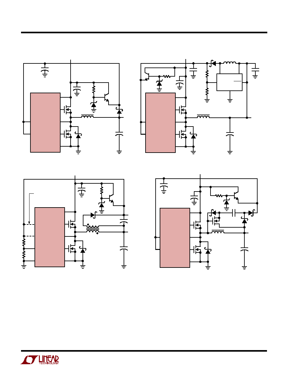
Figure 10a. V
CC
Generated from 10V < V
OUT
< 15V
APPLICATIO S I FOR ATIO
W
U
U
U
V
CC
DRV
CC
V
IN
TG
SW
BG
BGRTN
LTC3703
V
OUT
10V TO
15V
+
C
OUT
3703 F10a
+
C
IN
+
1
µ
F
V
IN
L1
12V
V
CC
DRV
CC
V
IN
TG
SW
BG
BGRTN
LTC3703
V
OUT
<10V
+
C
OUT
3703 F10b
+
C
IN
C9
4.7
µ
F
6.3V
V
IN
L1
12V
C10
1
µ
F
16V
V
IN
SW
GND
SHDN
FB
R17
1M
1%
R17
110k
1%
LT1613
D2
ZHCS400
L2
10
µ
H
Figure 10b. V
CC
Generated from V
OUT
< 10V
is above the input supply: V
BOOST
= V
IN
+ V
DRVCC
. The
value of the boost capacitor C
B
needs to be 100 times that
of the total input capacitance of the top side MOSFET(s).
The reverse breakdown of the external diode, D
B
, must be
greater than V
IN(MAX)
. Another important consideration
for the external diode is the reverse recovery and reverse
leakage, either of which may cause excessive reverse
current to flow at full reverse voltage. If the reverse
current times reverse voltage exceeds the maximum
V
CC
DRV
CC
FCB
GND
V
IN
TG1
SW
BG1
BGRTN
LTC3703
V
OUT
V
SEC
+
C
OUT
+
1
µ
F
3703 F10c
R1
V
IN
T1
OPTIONAL V
CC
CONNECTION
10V < V
SEC
< 15V
R2
+
C
IN
12V
N
1
V
CC
DRV
CC
V
IN
TG
SW
BG
BGRTN
LTC3703
V
OUT
+
C
OUT
3703 F10d
+
+
C
IN
V
IN
(<40V)
L1
1
µ
F
12V
BAT85
BAT85
BAT85
VN2222LL
0.22
µ
F
Figure 10c. Secondary Output Loop and V
CC
Connection
Figure 10d. Capacitive Charge Pump for V
CC
(V
IN
< 40V)
allowable power dissipation, the diode may be damaged.
For best results, use an ultrafast recovery silicon diode
such as the BAS21.
An internal undervoltage lockout (UVLO) monitors the
voltage on DRV
CC
to ensure that the LTC3703 has suffi-
cient gate drive voltage. If the DRV
CC
voltage falls below
the UVLO threshold, the LTC3703 shuts down and the gate
drive outputs remain low.

LTC3703
18
3703f
Bottom MOSFET Source Supply (BGRTN)
The bottom gate driver, BG, switches from DRV
CC
to BGRTN
where BGRTN can be a voltage between ground and 5V.
Why not just keep it simple and always connect BGRTN to
ground? In high voltage switching converters, the switch
node dV/dt can be many volts/ns, which will pull up on the
gate of the bottom MOSFET through its Miller capacitance.
If this Miller current, times the internal gate resistance of
the MOSFET plus the driver resistance, exceeds the thresh-
old of the FET, shoot-through will occur. By using a nega-
tive supply on BGRTN, the BG can be pulled below ground
when turning the bottom MOSFET off. This provides a few
extra volts of margin before the gate reaches the turn-on
threshold of the MOSFET. Be aware that the maximum
voltage difference between DRV
CC
and BGRTN is 15V. If,
for example, V
BGRTN
= 2V, the maximum voltage on
DRV
CC
pin is now 13V instead of 15V.
Current Limit Programming
Programming current limit on the LTC3703 is straight
forward. The I
MAX
pin sets the current limit by setting the
maximum allowable voltage drop across the bottom
MOSFET. The voltage across the MOSFET is set by its on-
resistance and the current flowing in the inductor, which
is the same as the output current. The LTC3703 current
limit circuit inverts the negative voltage across the MOSFET
before comparing it to the voltage at I
MAX
, allowing the
current limit to be set with a positive voltage.
To set the current limit, calculate the expected voltage
drop across the bottom MOSFET at the maximum desired
current and maximum junction temperature:
V
PROG
= (I
LIMIT
)(R
DS(ON)
)(1 +
)
where
is explained in the MOSFET Selection section.
V
PROG
is then programmed at the I
MAX
pin using the
internal 12
µ
A pull-up and an external resistor:
R
IMAX
= V
PROG
/12
µ
A
The current limit value should be checked to ensure that
I
LIMIT(MIN)
> I
OUT(MAX)
. The minimum value of current limit
generally occurs with the largest V
IN
at the highest ambi-
ent temperature, conditions that cause the largest power
loss in the converter. Note that it is important to check for
self-consistency between the assumed MOSFET junction
temperature and the resulting value of I
LIMIT
which heats
the MOSFET switches.
Caution should be used when setting the current limit
based upon the R
DS(ON)
of the MOSFETs. The maximum
current limit is determined by the minimum MOSFET on-
resistance. Data sheets typically specify nominal and
maximum values for R
DS(ON)
, but not a minimum. A
reasonable assumption is that the minimum R
DS(ON)
lies
the same amount below the typical value as the maximum
lies above it. Consult the MOSFET manufacturer for further
guidelines.
For best results, use a V
PROG
voltage between 100mV and
500mV. Values outside of this range may give less accu-
rate current limit. The current limit can also be disabled by
floating the I
MAX
pin.
FEEDBACK LOOP/COMPENSATION
Feedback Loop Types
In a typical LTC3703 circuit, the feedback loop consists of
the modulator, the external inductor, the output capacitor
and the feedback amplifier with its compensation network.
All of these components affect loop behavior and must be
accounted for in the loop compensation. The modulator
consists of the internal PWM generator, the output MOSFET
drivers and the external MOSFETs themselves. From a
feedback loop point of view, it looks like a linear voltage
transfer function from COMP to SW and has a gain roughly
equal to the input voltage. It has fairly benign AC behavior
at typical loop compensation frequencies with significant
phase shift appearing at half the switching frequency.
The external inductor/output capacitor combination makes
a more significant contribution to loop behavior. These
components cause a second order LC roll off at the output,
with the attendant 180
°
phase shift. This rolloff is what
filters the PWM waveform, resulting in the desired DC
output voltage, but the phase shift complicates the loop
compensation if the gain is still higher than unity at the
pole frequency. Eventually (usually well above the LC pole
frequency), the reactance of the output capacitor will
approach its ESR and the rolloff due to the capacitor
will stop, leaving 6dB/octave and 90
°
of phase shift
(Figure 11).
APPLICATIO S I FOR ATIO
W
U
U
U
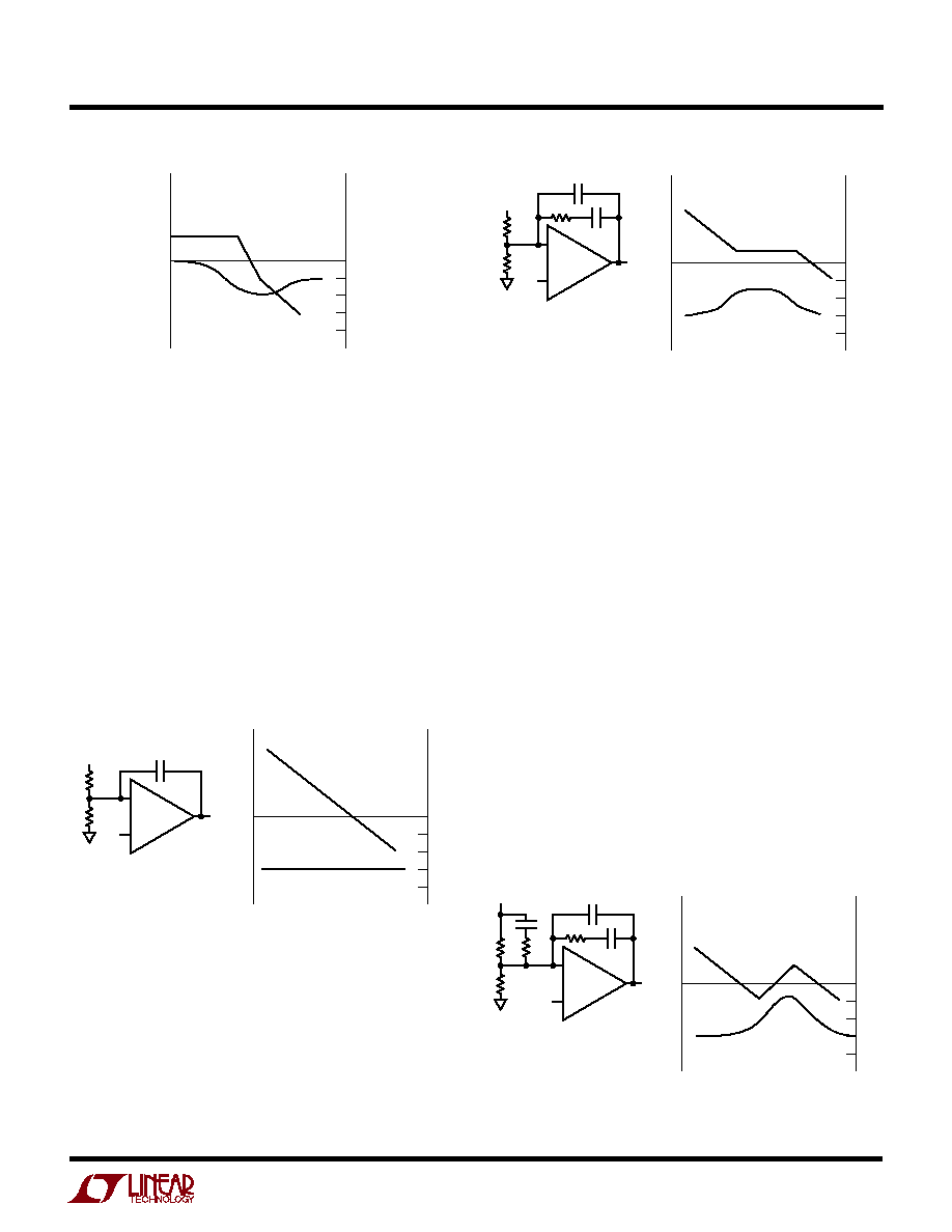
LTC3703
19
3703f
total phase shift due to the LC. The additional phase
compensation in the feedback amplifier allows the 0dB
point to be at or above the LC pole frequency, improving
loop bandwidth substantially over a simple Type 1 loop. It
has limited ability to compensate for LC combinations
where low capacitor ESR keeps the phase shift near 180
°
for an extended frequency range. LTC3703 circuits using
conventional switching grade electrolytic output capaci-
tors can often get acceptable phase margin with Type 2
compensation.
"Type 3" loops (Figure 14) use two poles and two zeros to
obtain a 180
°
phase boost in the middle of the frequency
band. A properly designed Type 3 circuit can maintain
acceptable loop stability even when low output capacitor
ESR causes the LC section to approach 180
°
phase shift
well above the initial LC roll-off. As with a Type 2 circuit,
the loop should cross through 0dB in the middle of the
phase bump to maximize phase margin. Many LTC3703
circuits using low ESR tantalum or OS-CON output capaci-
tors need Type 3 compensation to obtain acceptable phase
margin with a high bandwidth feedback loop.
So far, the AC response of the loop is pretty well out of the
user's control. The modulator is a fundamental piece of the
LTC3703 design and the external L and C are usually
chosen based on the regulation and load current require-
ments without considering the AC loop response. The
feedback amplifier, on the other hand, gives us a handle
with which to adjust the AC response. The goal is to have
180
°
phase shift at DC (so the loop regulates) and some-
thing less than 360
°
phase shift at the point that the loop
gain falls to 0dB. The simplest strategy is to set up the
feedback amplifier as an inverting integrator, with the 0dB
frequency lower than the LC pole (Figure 12). This "Type
1" configuration is stable but transient response is less
than exceptional if the LC pole is at a low frequency.
APPLICATIO S I FOR ATIO
W
U
U
U
GAIN (dB)
3703 F11
A
V
0
PHASE
6dB/OCT
12dB/OCT
GAIN
PHASE (DEG)
FREQ
90
180
270
360
Figure 11. Transfer Function of Buck Modulator
GAIN (dB)
3703 F12
0
PHASE
6dB/OCT
GAIN
PHASE (DEG)
FREQ
90
180
270
360
R
B
R1
FB
C1
IN
OUT
+
V
REF
Figure 12. Type 1 Schematic and Transfer Function
GAIN (dB)
3703 F13
0
PHASE
6dB/OCT
6dB/OCT
GAIN
PHASE (DEG)
FREQ
90
180
270
360
R
B
V
REF
R1
R2
FB
C2
IN
OUT
+
C1
Figure 13. Type 2 Schematic and Transfer Function
GAIN (dB)
3703 F14
0
PHASE
6dB/OCT
+6dB/OCT
6dB/OCT
GAIN
PHASE (DEG)
FREQ
90
180
270
360
R
B
V
REF
R1
R2
FB
C2
IN
OUT
+
C1
C3
R3
Figure 14. Type 3 Schematic and Transfer Function
Figure 13 shows an improved "Type 2" circuit that uses an
additional pole-zero pair to temporarily remove 90
°
of
phase shift. This allows the loop to remain stable with 90
°
more phase shift in the LC section, provided the loop
reaches 0dB gain near the center of the phase "bump."
Type 2 loops work well in systems where the ESR zero in
the LC roll-off happens close to the LC pole, limiting the

LTC3703
20
3703f
Feedback Component Selection
Selecting the R and C values for a typical Type 2 or Type 3
loop is a nontrivial task. The applications shown in this
data sheet show typical values, optimized for the power
components shown. They should give acceptable perfor-
mance with similar power components, but can be way off
if even one major power component is changed signifi-
cantly. Applications that require optimized transient re-
sponse will require recalculation of the compensation
values specifically for the circuit in question. The underly-
ing mathematics are complex, but the component values
can be calculated in a straightforward manner if we know
the gain and phase of the modulator at the crossover
frequency.
Modulator gain and phase can be measured directly from
a breadboard or can be simulated if the appropriate
parasitic values are known. Measurement will give more
accurate results, but simulation can often get close enough
to give a working system. To measure the modulator gain
and phase directly, wire up a breadboard with an LTC3703
and the actual MOSFETs, inductor and input and output
capacitors that the final design will use. This breadboard
should use appropriate construction techniques for high
speed analog circuitry: bypass capacitors located close to
the LTC3703, no long wires connecting components,
appropriately sized ground returns, etc. Wire the feedback
amplifier as a simple Type 1 loop, with a 10k resistor from
V
OUT
to FB and a 0.1
µ
F feedback capacitor from COMP to
FB. Choose the bias resistor (R
B
) as required to set the
desired output voltage. Disconnect R
B
from ground and
connect it to a signal generator or to the source output of
a network analyzer to inject a test signal into the loop.
Measure the gain and phase from the COMP pin to the
output node at the positive terminal of the output capaci-
tor. Make sure the analyzer's input is AC coupled so that
the DC voltages present at both the COMP and V
OUT
nodes
don't corrupt the measurements or damage the analyzer.
If breadboard measurement is not practical, a SPICE
simulation can be used to generate approximate gain/
phase curves. Plug the expected capacitor, inductor and
MOSFET values into the following SPICE deck and gener-
ate an AC plot of V(V
OUT
)/V(COMP) in dB and phase of
V
OUT
in degrees. Refer to your SPICE manual for details of
how to generate this plot.
APPLICATIO S I FOR ATIO
W
U
U
U
*3703 modulator gain/phase
*2003 Linear Technology
*this file written to run with PSpice 8.0
*may require modifications for other
SPICE simulators
*MOSFETs
rfet mod sw 0.02
;MOSFET rdson
*inductor
lext sw out1 10u
;inductor value
rl out1 out 0.015
;inductor series R
*output cap
cout out out2 540u
;capacitor value
resr out2 0 0.01
;capacitor ESR
*3703 internals
emod mod 0 value = {57*v(comp)}
;3703multiplier
vstim comp 0 0 ac 1
;ac stimulus
.ac dec 100 1k 1meg
.probe
.end
With the gain/phase plot in hand, a loop crossover fre-
quency can be chosen. Usually the curves look something
like Figure 11. Choose the crossover frequency in the
rising or flat parts of the phase curve, beyond the external
LC poles. Frequencies between 10kHz and 50kHz usually
work well. Note the gain (GAIN, in dB) and phase (PHASE,
in degrees) at this point. The desired feedback amplifier
gain will be -GAIN to make the loop gain at 0dB at this
frequency. Now calculate the needed phase boost, assum-
ing 60
°
as a target phase margin:
BOOST = (PHASE + 30
°
)
If the required BOOST is less than 60
°
, a Type 2 loop can
be used successfully, saving two external components.
BOOST values greater than 60
°
usually require Type 3
loops for satisfactory performance.
Finally, choose a convenient resistor value for R1 (10k is
usually a good value). Now calculate the remaining values:
(K is a constant used in the calculations)
f = chosen crossover frequency
G = 10
(GAIN/20)
(this converts GAIN in dB to G in
absolute gain)
LTC3703
21
3703f
TYPE 2 Loop:
TYPE 3 Loop:
APPLICATIO S I FOR ATIO
W
U
U
U
section. An example of a boost converter circuit is shown
in the Typical Applications section. To operate the LTC3703
in boost mode, the INV pin should be tied to the V
CC
voltage (or a voltage above 2V). Note that in boost mode,
pulse-skip operation and the line feedforward compensa-
tion are disabled.
For a boost converter, the duty cycle of the main switch is:
D
V
V
V
OUT
IN
OUT
=
For high V
OUT
to V
IN
ratios, the maximum V
OUT
is limited
by the LTC3703's maximum duty cycle which is typically
93%. The maximum output voltage is therefore:
V
V
D
V
OUT MAX
IN MIN
MAX
IN MIN
(
)
(
)
(
)
=
1
14
Boost Converter: Inductor Selection
In a boost converter, the average inductor current equals
the average input current. Thus, the maximum average
inductor current can be calculated from:
I
I
D
I
V
V
L MAX
O MAX
MAX
O MAX
O
IN MIN
(
)
(
)
(
)
(
)
·
=
-
=
1
Similar to a buck converter, choose the ripple current to be
20% to 40% of I
L(MAX)
. The ripple current amplitude then
determines the inductor value as follows:
L
V
I
f
D
IN MIN
L
MAX
=
(
)
·
·
The minimum required saturation current for the inductor
is:
I
L(SAT)
> I
L(MAX)
+
I
L
/2
Boost Converter: Power MOSFET Selection
For information about choosing power MOSFETs for a
boost converter, see the Power MOSFET Selection section
for the buck converter, since MOSFET selection is similar.
However, note that the power dissipation equations for the
MOSFETs at maximum output current in a boost converter
are:
K
BOOST
C
f G K R
C
C K
R
K
f C
R
V
R
V
V
B
REF
OUT
REF
=
+ °
=
=
-
( )
=
=
-
tan
· · · ·
· ·
( )
2
45
2
1
2
1
1
2
1
2
2
1
1
2
K
BOOST
C
f G R
C
C K
R
K
f C
R
R
K
C
f K R
R
V
R
V
V
B
REF
OUT
REF
=
+ °
=
=
-
( )
=
=
-
=
=
-
tan
· · ·
· ·
·
( )
2
4
45
2
1
2
1
1
2
1
2
2
1
3
1
1
3
1
2
3
1
Boost Converter Design
The following sections discuss the use of the LTC3703 as
a step-up (boost) converter. In boost mode, the LTC3703
can step-up output voltages as high as 80V. These sec-
tions discuss only the design steps specific to a boost
converter. For the design steps common to both a buck
and a boost, see the applicable section in the buck mode
LTC3703
22
3703f
Boost Converter: Output Capacitor Selection
In boost mode, the output capacitor requirements are
more demanding due to the fact that the current waveform
is pulsed instead of continuous as in a buck converter. The
choice of component(s) is driven by the acceptable ripple
voltage which is affected by the ESR, ESL and bulk
capacitance as shown in Figure 15. The total output ripple
voltage is:
=
+
V
I
f C
ESR
D
OUT
O MAX
OUT
MAX
(
)
·
1
1
where the first term is due to the bulk capacitance and
second term due to the ESR.
APPLICATIO S I FOR ATIO
W
U
U
U
discussion in Input Capacitor section for the buck con-
verter). With this combination, the ripple voltage can be
improved significantly. The low ESR ceremic capacitor
will minimize the ESR step, while the electrolytic will
supply the required bulk capacitance.
Boost Converter: Input Capacitor Selection
The input capacitor of a boost converter is less critical than
the output capacitor, due to the fact that the inductor is in
series with the input and the input current waveform is
continuous. The input voltage source impedance deter-
mines the size of the input capacitor, which is typically in
the range of 10
µ
F to 100
µ
F. A low ESR capacitor is
recommended though not as critical as for the output
capacitor.
The RMS input capacitor ripple current for a boost con-
verter is:
I
V
L f
D
RMS CIN
IN MIN
MAX
(
)
(
)
. ·
·
·
=
0 3
Please note that the input capacitor can see a very high
surge current when a battery is suddenly connected to the
input of the converter and solid tantalum capacitors can
fail catastrophically under these conditions. Be sure to
specify surge-tested capacitors!
Boost Converter: Current Limit Programming
The LTC3703 provides current limiting in boost mode by
monitoring the V
DS
of the main switch during its on-time
and comparing it to the voltage at I
MAX
. To set the current
limit, calculate the expected voltage drop across the
MOSFET at the maximum desired inductor current and
maximum junction temperature. The maximum inductor
current is a function of both duty cycle and maximum load
current, so the limit must be set for the maximum expected
duty cycle (minimum V
IN
) in order to ensure that the
current limit does not kick in at loads < I
O(MAX)
:
V
I
D
R
V
V
I
R
PROG
O MAX
MAX
DS ON
OUT
IN MIN
O MAX
DS ON
=
+
=
+
(
)
(
)
(
)
(
)
(
)
(
)
·
(
)
1
1
1
Figure 15. Output Voltage Ripple
Waveform for a Boost Converter
RINGING DUE TO
TOTAL INDUCTANCE
(BOARD + CAP)
V
ESR
V
COUT
V
OUT
(AC)
The choice of output capacitor is driven also by the RMS
ripple current requirement. The RMS ripple current is:
I
I
V
V
V
RMS COUT
O MAX
O
IN MIN
IN MIN
(
)
(
)
(
)
(
)
·
At lower output voltages (less than 30V), it may be
possible to satisfy both the output ripple voltage and RMS
ripple current requirements with one or more capacitors of
a single capacitor type. However, at output voltages above
30V where capacitors with both low ESR and high bulk
capacitance are hard to find, the best approach is to use a
combination of aluminum and ceramic capacitors (see
P
D
I
D
R
V
I
D
R
C
V
V
V
f
P
D
I
R
MAIN
MAX
MAX
MAX
DS ON
OUT
MAX
MAX
DR
MILLER
CC
TH IL
TH IL
SYNC
MAX
MAX
DS ON
=
+
( )
+
( )(
)
+
( )
=
( )
+
( )
1
1
1
2
1
1
1
1
1
1
2
2
2
·
(
)
( )
( )
(
)
LTC3703
23
3703f
Once V
PROG
is determined, R
IMAX
is chosen as follows:
R
IMAX
= V
PROG
/12
µ
A
Note that in a boost mode architecture, it is only possible
to provide protection for "soft" shorts where V
OUT
> V
IN
.
For hard shorts, the inductor current is limited only by the
input supply capability. Refer to Current Limit Program-
ming for buck mode for further considerations for current
limit programming.
Boost Converter: Feedback Loop/Compensation
Compensating a voltage mode boost converter is unfortu-
nately more difficult than for a buck converter. This is due
to an additional right-half plane (RHP) zero that is present
in the boost converter but not in a buck. The additional
phase lag resulting from the RHP zero is difficult if not
impossible to compensate even with a Type 3 loop, so the
best approach is usually to roll off the loop gain at a lower
frequency than what could be achievable in buck con-
verter.
A typical gain/phase plot of a voltage-mode boost con-
verter is shown in Figure 16. The modulator gain and
phase can be measured as described for a buck converter
or can be estimated as follows:
GAIN (COMP-to-V
OUT
DC gain) = 20Log(V
OUT
2
/V
IN
)
Dominant Pole: f
P
=
V
V
LC
IN
OUT
·
1
2
Since significant phase shift begins at frequencies above
the dominant LC pole, choose a crossover frequency no
greater than about half this pole frequency. The gain of the
compensation network should equal GAIN at this fre-
quency so that the overall loop gain is 0dB here. The
compensation component to achieve this, using a Type 1
amplifier (see Figure 12), is:
G = 10
GAIN/20
C1 = 1/(2
· f · G · R1)
Run/Soft-Start Function
The RUN/SS pin is a multipurpose pin that provide a soft-
start function and a means to shut down the LTC3703.
Soft-start reduces the input supply's surge current by
gradually increasing the duty cycle and can also be used
for power supply sequencing.
Pulling RUN/SS below 1V puts the LTC3703 into a low
quiescent current shutdown (I
Q
50
µ
A). This pin can be
driven directly from logic as shown in Figure 17. Releasing
the RUN/SS pin allows an internal 4
µ
A current source to
charge up the soft-start capacitor C
SS
. When the voltage
on RUN/SS reaches 1V, the LTC3703 begins operating at
its minimum on-time. As the RUN/SS voltage increases
from 1V to 3V, the duty cycle is allowed to increase from
0% to 100%. The duty cycle control minimizes input
supply inrush current and elimates output voltage over-
shoot at start-up and ensures current limit protection even
with a hard short. The RUN/SS voltage is internally clamped
at 4V.
Figure 16. Transfer Function of Boost Modulator
GAIN
(dB)
PHASE
(DEG)
3703 F16
A
V
0
0
90
180
PHASE
GAIN
12dB/OCT
Figure 17. LTC3703 Startup Operation
2ms/DIV
V
OUT
5V/DIV
V
IN
= 50V
I
LOAD
= 2A
C
SS
= 0.01
µ
F
RUN/SS
2V/DIV
I
L
2A/DIV
3703 F17
APPLICATIO S I FOR ATIO
W
U
U
U
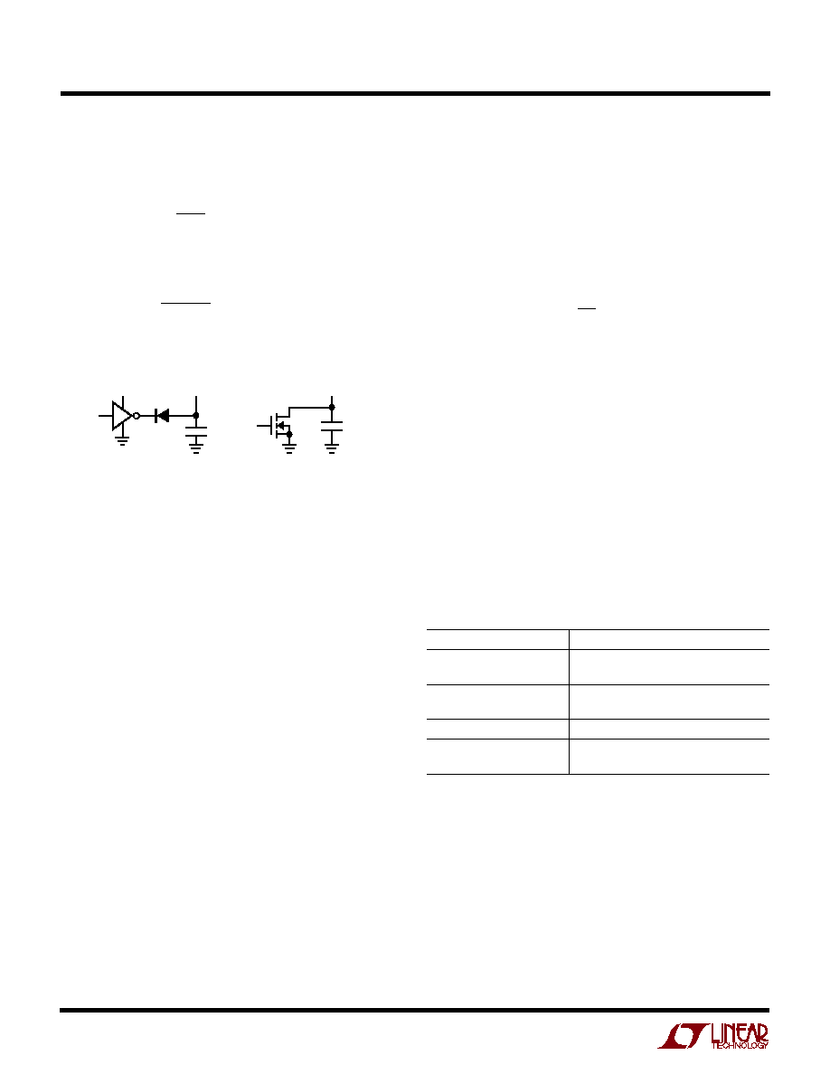
LTC3703
24
3703f
output remains heavy. To avoid this, the auxiliary output
voltage can be divided down with a conventional feedback
resistor string with the divided auxiliary output voltage fed
back to the MODE/SYNC pin. The MODE/SYNC threshold
is trimmed to 800mV with 20mV of hysteresis, allowing
precise control of the auxiliary voltage and is set as
follows:
V
V
R
R
SEC MIN
(
)
.
+
0 8
1
1
2
where R1 and R2 are shown in Figure 10c.
If the LTC3703 is operating in Pulse Skip Mode and the
auxiliary output voltage drops below V
SEC(MIN)
, the MODE/
SYNC pin will trip and the LTC3703 will resume continu-
ous operation regardless of the load on the main output.
Thus, the MODE/SYNC pin removes the requirement that
power must be drawn from the inductor primary in order
to extract power from the auxiliary winding. With the loop
in continuous mode (MODE/SYNC < 0.8V), the auxiliary
outputs may nominally be loaded without regard to the
primary output load.
The following table summarizes the possible states avail-
able on the MODE/SYNC pin:
Table 1.
MODE/SYNC Pin
Condition
DC Voltage: 0V to 0.75V
Forced Continuous
Current Reversal Enabled
DC Voltage:
0.87V
Pulse Skip Mode Operation
No Current Reversal
Feedback Resistors
Regulating a Secondary Winding
Ext. Clock: 0V to
2V
Forced Continuous
No Current Reversal
MODE/SYNC Pin (External Synchronization)
The internal LTC3703 oscillator can be synchronized to an
external oscillator by applying and clocking the MODE/
SYNC pin with a signal above 2V
P-P
. The internal oscillator
locks to the external clock after the second clock transition
is received. When external synchronization is detected,
LTC3703 will operate in forced continuous mode. If an
external clock transition is not detected for three succes-
sive periods, the internal oscillator will revert to the
frequency programmed by the R
SET
resistor. The internal
If RUN/SS starts at 0V, the delay before starting is approxi-
mately:
t
V
A
C
s
F C
DELAY START
SS
SS
,
( .
/
)
=
µ
=
µ
1
4
0 25
plus an additional delay, before the output will reach its
regulated value, of:
t
V
V
A
C
s
F C
DELAY REG
SS
SS
,
( .
/
)
µ
=
µ
3
1
4
0 5
The start delay can be reduced by using diode D1 in
Figure 18.
Figure 18. RUN/SS Pin Interfacing
MODE/SYNC Pin (Operating Mode and Secondary
Winding Control)
The MODE/SYNC pin is a dual function pin that can be used
for enabling or disabling Pulse Skip Mode operation and
also as an external clock input for synchronizing the
internal oscillator (see next section). Pulse Skip Mode is
enabled when the MODE/SYNC pin is above 0.8V and is
disabled, i.e. forced continuous, when the pin is below
0.8V.
In addition to providing a logic input to force continuous
operation and external synchronization, the MODE/SYNC
pin provides a means to regulate a flyback winding output
as shown in Figure 10c. The auxiliary output is taken from
a second winding on the core of the inductor, converting
it to a transformer. The auxiliary output voltage is set by
the main output voltage and the turns ratio of the extra
winding to the primary winding as follows:
V
SEC
(N + 1)V
OUT
Since the secondary winding only draws current when the
synchronous switch is on, load regulation at the auxiliary
output will be relatively good as long as the main output is
running in continuous mode. As the load on the primary
output drops and the LTC3703 switches to Pulse Skip
Mode operation, the auxiliary output may not be able to
maintain regulation, especially if the load on the auxiliary
APPLICATIO S I FOR ATIO
W
U
U
U
3.3V
OR 5V
RUN/SS
D1
C
SS
3703 F18
RUN/SS
C
SS

LTC3703
25
3703f
oscillator can synchronize to frequencies between 100kHz
and 600kHz, independent of the frequency programmed
by the R
SET
resistor. However, it is recommended that an
R
SET
resistor be chosen such that the frequency pro-
grammed by the R
SET
resistor is close to the expected
frequency of the external clock. In this way, the best
converter operation (ripple, component stress, etc) is
achieved if the external clock signal is lost.
Minimum On-Time Considerations (Buck Mode)
Minimum on-time t
ON(MIN)
is the smallest amount of time
that the LTC3703 is capable of turning the top MOSFET on
and off again. It is determined by internal timing delays and
the amount of gate charge required to turn on the top
MOSFET. Low duty cycle applications may approach this
minimum on-time limit and care should be taken to ensure
that:
t
V
V
f
t
ON
OUT
IN
ON MIN
=
>
·
(
)
where t
ON(MIN)
is typically 200ns.
If the duty cycle falls below what can be accommodated by
the minimum on-time, the LTC3703 will begin to skip
cycles. The output will be regulated, but the ripple current
and ripple voltage will increase. If lower frequency opera-
tion is acceptable, the on-time can be increased above
t
ON(MIN)
for the same step-down ratio.
Pin Clearance/Creepage Considerations
The LTC3703 is available in two packages (GN16 and G28)
both with identical functionality. The GN16 package gives
the smallest size solution, however the 0.013" (minimum)
space between pins may not provide sufficient PC board
trace clearance between high and low voltage pins in
higher voltage applications. Where clearance is an issue,
the G28 package should be used. The G28 package has 4
unconnected pins between the all adjacent high voltage
and low voltage pins, providing 5(0.0106") = 0.053"
clearance which will be sufficient for most applications up
to 100V. For more information, refer to the printed circuit
board design standards described in IPC-2221
(www.ipc.org).
APPLICATIO S I FOR ATIO
W
U
U
U
Efficiency Considerations
The efficiency of a switching regulator is equal to the
output power divided by the input power (x100%). Per-
cent efficiency can be expressed as:
%Efficiency = 100% (L1 + L2 + L3 + ...)
where L1, L2, etc. are the individual losses as a percentage
of input power. It is often useful to analyze the individual
losses to determine what is limiting the efficiency and
what change would produce the most improvement. Al-
though all dissipative elements in the circuit produce
losses, four main sources usually account for most of the
losses in LTC3703 circuits: 1) LTC3703 V
CC
current, 2)
MOSFET gate current, 3) I
2
R losses, 4) Topside MOSFET
transition losses.
1. V
CC
Supply current. The V
CC
current is the DC supply
current given in the Electrical Characteristics table which
powers the internal control circuitry of the LTC3703. Total
supply current is typically about 2.5mA and usually results
in a small (<1%) loss which is proportional to V
CC
.
2. DRV
CC
current is MOSFET driver current. This current
results from switching the gate capacitance of the power
MOSFETs. Each time a MOSFET gate is switched on and
then off, a packet of gate charge Q
G
moves from DRV
CC
to
ground. The resulting dQ/dt is a current out of the DRV
CC
supply. In continuous mode, I
DRVCC
= f(Q
G(TOP)
+ Q
G(BOT)
),
where Q
G(TOP)
and Q
G(BOT)
are the gate charges of the top
and bottom MOSFETs.
3. I
2
R losses are predicted from the DC resistances of
MOSFETs, the inductor and input and output capacitor
ESR. In continuous mode, the average output current
flows through L but is "chopped" between the topside
MOSFET and the synchronous MOSFET. If the two
MOSFETs have approximately the same R
DS(ON)
, then the
resistance of one MOSFET can simply be summed with the
DCR resistance of L to obtain I
2
R losses. For example, if
each R
DS(ON)
= 25m
and R
L
= 25m
, then total resis-
tance is 50m
. This results in losses ranging from 1% to
5% as the output current increases from 1A to 5A for a 5V
output.
4. Transition losses apply only to the topside MOSFET in
buck mode and they become significant when operating at

LTC3703
26
3703f
higher input voltages (typically 20V or greater). Transition
losses can be estimated from the second term of the P
MAIN
equation found in the Power MOSFET Selection section.
The transition losses can become very significant at the
high end of the LTC3703 operating voltage range. To
improve efficiency, one may consider lowering the fre-
quency and/or using MOSFETs with lower C
RSS
at the
expense of higher R
DS(ON)
.
Other losses including C
IN
and C
OUT
ESR dissipative
losses, Schottky conduction losses during dead-time, and
inductor core losses generally account for less than 2%
total additional loss.
Transient Response
Due to the high gain error amplifier and line feedforward
compensation of the LTC3703, the output accuracy due to
DC variations in input voltage and output load current will
be almost negligible. For the few cycles following a load
transient, however, the output deviation may be larger
while the feedback loop is responding. Consider a typical
48V input to 5V output application circuit, subjected to a
1A to 5A load transient. Initially, the loop is in regulation
and the DC current in the output capacitor is zero. Sud-
denly, an extra 4A (= 5A-1A) flows out of the output
capacitor while the inductor is still supplying only 1A. This
sudden change will generate a (4A) · (R
ESR
) voltage step
at the output; with a typical 0.015
output capacitor ESR,
this is a 60mV step at the output.
The feedback loop will respond and will move at the band-
width allowed by the external compensation network
towards a new duty cycle. If the unity gain crossover fre-
quency is set to 50kHz, the COMP pin will get to 60% of the
way to 90% duty cycle in 3
µ
s. Now the inductor is seeing
43V across itself for a large portion of the cycle and its
current will increase from 1A at a rate set by di/dt = V/L. If
the inductor value is 10
µ
H, the peak di/dt will be 43V/10
µ
H
or 4.3A/
µ
s. Sometime in the next few micro-seconds after
the switch cycle begins, the inductor current will have
risen to the 5A level of the load current and the output
voltage will stop dropping. At this point, the inductor cur-
rent will rise somewhat above the level of the output cur-
rent to replenish the charge lost from the output capacitor
during the load transient. With a properly compensated
loop, the entire recovery time will be inside of 10
µ
s.
Most loads care only about the maximum deviation from
ideal, which occurs somewhere in the first two cycles after
the load step hits. During this time, the output capacitor
does all the work until the inductor and control loop regain
control. The initial drop (or rise if the load steps down) is
entirely controlled by the ESR of the capacitor and amounts
to most of the total voltage drop. To minimize this drop,
choose a low ESR capacitor and/or parallel multiple ca-
pacitors at the output. The capacitance value accounts for
the rest of the voltage drop until the inductor current rises.
With most output capacitors, several devices paralleled to
get the ESR down will have so much capacitance that this
drop term is negligible. Ceramic capacitors are an excep-
tion; a small ceramic capacitor can have suitably low ESR
with relatively small values of capacitance, making this
second drop term more significant.
Optimizing Loop Compensation
Loop compensation has a fundamental impact on tran-
sient recovery time, the time it takes the LTC3703 to
recover after the output voltage has dropped due to a load
step. Optimizing loop compensation entails maintaining
the highest possible loop bandwidth while ensuring loop
stability. The feedback component selection section de-
scribes in detail the techniques used to design an opti-
mized Type 3 feedback loop, appropriate for most LTC3703
systems.
Measurement Techniques
Measuring transient response presents a challenge in two
respects: obtaining an accurate measurement and gener-
ating a suitable transient to test the circuit. Output mea-
surements should be taken with a scope probe directly
across the output capacitor. Proper high frequency prob-
ing techniques should be used. In particular, don't use the
6" ground lead that comes with the probe! Use an adapter
that fits on the tip of the probe and has a short ground clip
to ensure that inductance in the ground path doesn't cause
a bigger spike than the transient signal being measured.
Conveniently, the typical probe tip ground clip is spaced
just right to span the leads of a typical output capacitor.
Now that we know how to measure the signal, we need to
have something to measure. The ideal situation is to use
the actual load for the test and switch it on and off while
APPLICATIO S I FOR ATIO
W
U
U
U
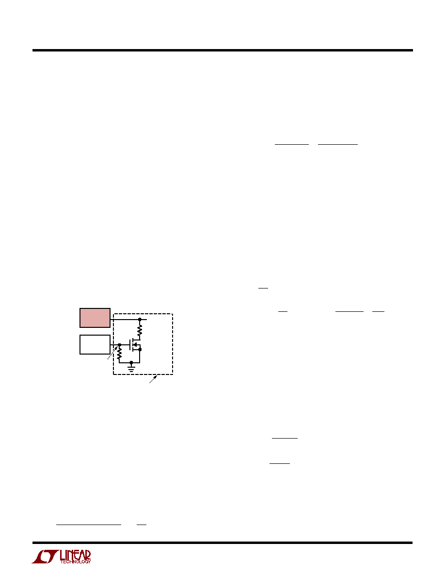
LTC3703
27
3703f
watching the output. If this isn't convenient, a current step
generator is needed. This generator needs to be able to
turn on and off in nanoseconds to simulate a typical
switching logic load, so stray inductance and long clip
leads between the LTC3703 and the transient generator
must be minimized.
Figure 19 shows an example of a simple transient genera-
tor. Be sure to use a noninductive resistor as the load
element--many power resistors use an inductive spiral
pattern and are not suitable for use here. A simple solution
is to take ten 1/4W film resistors and wire them in parallel
to get the desired value. This gives a noninductive resistive
load which can dissipate 2.5W continuously or 50W if
pulsed with a 5% duty cycle, enough for most LTC3703
circuits. Solder the MOSFET and the resistor(s) as close to
the output of the LTC3703 circuit as possible and set up
the signal generator to pulse at a 100Hz rate with a 5% duty
cycle. This pulses the LTC3703 with 500
µ
s transients10ms
apart, adequate for viewing the entire transient recovery
time for both positive and negative transitions while keep-
ing the load resistor cool.
With 10
µ
H inductor, ripple current will vary from 3.2A to
4A (32% to 40%) over the input supply range.
Next, verify that the minimum on-time is not violated. The
minimum on-time occurs at maximum V
IN
:
t
V
V
f
kHz
ns
ON MIN
OUT
IN MIN
(
)
(
)
( )
(
)
=
=
=
12
72 250
667
which is above the LTC3703's 200ns minimum on-time.
Next, choose the top and bottom MOSFET switch. Since
the drain of each MOSFET will see the full supply voltage
72V(max) plus any ringing, choose a 100V MOSFET to
provide a margin of safety. Si7456DP has a 100V BV
DSS
,
R
DS(ON)
= 25m
(max),
= 0.009/
°
C, C
MILLER
= (19nC
10nC)/50V = 180pF, V
GS(MILLER)
= 4.7V,
JA
= 20
°
C/W.
The power dissipation can be estimated at maximum input
voltage, assuming a junction temperature of 100
°
C (30
°
C
above an ambient of 70
°
C):
P
pF
k
W
W
W
MAIN
=
+
[
]
+
+
=
+
=
12
72
10
1 0 009 100 25 0 025
72
10
2
2 180
1
10 4 7
1
4 7
250
0 70
0 94
1 64
2
2
( )
.
(
) ( .
)
( )
( )(
)·
.
.
(
)
.
.
.
And double check the assumed T
J
in the MOSFET:
T
J
= 70
°
C + (1.64W)(20
°
C/W) = 103
°
C
Since the synchronous MOSFET will be conducting over
twice as long each period (almost 100% of the period in
short circuit) as the top MOSFET, use two Si7456DP
MOSFETs on the bottom:
P
W
SYNC
=
-
+
[
]
=
72 12
72
10
1 0 009 100 25
0 025
2
1 74
2
( )
.
(
) ·
.
.
T
J
= 70
°
C + (1.74W)(20
°
C/W) = 105
°
C
Next, set the current limit resistor. Since I
MAX
= 10A, the
limit should be set such that the minimum current limit is
>10A. Minimum current limit occurs at maximum R
DS(ON)
.
APPLICATIO S I FOR ATIO
W
U
U
U
Figure 19. Transient Load Generator
LTC3703
V
OUT
IRFZ44 OR
EQUIVALENT
R
LOAD
50
0V TO 10V
100Hz, 5%
DUTY CYCLE
LOCATE CLOSE TO THE OUTPUT
3703 F19
PULSE
GENERATOR
Design Example
As a design example, take a supply with the following
specifications: V
IN
= 36V to 72V (48V nominal), V
OUT
=
12V
±
5%, I
OUT(MAX)
= 10A, f=250kHz. First, calculate R
SET
to give the 250kHz operating frequency:
R
SET
= 7100/(250-25) = 31.6k
Next, choose the inductor value for about 40% ripple
current at maximum V
IN
:
L
V
kHz
A
H
=
= µ
12
250
0 4 10
1
12
72
10
(
)( . )(
)

LTC3703
28
3703f
Using the above calculation for bottom MOSFET T
J
, the
max R
DS(ON)
= (25m
/2) [1 + 0.009 (105-25)] = 21.5m
Therefore, I
MAX
pin voltage should be set to (10A)(0.0215)
= 0.215V. The R
SET
resistor can now be chosen to be
0.215V/12
µ
A = 18k
.
C
IN
is chosen for an RMS current rating of about 5A (I
MAX
/
2) at 85
°
C. For the output capacitor, two low ESR OSCON
capacitors (18m
each) are used to minimize output
voltage changes due to inductor current ripple and load
steps. The ripple voltage will be:
V
OUT(RIPPLE)
=
I
L(MAX)
(ESR) = (4A)(0.018
/2)
= 36mV
However, a 0A to 10A load step will cause an output
voltage change of up to:
V
OUT(STEP)
=
I
LOAD(ESR)
= (10A)(0.009
)
= 90mV
PC Board Layout Checklist
When laying out the printed circuit board, the following
checklist should be used to ensure proper operation of the
LTC3703. These items are also illustrated graphically in
the layout diagram of Figure 18. For layout of a Boost Mode
Converter, layout is similar with V
IN
and V
OUT
swapped.
Check the following in your layout:
1. Keep the signal and power grounds separate. The signal
ground consists of the LTC3703 GND pin, the ground
return of C
VCC
, and the () terminal of V
OUT
. The power
ground consists of the Schottky diode anode, the source
of the bottom side MOSFET, and the () terminal of the
input capacitor and DRV
CC
capacitor. Connect the signal
and power grounds together at the () terminal of the
output capacitor. Also, try to connect the () terminal of
the output capacitor as close as possible to the ()
terminals of the input and DRV
CC
capacitor and away from
the Schottky loop described in (2).
2. The high di/dt loop formed by the top N-channel
MOSFET, the bottom MOSFET and the C
IN
capacitor
should have short leads and PC trace lengths to minimize
high frequency noise and voltage stress from inductive
ringing.
3. Connect the drain of the top side MOSFET directly to the
(+) plate of C
IN
, and connect the source of the bottom side
MOSFET directly to the () terminal of C
IN
. This capacitor
provides the AC current to the MOSFETs.
4. Place the ceramic C
DRVCC
decoupling capacitor imme-
diately next to the IC, between DRV
CC
and BGRTN. This
capacitor carries the MOSFET drivers' current peaks.
Likewise the C
B
capacitor should also be next to the IC
between BOOST and SW.
5. Place the small-signal components away from high
frequency switching nodes (BOOST, SW, TG, and BG). In
the layout shown in Figure 20, all the small signal compo-
nents have been placed on one side of the IC and all of the
power components have been placed on the other. This
also helps keep the signal ground and power ground
isolated.
6. A separate decoupling capacitor for the supply, V
CC
, is
useful with an RC filter between the DRV
CC
supply and V
CC
pin to filter any noise injected by the drivers. Connect this
capacitor close to the IC, between the V
CC
and GND pins
and keep the ground side of the V
CC
capacitor (signal
ground) isolated from the ground side of the DRV
CC
capacitor (power ground).
7. For optimum load regulation and true remote sensing,
the top of the output resistor divider should connect
independently to the top of the output capacitor (Kelvin
connection), staying away from any high dV/dt traces.
Place the divider resistors near the LTC3703 in order to
keep the high impedance FB node short.
APPLICATIO S I FOR ATIO
W
U
U
U
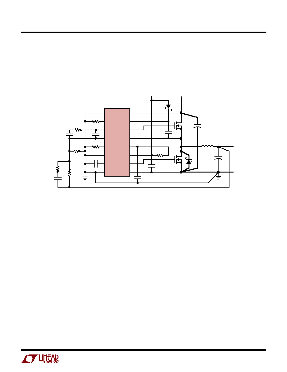
LTC3703
29
3703f
APPLICATIO S I FOR ATIO
W
U
U
U
Figure 20. LTC3703 Buck Converter Suggested Layout
LTC3703
MODE/SYNC
FSET
COMP
FB
I
MAX
INV
RUN/SS
GND
V
IN
BOOST
TG
SW
VCC
DRV
CC
BG
BGRTN
1
2
3
4
5
6
7
8
16
15
14
13
12
11
10
9
C
C1
C
IN
C
C2
C
C3
R
C1
R
C2
R1
R2
R
F
R
MAX
R
SET
C
B
V
IN
M1
M2
L1
D1
V
OUT
C
OUT
D
B
V
CC
C
SS
3703 F18
C
DRVCC
X5R
C
VCC
X5R
+
+
+
8. For applications with multiple switching power convert-
ers connected to the same input supply, make sure that the
input filter capacitor for the LTC3703 is not shared with
other converters. AC input current from another converter
could cause substantial input voltage ripple, and this could
interfere with the operation of the LTC3703. A few inches
of PC trace or wire (L
100nH) between C
IN
of the
LTC3703 and the actual source V
IN
should be sufficient to
prevent input noise interference problems.
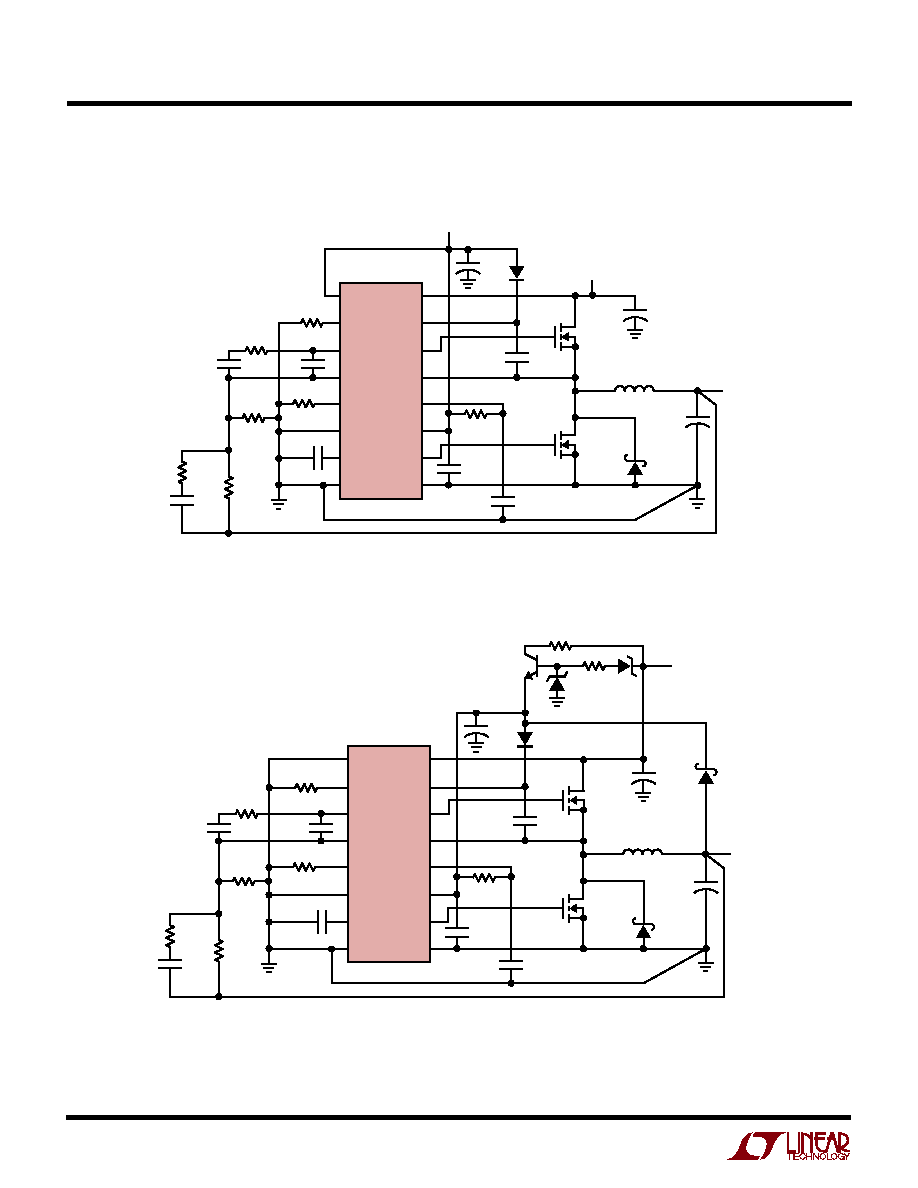
LTC3703
30
3703f
Single Input Supply 12V/5A Output Step-Down Converter
TYPICAL APPLICATIO S
U
36V-72V Input Voltage to 5V/10A Step-Down Converter with Pulse Skip Mode Enabled
LTC3703
MODE/SYNC
FSET
COMP
FB
I
MAX
INV
RUN/SS
GND
16
15
14
13
12
11
10
9
1
2
3
4
5
6
7
8
V
IN
BOOST
TG
SW
V
CC
DRV
CC
BG
BGRTN
C
IN
22
µ
F
100V
×
2
C
C2
100pF
C
C3
260pF
R
C1
120k
R
MAX
20k
C
C1
8pF
R
C2
3.2k
R1
42k
1%
R2
8.06k
1%
R
F
10
R
SET
25k
C
B
0.1
µ
F
V
IN
36V TO 72V
M2
Si7456DP
L1
4.7
µ
H
D1
MBR1100
V
OUT
5V
10A
C
OUT
220
µ
F
25V
×
2
D
B
BAS21
V
CC
9.3V TO 15V
C
SS
0.1
µ
F
3703 TA01
C
DRVCC
10
µ
F
C
VCC
1
µ
F
+
+
+
M1
Si7456DP
22
µ
F
25V
LTC3703
MODE/SYNC
FSET
COMP
FB
I
MAX
INV
RUN/SS
GND
V
IN
BOOST
TG
SW
V
CC
DRV
CC
BG
BGRTN
C
IN
22
µ
F
100V
×
2
V
IN
15V TO 80V
C
C2
3300pF
C
C3
1500pF
R
C1
22k
R
MAX
20k
C
C1
15pF
R
C2
330
*OPTIONAL ZENER PROVIDES UNDERVOLTAGE LOCKOUT ON INPUT SUPPLY, V
UVLO
10 + V
Z
R1
113k
1%
R2
8.06k
1%
R
F
10
R
SET
25k
C
B
0.1
µ
F
M2
Si7456DP
L1
15
µ
H
D1
MBR1100
V
OUT
12V
5A
C
OUT
220
µ
F
25V
×
2
D
B
BAS21
C
SS
0.1
µ
F
3703 TA02
C
DRVCC
10
µ
F
C
VCC
1
µ
F
+
+
+
M1
Si7456DP
22
µ
F
25V
FZT600
100
10k
*
12V
CMDSH-3
16
15
14
13
12
11
10
9
1
2
3
4
5
6
7
8
LTC3703
31
3703f
GN Package
16-Lead Plastic SSOP (Narrow .150 Inch)
(Reference LTC DWG # 05-08-1641)
GN16 (SSOP) 0502
1
2
3
4
5
6
7
8
.229 .244
(5.817 6.198)
.150 .157**
(3.810 3.988)
16 15 14 13
.189 .196*
(4.801 4.978)
12 11 10 9
.016 .050
(0.406 1.270)
.015
±
.004
(0.38
±
0.10)
×
45
°
0
°
8
°
TYP
.007 .0098
(0.178 0.249)
.053 .068
(1.351 1.727)
.008 .012
(0.203 0.305)
.004 .0098
(0.102 0.249)
.0250
(0.635)
BSC
.009
(0.229)
REF
.254 MIN
RECOMMENDED SOLDER PAD LAYOUT
.150 .165
.0250 TYP
.0165
±
.0015
.045
±
.005
*DIMENSION DOES NOT INCLUDE MOLD FLASH. MOLD FLASH
SHALL NOT EXCEED 0.006" (0.152mm) PER SIDE
**DIMENSION DOES NOT INCLUDE INTERLEAD FLASH. INTERLEAD
FLASH SHALL NOT EXCEED 0.010" (0.254mm) PER SIDE
INCHES
(MILLIMETERS)
NOTE:
1. CONTROLLING DIMENSION: INCHES
2. DIMENSIONS ARE IN
3. DRAWING NOT TO SCALE
U
PACKAGE DESCRIPTIO
G Package
28-Lead Plastic SSOP (5.3mm)
(Reference LTC DWG # 05-08-1640)
G28 SSOP 0802
0.09 0.25
(.0035 .010)
0
°
8
°
0.55 0.95
(.022 .037)
5.00 5.60**
(.197 .221)
7.40 8.20
(.291 .323)
1
2 3
4
5
6 7 8
9 10 11 12
14
13
9.90 10.50*
(.390 .413)
25
26
22 21 20 19 18 17 16 15
23
24
27
28
2.0
(.079)
0.05
(.002)
0.65
(.0256)
BSC
0.22 0.38
(.009 .015)
MILLIMETERS
(INCHES)
DIMENSIONS DO NOT INCLUDE MOLD FLASH. MOLD FLASH
SHALL NOT EXCEED .152mm (.006") PER SIDE
DIMENSIONS DO NOT INCLUDE INTERLEAD FLASH. INTERLEAD
FLASH SHALL NOT EXCEED .254mm (.010") PER SIDE
*
**
NOTE:
1. CONTROLLING DIMENSION: MILLIMETERS
2. DIMENSIONS ARE IN
3. DRAWING NOT TO SCALE
0.42
±
0.03
0.65 BSC
5.3 5.7
7.8 8.2
RECOMMENDED SOLDER PAD LAYOUT
1.25
±
0.12
Information furnished by Linear Technology Corporation is believed to be accurate and reliable.
However, no responsibility is assumed for its use. Linear Technology Corporation makes no represen-
tation that the interconnection of its circuits as described herein will not infringe on existing patent rights.
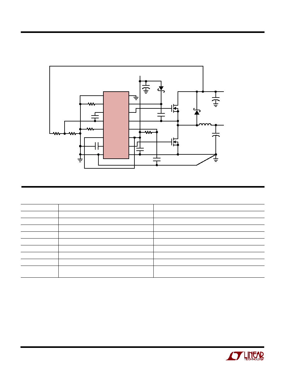
LTC3703
32
3703f
Linear Technology Corporation
1630 McCarthy Blvd., Milpitas, CA 95035-7417
(408) 432-1900
q
FAX: (408) 434-0507
q
www.linear.com
©
LINEAR TECHNOLOGY CORPORATION 2003
LT/TP 1203 1K · PRINTED IN USA
RELATED PARTS
TYPICAL APPLICATIO
U
PART NUMBER
DESCRIPTION
COMMENTS
LT1074HV/LT1076HV
Monolithic 5A/2A Step-Down DC/DC Converters
V
IN
up to 60V, TO-220 and DD Packages
LT1339
High Power Synchronous DC/DC Controller
V
IN
up to 60V, Drivers 10,000pF Gate Capacitance, I
OUT
20A
LTC1702A
Dual, 2-Phase Synchronous DC/DC Controller
550kHz Operation, No R
SENSE
, 3V
V
IN
7V, I
OUT
20A
LTC1735
Synchronous Step-Down DC/DC Controller
3.5V
V
IN
36V, 0.8V
V
OUT
6V, Current Mode, I
OUT
20A
LTC1778
No R
SENSE
Synchronous DC/DC Controller
4V
V
IN
36V, Fast Transient Response, Current Mode, I
OUT
20A
LT1956
Monolithic 1.5A, 500kHz Step-Down Regulator
5.5V
V
IN
60V, 2.5mA Supply Current, 16-Pin SSOP
LT3010
50mA, 3V to 80V Linear Regulator
1.275V
V
OUT
60V, No Protection Diode Required, 8-Lead MSOP
LT3430/LT3431
Monolithic 3A, 200kHz/500kHz Step-Down Regulator
5.5V
V
IN
60V, 0.1
Saturation Switch, 16-Pin SSOP
LT3433
Monolithic Step-Up/Step-Down DC/DC Converter
4V
V
IN
60V, 500mA Switch, Automatic Step-Up/Step-Down,
Single Inductor
5V to 12V/5A Synchronous Boost Converter
LTC3703
MODE/SYNC
FSET
COMP
FB
I
MAX
INV
RUN/SS
GND
V
IN
BOOST
TG
SW
V
CC
DRV
CC
BG
BGRTN
C
OUT
220
µ
F
16V
×
2
R
MAX
13k
C
C1
0.1
µ
F
R2
8.06k
1%
R
F
10
R1
113k
1%
R
SET
25k
C
B
0.1
µ
F
M2
Si7366DP
L1
3.3
µ
H
MBRS140T3
V
IN
3V TO 11V
V
OUT
12V
5A
C
IN
100
µ
F
16V
D
B
CMDSH-3
V
CC
9.3V TO 15V
C
SS
0.1
µ
F
3703 TA03
C
DRVCC
10
µ
F
C
VCC
1
µ
F
+
+
+
M1
Si7348DP
22
µ
F
25V
16
15
14
13
12
11
10
9
1
2
3
4
5
6
7
8