 | ÐлекÑÑоннÑй компоненÑ: LTC3718EG | СкаÑаÑÑ:  PDF PDF  ZIP ZIP |
3718fs
1
LTC3718
sn3718 3718fs
FEATURES
APPLICATIO S
U
DESCRIPTIO
U
TYPICAL APPLICATIO
U
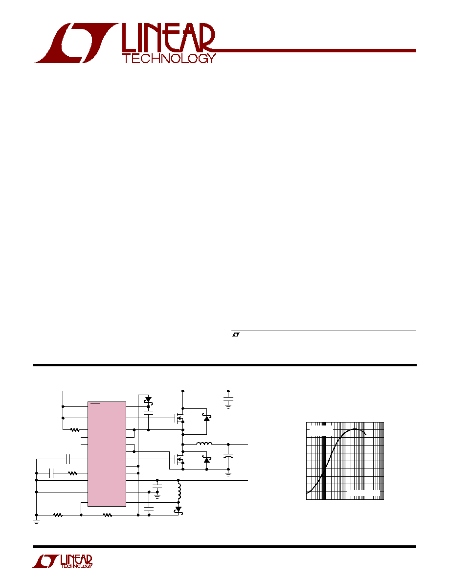
Low Input Voltage
DC/DC Controller for
DDR/QDR Memory Termination
s
Very Low V
IN(MIN)
: 1.5V
s
Ultrafast Transient Response
s
True Current Mode Control
s
5V Drive for N-Channel MOSFETs Eliminates
Auxillary 5V Supply
s
No Sense Resistor Required
s
Uses Standard 5V Logic-Level N-Channel MOSFETs
s
V
OUT(MIN)
: 0.4V
s
V
OUT
Tracks 1/2 V
IN
or External V
REF
s
Symmetrical Source and Sink Output Current Limit
s
Adjustable Switching Frequency
s
t
ON(MIN)
<100ns
s
Power Good Output Voltage Monitor
s
Programmable Soft-Start
s
Output Overvoltage Protection
s
Optional Short-Circuit Shutdown Timer
s
Small 24-Lead SSOP Package
s
Bus Termination: DDR/QDR Memory, SSTL, HSTL, ...
s
Servers, RAID Systems
s
Distributed Power Systems
s
Synchronous Buck with General Purpose Boost
The LTC
®
3718 is a high current, high efficiency synchro-
nous switching regulator controller for DDR and QDR
TM
memory termination. It operates from an input as low as
1.5V and provides a regulated output voltage equal to
(0.5)V
IN
. The controller uses a valley current control
architecture to enable high frequency operation with very
low on-times without requiring a sense resistor. Operating
frequency is selected by an external resistor and is com-
pensated for variations in V
IN
and V
OUT
. The LTC3718 uses
a pair of standard 5V logic level N-channel external
MOSFETs, eliminating the need for expensive P-channel
or low threshold devices.
Forced continuous operation reduces noise and RF inter-
ference. Fault protection is provided by internal foldback
current limiting, an output overvoltage comparator and an
optional short-circuit timer. Soft-start capability for sup-
ply sequencing can be accomplished using an external
timing capacitor. OPTI-LOOP
®
compensation allows the
transient response to be optimized over a wide range of
loads and output capacitors.
Efficiency vs Load Current
, LTC and LT are registered trademarks of Linear Technology Corporation.
OPTI-LOOP is a registered trademark of Linear Technology Corporation. No R
SENSE
is a
trademark of Linear Technology Corporation. QDR RAMs and Quad Data Rate RAMs comprise a
new family of products developed by Cypress Semiconductor, IDT and Micron Technology, Inc.
C
SS
0.1
µ
F
R
C
4.75k
LTC3718
C1 820pF X7R
R
ON
237k
R
F1
12.1k
C
OUT
: SANYO POSCAP 4TPB470M
L1: SUMIDA CEP125-0R8MC
L2: PANASONIC ELJPC4R7MF
R
F2
37.4k
C
IN2
4.7
µ
F
L2
4.7
µ
H
M2
Si7440DP
D2
B340A
3718 TA01
L1 0.8
µ
H
D3
MBR0520
C
VCC1
10
µ
F
C
B
0.33
µ
F
D
B
CMDSH-3
C
OUT
470
µ
F
×
2
M1
Si7440DP
V
IN
2.5V
V
OUT
1.25V
±
10A
V
IN
C
IN1
22
µ
F
×
2
D1
B340A
SHDN
BOOST
V
REF
TG
I
ON
SW1
V
FB1
SENSE
+
PGOOD
PGND1
RUN/SS
SENSE
I
TH
BG
SGND1
INTV
CC
SGND2
V
IN1
V
FB2
SW2
PGND2
V
IN2
10
24
9
23
7
22
8
V
OUT
21
1
18
3
17
5
16
6
15
11
14
12
13
19
20
+
Figure 1. High Efficiency Bus Termination Supply without Auxiliary 5V Supply
LOAD CURRENT (A)
EFFICIENCY (%)
100
90
80
70
60
50
40
30
20
10
0
0.01
1
10
100
3718 G05/TA01a
0.1
V
IN
= 2.5V
V
OUT
= 1.25V
FIGURE 1 CIRCUIT
2
LTC3718
sn3718 3718fs
(Note 1)
Input Supply Voltage (V
IN2
) .......................10V to 0.3V
Boosted Topside Driver Supply Voltage
(BOOST) ............................................... 42V to 0.3V
V
IN1
, I
ON
, SW1 Voltage ............................. 36V to 0.3V
RUN/SS, PGOOD Voltages ......................... 7V to 0.3V
V
ON
, V
REF
, V
RNG
Voltages .......(INTV
CC
+ 0.3V) to 0.3V
I
TH
, V
FB1
Voltages .................................... 2.7V to 0.3V
SW2 Voltage ............................................. 36V to 0.4V
V
FB2
Voltage ................................................. V
IN2
+ 0.3V
SHDN Voltage ......................................................... 10V
TG, BG, INTV
CC
Peak Currents .................................. 2A
TG, BG, INTV
CC
RMS Currents ............................ 50mA
Operating Ambient Temperature
Range (Note 4) ................................... 40
°
C to 85
°
C
Junction Temperature (Note 2) ............................ 125
°
C
Storage Temperature Range ................. 65
°
C to 150
°
C
Lead Temperature (Soldering, 10 sec).................. 300
°
C
ORDER PART
NUMBER
LTC3718EG
T
JMAX
= 125
°
C,
JA
= 130
°
C/ W
The
q
denotes specifications which apply over the full operating
temperature range, otherwise specifications are T
A
= 25
°
C. V
IN1
= 15V, V
IN2
= 1.5V unless otherwise noted.
ABSOLUTE AXI U RATI GS
W
W
W
U
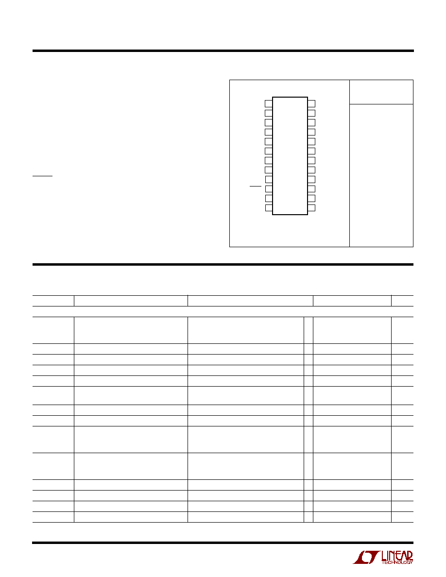
PACKAGE/ORDER I FOR ATIO
U
U
W
ELECTRICAL CHARACTERISTICS
1
2
3
4
5
6
7
8
9
10
11
12
TOP VIEW
G PACKAGE
24-LEAD PLASTIC SSOP
24
23
22
21
20
19
18
17
16
15
14
13
RUN/SS
V
ON
PGOOD
V
RNG
I
TH
SGND1
I
ON
V
FB1
V
REF
SHDN
SGND2
V
FB2
BOOST
TG
SW1
SENSE
+
SENSE
PGND1
BG
INTV
CC
V
IN1
V
IN2
PGND2
SW2
Consult LTC Marketing for parts specified with wider operating temperature ranges.
SYMBOL
PARAMETER
CONDITIONS
MIN
TYP
MAX
UNITS
Buck Regulator
I
Q(VIN1)
Input DC Supply Current (V
IN1
)
Normal
1000
2000
µ
A
Shutdown Supply Current
V
RUN/SS
= 0V
15
30
µ
A
V
FB1
Feedback Voltage Accuracy
I
TH
= 1.2V (Note 3)
q
0.65
0.1
0.65
%
V
FB1(LINE)
Feedback Voltage Line Regulation
V
IN1
= 4V to 36V, I
TH
= 1.2V (Note 3)
0.002
%/V
V
FB1(LOAD)
Feedback Voltage Load Regulation
I
TH
= 0.5V to 1.9V (Note 3)
q
0.05
0.3
%
g
m(EA)
Error Amplifier Transconductance
I
TH
= 1.2V (Note 3)
0.93
1.13
1.33
mS
t
ON
On-Time
I
ON
= 60
µ
A, V
ON
= 1.5V
200
250
300
ns
I
ON
= 30
µ
A, V
ON
= 1.5V
400
500
600
ns
t
ON(MIN)
Minimum On-Time
I
ON
= 180
µ
A
50
100
ns
t
OFF(MIN)
Minimum Off-Time
300
400
ns
V
SENSE(MAX)
Maximum Current Sense Threshold
V
RNG
= 1V, V
FB1
= V
REF
/2 50mV
q
108
135
162
mV
V
PGND
V
SW1
(Source)
V
RNG
= 0V, V
FB1
= V
REF
/2 50mV
q
76
95
114
mV
V
RNG
= INTV
CC
, V
FB1
= V
REF
/2 50mV
q
148
185
222
mV
V
SENSE(MIN)
Minimum Current Sense Threshold
V
RNG
= 1V, V
FB1
= V
REF
/2 + 50mV
140
165
190
mV
V
PGND
V
SW1
(Sink)
V
RNG
= 0V, V
FB1
= V
REF
/2 + 50mV
97
115
133
mV
V
RNG
= INTV
CC
, V
FB1
= V
REF
/2 + 50mV
200
235
270
mV
V
FB1(OV)
Output Overvoltage Fault Threshold
8
10
12
%
V
FB1(UV)
Output Undervoltage Fault Threshold
25
%
V
RUN/SS(ON)
RUN Pin Start Threshold
q
0.8
1.5
2
V
V
RUN/SS(LE)
RUN Pin Latchoff Enable
RUN/SS Pin Rising
4
4.5
V
3
LTC3718
sn3718 3718fs
The
q
denotes specifications which apply over the full operating
temperature range, otherwise specifications are T
A
= 25
°
C. V
IN1
= 15V, V
IN2
= 1.5V unless otherwise noted.
ELECTRICAL CHARACTERISTICS
SYMBOL
PARAMETER
CONDITIONS
MIN
TYP
MAX
UNITS
V
RUN/SS(LT)
RUN Pin Latchoff Threshold
RUN/SS Pin Falling
3.5
4.2
V
I
RUN/SS(C)
Soft-Start Charge Current
V
RUN/SS
= 0V
0.5
1.2
3
µ
A
I
RUN/SS(D)
Soft-Start Discharge Current
V
RUN/SS
= 4.5V, V
FB
= 0V
0.8
1.8
3
µ
A
V
IN(UVLO)
V
IN1
Undervoltage Lockout
V
IN
Falling
q
3.4
3.9
V
V
IN
Rising
q
3.5
4.0
V
TG R
UP
TG Driver Pull-Up On Resistance
TG High
2
3
TG R
DOWN
TG Driver Pull-Down On Resistance
TG Low
2
3
BG R
UP
BG Driver Pull-Up On Resistance
BG High
3
4
BG R
DOWN
BG Driver Pull-Down On Resistance
BG Low
1
2
TG t
r
TG Rise Time
C
LOAD
= 3300pF
20
ns
TG t
f
TG Fall Time
C
LOAD
= 3300pF
20
ns
BG t
r
BG Rise Time
C
LOAD
= 3300pF
20
ns
BG t
f
BG Fall Time
C
LOAD
= 3300pF
20
ns
Internal V
CC
Regulator
V
INTVCC
Internal V
CC
Voltage
6V < V
IN1
<30V
q
4.7
5
5.3
V
V
LDO(LOAD)
Internal V
CC
Load Regulation
I
CC
= 0mA to 20mA
0.1
±
2
%
PGOOD Output
V
FB1H
PGOOD Upper Threshold
V
FB1
= Rising
8
10
12
%
V
FB1L
PGOOD Lower Threshold
V
FB1
= Falling
8
10
12
%
V
FB1(HYS)
PGOOD Hysterisis
V
FB1
= Returning
1
2
%
V
PGL
PGOOD Low Voltage
I
PGOOD
= 5mA
0.15
0.4
V
Boost Regulator
V
IN2(MIN)
Minimum Operating Voltage
0.9
1.5
V
V
IN2(MAX)
Maximum Operating Voltage
10
V
I
Q(VIN2)
Input DC Supply Current (V
IN2
)
Normal
3
4.5
mA
Shutdown Supply Current
V
SHDN
=0V
0.01
1
µ
A
V
FB2
V
FB2
Feedback Voltage
0
°
C < T < 70
°
C
1.205
1.23
1.255
V
q
1.20
1.23
1.26
V
I
VFB2
V
FB2
Pin Bias Current
q
27
80
nA
V
FB2(LINE)
Boost Reference Line Regulation
1.5V < V
IN2
< 10V
0.02
0.2
%/V
f
BOOST
BOOST Switching Frequency
0
°
C < T < 70
°
C
1.0
1.4
1.8
MHz
q
0.9
1.4
1.9
MHz
DC
BOOST(MAX)
BOOST Maximum Duty Cycle
82
86
%
I
LIM(BOOST)
BOOST Switch Current Limit
(Note 5)
500
800
mA
V
CESAT(BOOST)
BOOST Switch V
CESAT
I
SW
= 300mA
300
350
mV
I
SWLKG(BOOST)
BOOST Switch Leakage Current
V
SW
= 5V
0.01
1
µ
A
V
SHDN(HIGH)
SHDN Input Voltage High
1
V
V
SHDN(LOW)
SHDN Input Voltage Low
0.3
V
I
SHDN
SHDN Pin Bias Current
V
SHDN
= 3V
25
50
µ
A
V
SHDN
= 0V
0.01
0.1
µ
A
4
LTC3718
sn3718 3718fs
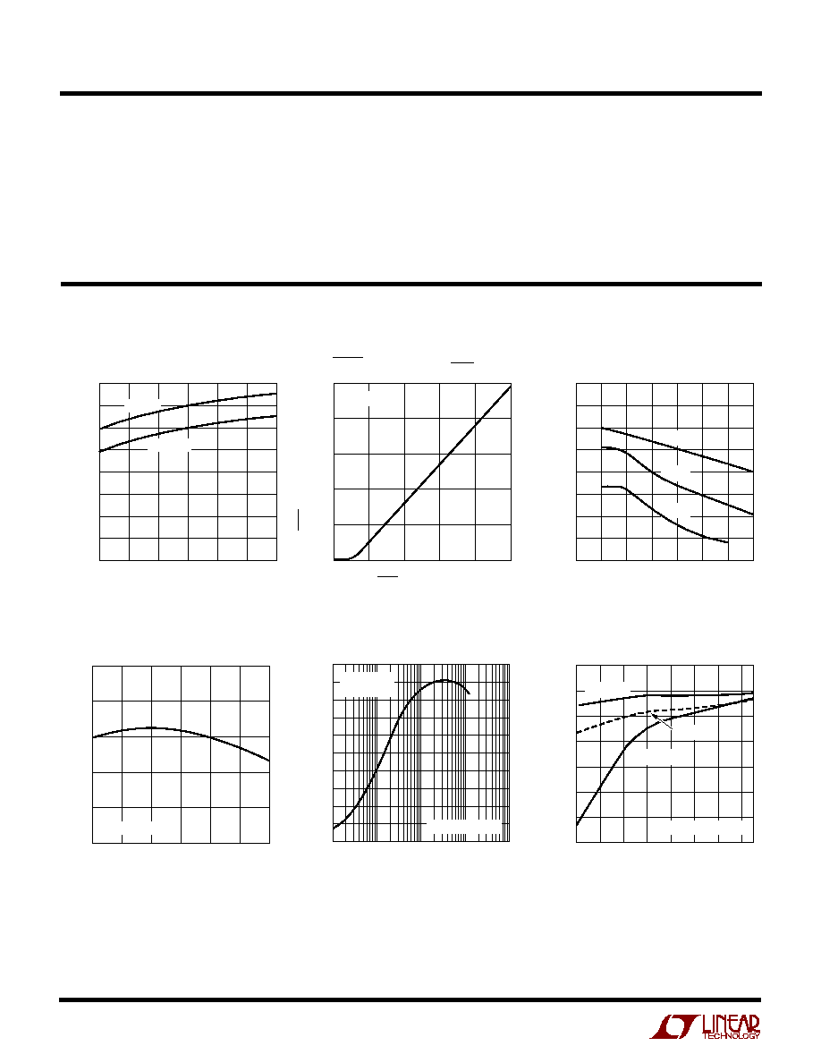
TYPICAL PERFOR A CE CHARACTERISTICS
U
W
Boost Converter Oscillator
Frequency vs Temperature
Boost Converter Current Limit
vs Duty Cycle
SHDN Pin Current vs V
SHDN
V
FB2
, Feedback Pin Voltage
TEMPERATURE (
°
C)
50
25
0
25
50
75
100
SWITCHING FREQUENCY (MHz)
3718 G01
2.00
1.75
1.50
1.25
1.00
0.75
0.50
0.25
0
V
IN
= 5V
V
IN
= 1.5V
SHDN PIN VOLTAGE (V)
0
1
2
3
4
5
SHDN PIN BIAS CURRENT (
µ
A)
3718 G02
50
40
30
20
10
0
T
A
= 25
°
C
DUTY CYCLE (%)
10
20
30
40
50
60
70
80
CURRENT LIMIT (mA)
3718 G03
1000
900
800
700
600
500
400
300
200
70
°
C
25
°
C
40
°
C
TEMPERATURE (
°
C)
50
FEEDBACK PIN VOLTAGE (V)
3718 G04
1.25
1.24
1.23
1.22
1.21
1.20
FIGURE 1 CIRCUIT
25
0
25
50
75
100
ELECTRICAL CHARACTERISTICS
Note 1: Absolute Maximum Ratings are those values beyond which the life
of a device may be impaired.
Note 2: T
J
is calculated from the ambient temperature T
A
and power
dissipation P
D
as follows:
LTC3718EG: T
J
= T
A
+ (P
D
· 130
°
C/W)
Note 3: The LTC3718 is tested in a feedback loop that adjusts V
FB1
to
achieve a specified error amplifier output voltage (I
TH
).
Note 4: The LTC3718 is guaranteed to meet performance specifications
from 0
°
C to 70
°
C. Specifications over the 40
°
C to 85
°
C operating
temperature range are assured by design, characterization and correlation
with statistical process controls.
Note 5: Current limit guaranteed by design and/or correlation to static test.
INPUT VOLTAGE (V)
1.5
1.7
1.9
2.1
2.3
2.5
2.7
2.9
V
OUT
/V
IN
(%)
3718 G06
50.00
49.95
49.90
49.85
49.80
49.75
49.70
49.65
LOAD = 0A
LOAD = 10A
FIGURE 1 CIRCUIT
LOAD = 1A
LOAD CURRENT (A)
EFFICIENCY (%)
100
90
80
70
60
50
40
30
20
10
0
0.01
1
10
100
3718 G05/TA01a
0.1
V
IN
= 2.5V
V
OUT
= 1.25V
FIGURE 1 CIRCUIT
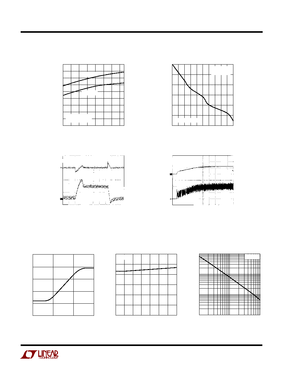
Efficiency vs Load Current
V
OUT
/V
IN
Tracking Ratio vs Input
Voltage
5
LTC3718
sn3718 3718fs
TYPICAL PERFOR A CE CHARACTERISTICS
U
W
1.5
1.7
1.9
2.1
2.3
2.5
2.7
2.9
INPUT VOLTAGE (V)
FREQUENCY (kHz)
3718 G07
450
400
350
300
250
200
150
100
50
0
LOAD = 0A
V
OUT
= 1.25V
FIGURE 1 CIRCUIT
LOAD = 10A
LOAD CURRENT (A)
0
1
2
3
4
5
6
7
8
9
10
V
OUT
/V
OUT
(%)
3718 G08
0
0.1
0.2
0.3
0.4
0.5
0.6
V
IN
= 2.5V
V
OUT
= 1.25V
FIGURE 1 CIRCUIT
Frequency vs Input Voltage
Load Regulation
Start-Up Response
V
IN
= 2.5V
4ms/DIV
3718 G09.eps
V
OUT
= 1.25V
LOAD = 0.2
FIGURE 1 CIRCUIT
V
OUT
1V/DIV
I
L
2A/DIV
Load-Step Transient
V
IN
= 2.5V
20
µ
s/DIV
3718 G10.eps
V
OUT
= 1.25V
LOAD = 500mA TO 10A STEP
FIGURE 1 CIRCUIT
V
OUT
200mV/DIV
I
L
5A/DIV
V
ON
VOLTAGE (V)
0
ON-TIME (ns) 400
600
3718 G11
200
0
1
2
3
1000
I
ION
= 30
µ
A
800
TEMPERATURE (
°
C)
50
ON-TIME (ns)
200
250
300
25
75
3718 G12
150
100
25
0
50
100
125
50
0
I
ION
= 30
µ
A
I
ON
CURRENT (
µ
A)
1
10
ON-TIME (ns)
100
1k
10k
10
100
3718 G13
V
VON
= 0V
On-Time vs V
ON
Voltage
On-Time vs
Temperature
On-Time vs I
ON
Current